US6513151B1 - Full flow focus exposure matrix analysis and electrical testing for new product mask evaluation - Google Patents
Full flow focus exposure matrix analysis and electrical testing for new product mask evaluation Download PDFInfo
- Publication number
- US6513151B1 US6513151B1 US09/794,503 US79450301A US6513151B1 US 6513151 B1 US6513151 B1 US 6513151B1 US 79450301 A US79450301 A US 79450301A US 6513151 B1 US6513151 B1 US 6513151B1
- Authority
- US
- United States
- Prior art keywords
- defect
- reticle
- wafer
- defects
- full flow
- Prior art date
- Legal status (The legal status is an assumption and is not a legal conclusion. Google has not performed a legal analysis and makes no representation as to the accuracy of the status listed.)
- Expired - Fee Related, expires
Links
Images


Classifications
-
- G—PHYSICS
- G03—PHOTOGRAPHY; CINEMATOGRAPHY; ANALOGOUS TECHNIQUES USING WAVES OTHER THAN OPTICAL WAVES; ELECTROGRAPHY; HOLOGRAPHY
- G03F—PHOTOMECHANICAL PRODUCTION OF TEXTURED OR PATTERNED SURFACES, e.g. FOR PRINTING, FOR PROCESSING OF SEMICONDUCTOR DEVICES; MATERIALS THEREFOR; ORIGINALS THEREFOR; APPARATUS SPECIALLY ADAPTED THEREFOR
- G03F7/00—Photomechanical, e.g. photolithographic, production of textured or patterned surfaces, e.g. printing surfaces; Materials therefor, e.g. comprising photoresists; Apparatus specially adapted therefor
- G03F7/70—Microphotolithographic exposure; Apparatus therefor
- G03F7/70483—Information management; Active and passive control; Testing; Wafer monitoring, e.g. pattern monitoring
- G03F7/7055—Exposure light control in all parts of the microlithographic apparatus, e.g. pulse length control or light interruption
- G03F7/70558—Dose control, i.e. achievement of a desired dose
-
- G—PHYSICS
- G03—PHOTOGRAPHY; CINEMATOGRAPHY; ANALOGOUS TECHNIQUES USING WAVES OTHER THAN OPTICAL WAVES; ELECTROGRAPHY; HOLOGRAPHY
- G03F—PHOTOMECHANICAL PRODUCTION OF TEXTURED OR PATTERNED SURFACES, e.g. FOR PRINTING, FOR PROCESSING OF SEMICONDUCTOR DEVICES; MATERIALS THEREFOR; ORIGINALS THEREFOR; APPARATUS SPECIALLY ADAPTED THEREFOR
- G03F7/00—Photomechanical, e.g. photolithographic, production of textured or patterned surfaces, e.g. printing surfaces; Materials therefor, e.g. comprising photoresists; Apparatus specially adapted therefor
- G03F7/70—Microphotolithographic exposure; Apparatus therefor
- G03F7/70483—Information management; Active and passive control; Testing; Wafer monitoring, e.g. pattern monitoring
- G03F7/70605—Workpiece metrology
- G03F7/70616—Monitoring the printed patterns
- G03F7/70625—Dimensions, e.g. line width, critical dimension [CD], profile, sidewall angle or edge roughness
-
- G—PHYSICS
- G03—PHOTOGRAPHY; CINEMATOGRAPHY; ANALOGOUS TECHNIQUES USING WAVES OTHER THAN OPTICAL WAVES; ELECTROGRAPHY; HOLOGRAPHY
- G03F—PHOTOMECHANICAL PRODUCTION OF TEXTURED OR PATTERNED SURFACES, e.g. FOR PRINTING, FOR PROCESSING OF SEMICONDUCTOR DEVICES; MATERIALS THEREFOR; ORIGINALS THEREFOR; APPARATUS SPECIALLY ADAPTED THEREFOR
- G03F7/00—Photomechanical, e.g. photolithographic, production of textured or patterned surfaces, e.g. printing surfaces; Materials therefor, e.g. comprising photoresists; Apparatus specially adapted therefor
- G03F7/70—Microphotolithographic exposure; Apparatus therefor
- G03F7/70483—Information management; Active and passive control; Testing; Wafer monitoring, e.g. pattern monitoring
- G03F7/70605—Workpiece metrology
- G03F7/70616—Monitoring the printed patterns
- G03F7/70641—Focus
-
- G—PHYSICS
- G03—PHOTOGRAPHY; CINEMATOGRAPHY; ANALOGOUS TECHNIQUES USING WAVES OTHER THAN OPTICAL WAVES; ELECTROGRAPHY; HOLOGRAPHY
- G03F—PHOTOMECHANICAL PRODUCTION OF TEXTURED OR PATTERNED SURFACES, e.g. FOR PRINTING, FOR PROCESSING OF SEMICONDUCTOR DEVICES; MATERIALS THEREFOR; ORIGINALS THEREFOR; APPARATUS SPECIALLY ADAPTED THEREFOR
- G03F7/00—Photomechanical, e.g. photolithographic, production of textured or patterned surfaces, e.g. printing surfaces; Materials therefor, e.g. comprising photoresists; Apparatus specially adapted therefor
- G03F7/70—Microphotolithographic exposure; Apparatus therefor
- G03F7/70483—Information management; Active and passive control; Testing; Wafer monitoring, e.g. pattern monitoring
- G03F7/70605—Workpiece metrology
- G03F7/70616—Monitoring the printed patterns
- G03F7/7065—Defects, e.g. optical inspection of patterned layer for defects
-
- G—PHYSICS
- G03—PHOTOGRAPHY; CINEMATOGRAPHY; ANALOGOUS TECHNIQUES USING WAVES OTHER THAN OPTICAL WAVES; ELECTROGRAPHY; HOLOGRAPHY
- G03F—PHOTOMECHANICAL PRODUCTION OF TEXTURED OR PATTERNED SURFACES, e.g. FOR PRINTING, FOR PROCESSING OF SEMICONDUCTOR DEVICES; MATERIALS THEREFOR; ORIGINALS THEREFOR; APPARATUS SPECIALLY ADAPTED THEREFOR
- G03F7/00—Photomechanical, e.g. photolithographic, production of textured or patterned surfaces, e.g. printing surfaces; Materials therefor, e.g. comprising photoresists; Apparatus specially adapted therefor
- G03F7/70—Microphotolithographic exposure; Apparatus therefor
- G03F7/70483—Information management; Active and passive control; Testing; Wafer monitoring, e.g. pattern monitoring
- G03F7/70605—Workpiece metrology
- G03F7/70653—Metrology techniques
- G03F7/70658—Electrical testing
Definitions
- the present invention generally relates to semiconductor processing, and in particular to a method and system for evaluating new product masks that includes detecting defects on a reticle containing the new product mask and evaluating the yield impact of such defects.
- lithography quality assurance engineers will run test wafers with focus exposure matrices to determine lithography process windows. Later in the wafer production process, development quality assurance personnel may run critical dimension (CD) splits at key layers to determine how variations are affecting the product performance. But each of these techniques suffer from drawbacks. For example, undersized contacts resulting from either repair, chrome defect or particle problems may not be detected, particularly when die-to-die comparisons are not available.
- CD critical dimension
- Analyzing a focus exposure matrix (FEM) on flat test wafers that have not been exposed to other topography influencing processes may not account for problems experienced due to such topography, and may similarly not account for interactions with non-lithography modules.
- examining a critical dimension (CD) split exposes but a part of the lithography process space, and may leave certain defects undetected.
- some reticle defects associated with new product masks may not be detected using these conventional methods.
- analyses concerning the effects, if any, on the production yield may not be performed, and thus manufacturing, repairing, and/or scrapping decisions may be made.
- a method for evaluating new products masks which includes detecting reticle defects and predicting the effect of such reticle defects on production yields of wafers printed using such a defective reticle is still required.
- the present invention provides for printing Focus Exposure Matrices (FEMs) on full flow production wafers as part of a hierarchy of Quality Assurance (QA) testing.
- FEMs can be formed from a plurality of patterns created with varying resist exposure dosages and stepper focuses. Thus, pattern shapes and/or line widths in the FEMs can vary within one wafer, which facilitates collecting data suitable for comparison analysis.
- Printing and analyzing such FEMs facilitates evaluating new product masks by facilitating detecting reticle defects and predicting product yields when a reticle with detected defects is employed to print wafers.
- the full flow production wafers (printed by the reticle containing the new product mask being evaluated), upon which the FEMs are printed at one or more different processing steps, are subjected, in addition, to end of line electrical testing, critical dimension measurement and analysis.
- the reticle is also subjected to a defect scan and a reticle scan that in turn lead to a printability simulation.
- reticle defects which may not be detected by conventional systems can be located, and analysis concerning the effects, if any, on production yield are facilitated.
- Lithography engineers employ reticle inspection tools to detect the existence of reticle defects. In the mask shop, reticle scans coupled with printability simulations can be employed to acquire first data. Then, in the Fab, engineers may employ automated defect inspection tools to review printed wafers, including wafers printed with FEMs, and to acquire more data associated with critical dimension measurements, for example. Finally, electrically testing FEM wafers can provide even more data that is suitable for defect identification and production yield analysis. To enable yield comparison, FEMs are printed on defective layers in full-flow production wafers, which facilitates comparisons with non-defective wafers. Such comparisons between empirically measured process windows and actual functional dies allows evaluation of the true process space when the lithography defect is combined with in-line process variation outside of the lithography module.
- the printability of reticle CD errors depends not only on the defect size, but also defect location, defect shape, and the proximity of the defect to other features.
- the effect of the defects may also be influenced by product specific sensitivity and interaction with non-lithographic modules.
- employing a method that incorporates data from analyses including analyzing FEMs on full flow production wafers facilitates improving new product mask evaluation and improving defect impact yield analysis.
- Analyzing FEMs printed on full flow production wafers in conjunction with reticle scans and printability simulation, flat wafer monitoring, critical dimension measurement and analysis facilitates collecting information in a plurality of ways. For reticles with more than one die per field, printing FEMs on actual full flow production wafers provides process sensitivity information at a functional level. As the position in the process window is varied across the wafer, dies can be compared to neighboring dies to scan for early yield roll off. At the bit level, the multi-tiered analysis approach facilitates identifying defect hot spots that may only occur under certain process conditions.
- a method for new product mask evaluation includes scanning a reticle and performing a printability simulation based, at least in part, on the reticle scanning.
- the method also includes performing defect scans on the printed wafers and flat wafer photo track monitoring.
- the method further includes performing critical dimension measuring and printing then analyzing one or more FEMs on full flow production wafers.
- the full flow production wafers are then subjected to end of line electrical testing to facilitate further defect detection, even at the bit level. Data gathered during the analysis phases of the method are then employed in performing a product yield analysis.
- Another aspect of the present invention provides a data packet adapted to be transmitted between two or more processes, the data packet containing defect analysis information and product yield information produced by a method for new product mask evaluation, where the method includes reticle scanning, printability simulating based, at least in part, on the reticle scanning, defect scanning, flat wafer photo track monitoring, critical dimension measuring, full flow product focus exposure matrix monitoring, end of line electrical testing, defect detection, and product yield analysis.
- the system includes a wafer defect analyzer, a reticle defect scanner operably coupled to the wafer defect analyzer, a printability simulator operably coupled to the wafer defect analyzer, a defect scanner operably coupled to the defect analyzer, a flat wafer monitor operably coupled to the defect analyzer, a critical dimension monitor operably coupled to the defect analyzer, a full flow product focus exposure matrix monitor operably coupled to the defect analyzer, and an end of line electrical tester operably coupled to the defect analyzer.
- a yield predictor is operably coupled to the system described above in this paragraph.
- FIG. 1 is a schematic diagram of a hierarchy of testing employed in accordance with an aspect of the present invention.
- FIG. 2 is a flow diagram illustrating one specific methodology for carrying out the present invention.
- FIG. 3 is a top view of a wafers imprinted with a focus exposure matrix, in accordance with an aspect of the present invention.
- FIG. 4 is a schematic block diagram illustrating a system for evaluating new product masks, the system detecting reticle defects, in accordance with an aspect of the present invention.
- FIG. 5 is a schematic block illustrating a system for evaluating new product masks, the system detecting reticle defects and producing yield estimates, in accordance with an aspect of the present invention.
- FIG. 6 is a schematic block diagram of an exemplary operating environment for a system configured in accordance with the present invention.
- FIG. 7 is a flow diagram illustrating one specific methodology for carrying out the present invention.
- FIG. 8 is a schematic block diagram illustrating a system for evaluating new product masks in accordance with an aspect of the present invention.
- component refers to a computer-related entity, either hardware, a combination of hardware and software, software, or software in execution.
- a component may be a process running on a processor, a processor, an object, an executable, a thread of execution, a program and a computer.
- an application running on a server and the server can be components.
- a component may reside in one physical location (e.g., in one computer) and/or may be distributed between two or more cooperating locations (e.g., parallel processing computer, computer network).
- non-linear training systems/methodologies e.g., back propagation, Bayesian, fuzzy sets, non-linear regression, or other neural networking paradigms including mixture of experts, cerebella model arithmetic computer (CMACS), radial basis functions, directed search networks and function link networks may be employed.
- CMACS cerebella model arithmetic computer
- a hierarchy 100 of testing employed in evaluating a new product mask is evaluated.
- actions associated with analyzing a reticle containing the new product mask can include, but are not limited to, scanning the reticle and performing printability simulations.
- actions associated with analyzing a production wafer and/or test wafers as they are being processed where such processing includes patterning the wafer by employing the reticle containing the new product mask.
- flat wafer monitoring including analyzing one or more focus exposure matrices on the flat wafer, can occur.
- analyzing one or more focus exposure matrices on a full flow product wafer can occur. Performing analyses on both test wafers and full flow production wafers facilitates collecting comparative data that in turn facilitates evaluating reticle defects in the context in a product and feature sensitive manner. Further, printing and then analyzing one or more focus exposure matrices on a full flow product wafer facilitates collecting data associated with defects that may only become apparent under actual production run conditions.
- analyses performed on substantially completed wafers is undertaken. For example, analysis including, but not limited to, electrical analysis of circuits on the wafer can be undertaken.
- data that can be employed to detect reticle defects and to determine the effect on production yields can be collected from several processes in the processing cycle, which facilitates producing improvements in new product mask evaluation by improving reticle defect detection and product yield analysis, as compared to conventional systems.
- FIG. 2 is a flow diagram illustrating one particular methodology 200 for carrying out the present invention.
- general initializations are performed. Such initializations can include, but are not limited to, allocating memory, establishing pointers, establishing data communications, initializing variables, initializing data structures and instantiating objects.
- action is taken on a reticle containing a new product mask.
- the reticle containing the new product mask is scanned. Such reticle scanning may be performed by devices including, but not limited to a KLA-Tencor STARlightTM system that employs simultaneous transmitted and reflected-light contamination inspection.
- printability simulation is performed.
- Printability simulation involves off-line methods for predicting how features and defects in reticles will print on full flow production wafers.
- Light transmitted through a reticle can be processed by a photolithography simulator, which can produce predicted aerial images.
- Predicted critical dimensions can be calculated from the simulation and compared to data collected from later processes that measure actual critical dimensions. Such comparisons facilitate producing yield estimates.
- blocks 235 through 270 actions are performed on wafers as they are being produced. It will be understood by one skilled in the art that blocks 235 through 270 may be performed one or more times during one or more processing phases of a wafer.
- an integrated circuit being fabricated on a wafer may include a plurality of layers. Blocks 235 through 270 may be performed for one or more of the plurality of layers.
- one or more FEMs are processed onto a wafer. While one block 235 is illustrated, it is to be appreciated that one or more FEMs may be developed on one or more layers of an integrated circuit to be fabricated on a wafer.
- a wafer and/or a pattern on a wafer exposed through the reticle containing the new product mask are scanned for defects.
- defect scanning can be performed by devices including, but not limited to, a KLA2132 processor, for example.
- the defect scanning of block 240 can produce data that can be correlated with data acquired during the reticle scan of block 220 .
- data not retrieved by conventional systems, which do not print FEMs on full flow production wafers may be acquired during the scan at 240 .
- Such data may incorporate data that can only be acquired from full flow production wafers (e.g., topography dependent data, production run stepper and/or spin track conditions).
- the KLA2132 wafer defect inspection tools may similarly be employed in flat wafer monitoring at block 250 .
- Such flat wafer monitoring may include image qualification.
- Image qualification involves applying a patterned photoresist to a flat silicon wafer and then performing automated die-to-die defect inspection.
- the KLA2132 inspection tools can be run at different levels than those employed for analyzing full flow product wafers, which facilitates acquiring different data that facilitates detecting more defects than conventional systems.
- Photo Track Monitoring (PTM), or Photo Cell Monitoring (PCM) can be employed in such lithographic defect monitoring. It is to be appreciated, that flat wafers may be monitored at one or more of the processing phases through which an integrated circuit will pass during fabrication.
- a repeating defect is a defect that appears in multiple wafers at the same location.
- the repeating defect can be an indicator that a reticle has a defect, as opposed to the defect being caused by a one-time contamination problem or wafer-to-wafer variations.
- critical dimensions of features formed in one or more layers on the integrated circuit being fabricated on the wafer, where such fabrication employs the reticle containing the new product mask being evaluated, can be measured. Such critical dimensions may be compared to predicted critical dimensions, where such predictions were made during block 230 . Measuring critical dimensions is well known in the art and thus, for the sake of brevity is not discussed herein.
- FEMs Focus Exposure Matrices
- FEMs can be printed on layers including, but not limited to, gate oxide layers, field oxide layers and contact layers, for example. Analysis can be performed for FEMs located upon each layer wherein the FEMs are printed.
- FEMs By printing FEMs on full flow production wafers, with production topography produced by production processing, rather than solely on test and/or flat wafers, data points not conventionally retrieved may be acquired. Such data can facilitate detecting defects not detected by conventional systems. Furthermore, such data is suitable for comparison to printability simulation data to facilitate predicting production yields.
- data retrieved from such context sensitive processing can be employed to detect reticle defects that may only appear on production wafers, and that would not appear on flat “test” wafers.
- end of line electrical testing can be performed upon full flow production wafers upon which FEMs have been printed and/or analyzed.
- the end of line electrical testing of block 280 can include, but is not limited to, bit level failure analysis that facilitates aggregating bit level data across multiple non-functional dies. Correlating data between multiple dies facilitates identifying reticle defects that may go undetected by conventional systems.
- reticle defect detection based on data collected during the preceding steps may occur.
- correlating potential reticle detect defect data gathered during block 220 with wafer defect coordinate data gathered at block 280 may facilitate identifying reticle defects that maybe undetected if no such correlation were performed. Employing such correlations provides yet another improvement over conventional systems. It is to be understood that while coordinate correlation is provided as one example of data processing that can be employed in defect detection at block 290 , that other correlations of data collected at different blocks may be employed in accordance with the present invention. For example, defect scan data collected at block 240 while may be correlated with bit level error data collected at block 280 . Similarly, FEM related data and analysis collected and/or performed at block 270 may be correlated with data from the end of line electric testing of block 280 .
- a yield analysis is performed. It is to be appreciated that in other examples of the present invention, the yield analysis of block 292 may be omitted.
- Reticle defect detection data can be processed in association with printability simulation data and actual wafer defect detection data to produce predictions concerning anticipated yields when wafers are processed using the new product mask incorporated into the reticle evaluated in blocks 210 through 290 .
- a first detected defect in the new product mask may be predicted to lead to a ten percent reduction in yield, due to the location of the defect and the relationship of the defect to surrounding features while a second detected defect may be predicted to lead to a forty percent reduction in yield due to a different size, shape and/or location of the defect.
- Data gathered from FEMs printed on full flow production wafers, and analysis associated with such data facilitates generating a confidence level in the predictions of block 292 , thus facilitating decisions concerning whether to use the reticle with the new product mask, to discard the reticle, or to attempt repairs of the reticle, which provides improvements over conventional systems.
- FIG. 3 is a top view of a flat test wafer 300 with a focus exposure matrix 310 imprinted thereon.
- FIG. 3 also includes a top view of a full flow production wafer 320 with a focus exposure matrix 330 imprinted thereon and a wafer 340 with a focus exposure matrix 350 printed thereon.
- Printing and analyzing one or more FEMs 310 on a test wafer 300 facilitates collecting certain types of data while printing and analyzing one or more FEMs 330 on a full flow production wafer 320 facilitates collecting other types of data.
- image qualification involves applying a patterned photoresist to a flat silicon wafer and then performing automated die-to-die defect inspection.
- inspection tools can be run at levels that cannot be employed with full flow production wafers 320 , which facilitates detecting defects.
- analyzing FEMs 330 on full flow production wafers 320 provides data that cannot be gathered from test wafers 300 that have not undergone the same processing steps as the full flow production wafer 320 and which do not have the topography resulting from lithography processes (e.g., deposition, development, etching) on the full flow production wafer 320 .
- lithography processes e.g., deposition, development, etching
- FIG. 3 also illustrates a wafer 340 upon which an FEM 350 is printed.
- the FEM 350 is illustrated as a series of intersecting lines.
- the FEM 310 and the FEM 330 are illustrated as a series of parallel lines. It is to be appreciated that the FEMs 310 , 330 and 350 are merely illustrative, and that an FEM may be formed from one or more lines, circles and/or other geometric shapes. FEMs can also be formed from a plurality of patterns created with varying resist exposure dosages and stepper focuses. Thus, the pattern shapes and/or line widths can vary within one wafer, which facilitates collecting data suitable for comparison analysis.
- FIG. 4 is a schematic block diagram illustrating a system 400 for evaluating a new product mask, where the system detects reticle defects.
- the system 400 includes a defect analyzer 410 that can receive analysis data from one or more reticle and/or wafer analyzing components and perform analyses that produce information concerning defects in new product masks.
- the system 400 includes a reticle scanner 430 .
- the reticle scanner 430 may be, for example, a KLA-Tencor STARlightTM system that employs simultaneous transmitted and reflected-light contamination inspection.
- the reticle scanner 430 can produce data that is sent to the defect analyzer 410 .
- Such data may include, but is not limited to, defects detected, defects suspected, and coordinates of such detected and/or suspected defects.
- the system 400 includes a printability simulator 440 adapted to produce images simulating one or more patterns on a wafer printed with the reticle scanned by the reticle scanner 430 . Data from the reticle scanner can be forwarded to the defect analyzer 410 . Images produced by the printability Simulator 440 facilitate detecting defects in the new product mask on the reticle that may produce defects in the pattern exposed on the wafer. But the printability simulator 440 may not detect all the defects in a reticle. Thus, the system 400 includes a defect scanner 450 that can be employed to scan a pattern exposed into a layer on a wafer for defects.
- Data from the defect scanner 450 is forwarded to the defect analyzer 410 , and can be correlated with data from the printability simulator 440 , for example, to facilitate evaluating the operation of the defect scanner 450 and the reticle scanner 430 .
- the reticle scanner 430 determines that a defect exists at a certain location in the new product mask contained on the reticle scanned by the reticle scanner 430
- data collected by the defect scanner 450 can be employed to confirm that the reticle defect produces a print defect. Such confirmation may also be employed in evaluating the performance of the printability simulator 440 .
- Data generated by the defect scanner 450 can similarly be forwarded to the defect analyzer 410 .
- the system 400 includes a flat wafer monitor 460 .
- the flat wafer monitor 460 can be employed to collect data from test wafers that may not contain topographical features present in full flow product wafers.
- the flat wafer monitor may be, for example, a KLA2132 wafer defect inspection tool.
- the flat wafers may have one or more FEMs printed thereon.
- the FEMs printed on the flat wafers may be related to the FEMs printed on full flow product wafers, which facilitates comparing and contrasting data retrieved by analyzing such FEMs, with such comparison analysis facilitating isolating defects associated with topography and full flow production conditions (e.g., stepper parameters, spin track parameters).
- Data generated by the flat wafer monitor 460 can similarly be forwarded to the defect analyzer 410 .
- the system 400 includes a critical dimension (CD) monitor 470 .
- CD monitors are well known in the art, and thus, for the sake of brevity, are not discussed herein.
- Data generated by the critical dimension monitor 470 can similarly be forwarded to the defect analyzer 410 , to facilitate detecting defects in new product masks.
- the system 400 includes a full flow product wafer FEM monitor 480 .
- An FEM is formed from a plurality of patterns created with varying resist exposure dosages and stepper focuses. Thus, pattern shapes and/or line widths in the FEMs can vary within one wafer, which facilitates collecting data suitable for comparison analysis.
- Printing and analyzing such FEMs facilitates evaluating new product masks by facilitating detecting reticle defects and predicting product yields when a reticle with detected defects is employed to print wafers.
- Printing and then analyzing FEMs on full flow product wafers further facilitates collecting defect data related to topography and production process parameters (e.g., stepper parameters, spin track parameters). Data generated by the FEM monitor 480 can similarly be forwarded to the defect analyzer 410 .
- the system 400 includes an end of line electrical tester 490 .
- the end of line electrical tester 490 can be employed to generate, for example, bit level failure analysis that facilitates aggregating bit level data across multiple non-functional dies. Correlating data between multiple dies facilitates identifying reticle defects that may go undetected by conventional systems. Data generated by the end of line electrical tester 490 can similarly be forwarded to the defect analyzer 410 .
- the defect analyzer 410 thus has data available from a plurality of sources, including the FEM monitor 480 , which facilitates evaluating a new product mask, facilitating improvements over conventional systems.
- FIG. 5 is a schematic block illustrating a system 500 for evaluating a new product mask, where the system detects reticle defects and produces yield estimates.
- the system 500 includes a defect analyzer 510 that can receive analysis data from one or more reticle and/or wafer analyzing components.
- the system 500 includes a yield predictor 520 operably connected to the defect analyzer 510 .
- the yield predictor 520 is adapted to output data concerning yields that can be expected if wafers are processed using a new product mask evaluated by the defect analyzer 510 .
- a first defect detected in the new product mask may be predicted to lead to a ten percent reduction in yield, due to the location of the defect and the relationship of the defect to surrounding features.
- a confidence level associated with the prediction can be achieved by comparing the predicted yield with actual yields from full production wafers analyzed by the present invention.
- a second detected defect may be predicted to lead to a forty percent reduction in yield due to a different size, shape and/or location of the defect, and data collected from FEMs analyzed on full flow production wafers and/or flat wafers. With such predictions, and such confidence levels in such predictions, decisions concerning fabricating integrated circuits by employing the new product mask are facilitated.
- the new product mask may be discarded, and a new supplier of product masks may be sought.
- the system 500 includes a reticle scanner 530 that produces data that is sent to the defect analyzer 510 .
- data may include, but is not limited to, defects detected, defects suspected, and coordinates of such detected and/or suspected defects.
- the system 500 includes a printability simulator 540 adapted to produce images simulating one or more patterns on a wafer printed with the new product mask on the reticle scanned by the reticle scanner 530 . Data from the reticle scanner can be forwarded to the defect analyzer 510 . Images produced by the printability simulator 540 facilitate detecting defects in the new product mask on the reticle that may produce defects in the pattern exposed on the wafer. But the printability simulator 540 may not detect all the defects in a reticle. Thus, the system 500 includes a defect scanner 550 that can be employed to scan a pattern exposed into a layer on a wafer for defects.
- Data from the defect scanner 550 is forwarded to the defect analyzer 510 , and can be correlated with data from the printability simulator 540 , for example, to facilitate evaluating the operation of the defect scanner 550 and the reticle scanner 530 .
- Data generated by the defect scanner 550 can similarly be forwarded to the defect analyzer 510 .
- the system 500 includes a flat wafer monitor 560 .
- the flat wafer monitor 560 can be employed to collect data from test wafers that may not contain topographical features present in full flow product wafers.
- the flat wafers may have one or more FEMs printed thereon.
- the FEMs printed on the flat wafers may be related to the FEMs printed on full flow product wafers, which facilitates comparing and contrasting data retrieved by analyzing such FEMs, with such comparison analysis facilitating isolating defects associated with topography and full flow production conditions (e.g., stepper parameters, spin track parameters).
- Data generated by the flat wafer monitor 560 can similarly be forwarded to the defect analyzer 510 .
- the system 500 includes a critical dimension monitor 570 .
- Such critical dimension monitors are well known in the art, and thus, for the sake of brevity, are not discussed herein. Data generated by the critical dimension monitor 570 can similarly be forwarded to the defect analyzer 510 .
- the system 500 includes a full flow product wafer FEM monitor 580 . Data generated by the FEM monitor 580 can similarly be forwarded to the defect analyzer 510 to facilitate evaluating new product masks.
- the system 500 includes an end of line electrical tester 590 .
- the end of line electrical tester 590 can be employed to generate, for example, bit level failure analysis that facilitates aggregating bit level data across multiple non-functional dies. Correlating data between multiple dies facilitates identifying reticle defects that may go undetected by conventional systems. Data generated by the end of line electrical tester 590 can similarly be forwarded to the defect analyzer 510 where it can be employed to facilitate evaluating new product masks.
- the defect analyzer 510 thus has data available from a plurality of sources, including the FEM monitor 580 , which facilitates evaluating a new product mask, facilitating improvements over conventional systems.
- the data collected from the plurality of sources an then be made available to the yield predictor 520 , which can lead to improvements in integrated circuit manufacturing efficiency.
- FIG. 6 is a schematic block diagram of an exemplary operating environment for a system configured in accordance with the present invention.
- FIG. 6 and the following discussion are intended to provide a brief, general description of a suitable computing environment 610 in which the various aspects of the present invention may be implemented. While the invention has been described above in the general context of computer-executable instructions that may run on one or more computers, those skilled in the art will recognize that the invention also may be implemented in combination with other program modules and/or as a combination of hardware and software.
- program modules include routines, programs, components, data structures, etc. that perform particular tasks or implement particular abstract data types.
- inventive methods may be practiced with other computer system configurations, including single-processor or multiprocessor computer systems, minicomputers, mainframe computers, as well as personal computers, hand-held computing devices, microprocessor-based or programmable consumer electronics, and the like, each of which may be operatively coupled to one or more associated devices.
- inventive methods may also be practiced in distributed computing environments where certain tasks are performed by remote processing devices that are linked through a communications network.
- program modules may be located in both local and remote memory storage devices.
- an exemplary environment 610 for implementing various aspects of the invention includes a computer 612 , the computer 612 including a processing unit 614 , a system memory 616 and a system bus 618 .
- the system bus 618 couples system components including, but not limited to, the system memory 616 to the processing unit 614 .
- the processing unit 614 may be any of various commercially available processors. Dual microprocessors and other multi-processor architectures also can be employed as the processing unit 614 .
- the system bus 618 can be any of several types of bus structure including a memory bus or memory controller, a peripheral bus and a local bus using any of a variety of commercially available bus architectures.
- the system memory 622 includes read only memory (ROM) 620 and random access memory (RAM) 622 .
- ROM read only memory
- RAM random access memory
- the computer 612 further includes a hard disk drive 624 , a magnetic disk drive 626 , (e.g., to read from or write to a removable disk 628 ) and an optical disk drive 630 , (e.g., for reading a CD-ROM disk 632 or to read from or write to other optical media).
- the hard disk drive 624 , magnetic disk drive 626 and optical disk drive 630 can be connected to the system bus 618 by a hard disk drive interface 634 , a magnetic disk drive interface 636 and an optical drive interface 638 , respectively.
- the drives and their associated computer-readable media provide nonvolatile storage of data, data structures, computer-executable instructions, etc. for the computer 612 , including for the storage of broadcast programming in a suitable digital format.
- computer-readable media refers to a hard disk, a removable magnetic disk and a CD
- other types of media which are readable by a computer such as zip drives, magnetic cassettes, flash memory cards, digital video disks, cartridges, and the like, may also be used in the exemplary operating environment, and further that any such media may contain computer-executable instructions for performing the methods of the present invention.
- a number of program modules can be stored in the drives and RAM 622 , including an operating system 640 , one or more application programs 642 , other program modules 644 and program data 646 . It is to be appreciated that the present invention can be implemented with various commercially available operating systems or combinations of operating systems.
- a user can enter commands and information into the computer 612 through a keyboard 648 and a pointing device, such as a mouse 650 .
- Other input devices may include a microphone, an IR remote control, a joystick, a game pad, a satellite dish, cameras, in the sense of gesture interpreted through cameras and machine-vision software, a scanner, or the like.
- These and other input devices are often connected to the processing unit 614 through a serial port interface 652 that is coupled to the system bus 618 , but may be connected by other interfaces, such as a parallel port, a game port, a universal serial bus (“USB”), an IR interface, etc.
- a monitor 654 or other type of display device is also connected to the system bus 618 via an interface, such as a video adapter 656 .
- a computer typically includes other peripheral output devices (not shown), such as speakers, printers etc.
- the computer 612 may operate in a networked environment using logical connections to one or more remote computers, such as a remote computer(s) 658 .
- the remote computer(s) 658 may be a workstation, a server computer, a router, a personal computer, microprocessor based entertainment appliance, a peer device or other common network node, and typically includes many or all of the elements described relative to the computer 612 , although, for purposes of brevity, only a memory storage device 660 is illustrated.
- the logical connections depicted include a local area network (LAN) 662 and a wide area network (WAN) 664 .
- LAN local area network
- WAN wide area network
- the computer 612 When used in a LAN networking environment, the computer 612 is connected to the local network 662 through a network interface or adapter 666 .
- the computer 612 When used in a WAN networking environment, the computer 612 typically includes a modem 668 , or is connected to a communications server on the LAN, or has other means for establishing communications over the WAN 664 , such as the Internet.
- the modem 668 which may be internal or external, is connected to the system bus 618 via the serial port interface 652 .
- program modules depicted relative to the computer 612 may be stored in the remote memory storage device 660 . It will be appreciated that the network connections shown are exemplary and other means of establishing a communications link between the computers may be used.
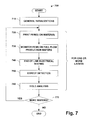
- FIG. 7 a flow diagram illustrates one particular methodology 700 for carrying out the present invention.
- the methodology 700 involves combining FEM analysis with end of line electrical testing to facilitate new product mask evaluation.
- initializations are performed. Such initializations can include, but are not limited to, allocating memory, establishing pointers, establishing data communications, initializing variables, initializing data structures and instantiating objects.
- one or more FEMs are printed on a full flow product wafer.
- the FEMs can be formed from a plurality of patterns created with varying resist exposure dosages and stepper focuses.
- the FEMs may be formed from one or more lines, circles and/or other geometric shapes.
- the FEMs of block 720 are monitored for parameters including, but not limited to, size, shape, location, degree to which lines are parallel, degree to which lines are perpendicular, line length, line width and line area. Monitoring the FEMs for such parameters facilitates detecting printing defects due to defects in a new product mask.
- the wafer upon which the FEMs have been processed can be subjected to electrical testing.
- electrical testing integrated circuits manufactured, at least in part, in association with the new product mask being evaluated, are analyzed to determine whether desired electrical operation of the integrated circuit occurs or whether undesired operation occurs. The presence and/or absence of such undesired operation can be correlated with analysis performed on the FEMs to provide improved evaluation of new product masks as compared to conventional systems.
- the defect detection of 750 can be followed at 760 by a yield analysis.
- a yield analysis may be undertaken to predict estimated yields of operable integrated circuits manufactured using the new product mask being evaluated.
- a determination is made concerning whether more wafers remain to be analyzed. If the determination at 770 is NO, then processing concludes, otherwise, if the determination at 770 is YES, then processing can return to 720 .
- the system 800 includes a defect analyzer 810 that receives input from an FEM printer 830 , a full flow product wafer FEM monitor 840 and an end-of-line electrical tester 850 .
- the defect analyzer accepts such inputs, and produces an output concerning defects detected with a new product mask being analyzed.
- the FEM printer 830 prints one or more FEMs on full flow product wafers.
- the FEMs can be formed from a plurality of patterns created with varying resist exposure dosages and stepper focuses.
- the FEMs may be formed from one or more lines, circles and/or other geometric shapes.
- the FEMs are processed so as to not interfere with the electrical operation of the one or more integrated circuits being fabricated on the wafer on which the FEMs are processed.
- the full flow product wafer FEM monitor 840 can monitor one or more FEMs for parameters including, but not limited to, size, shape, location, degree to which lines are parallel, degree to which lines are perpendicular, line length, line width and line area. Monitoring the FEMs for such parameters facilitates detecting printing defects due to defects in a new product mask, and thus leads to improved quality control in integrated circuit manufacture.
- the end of line electrical tester 850 can test integrated circuits exposed to the new product mask being evaluated, to determine whether desired electrical operation of the integrated circuit occurs or whether undesired operation occurs. The presence and/or absence of such undesired operation can be correlated with analysis performed on the FEMs to provide improved evaluation of new product masks as compared to conventional systems, which in turn leads to improved integrated circuit quality assurance.
- the defect analyzer 810 can pass through data collected from the FEM printer 830 , the full flow product wafer FEM monitor 840 and the end-of-line electrical tester 850 and/or data derived from such data, to a yield predictor 820 .
- the yield predictor 820 can then be employed to determine estimated yields of integrated circuits fabricated using the new product mask being evaluated.
- decisions concerning the disposition of a new product mask e.g., employ, repair, destroy
- integrated circuit manufacture can benefit from increased efficiency.
Abstract
Description
Claims (27)
Priority Applications (1)
| Application Number | Priority Date | Filing Date | Title |
|---|---|---|---|
| US09/794,503 US6513151B1 (en) | 2000-09-14 | 2001-02-26 | Full flow focus exposure matrix analysis and electrical testing for new product mask evaluation |
Applications Claiming Priority (2)
| Application Number | Priority Date | Filing Date | Title |
|---|---|---|---|
| US23297600P | 2000-09-14 | 2000-09-14 | |
| US09/794,503 US6513151B1 (en) | 2000-09-14 | 2001-02-26 | Full flow focus exposure matrix analysis and electrical testing for new product mask evaluation |
Publications (1)
| Publication Number | Publication Date |
|---|---|
| US6513151B1 true US6513151B1 (en) | 2003-01-28 |
Family
ID=26926518
Family Applications (1)
| Application Number | Title | Priority Date | Filing Date |
|---|---|---|---|
| US09/794,503 Expired - Fee Related US6513151B1 (en) | 2000-09-14 | 2001-02-26 | Full flow focus exposure matrix analysis and electrical testing for new product mask evaluation |
Country Status (1)
| Country | Link |
|---|---|
| US (1) | US6513151B1 (en) |
Cited By (55)
| Publication number | Priority date | Publication date | Assignee | Title |
|---|---|---|---|---|
| US20030048458A1 (en) * | 2001-06-26 | 2003-03-13 | Walter Mieher | Method for determining lithographic focus and exposure |
| US6617087B1 (en) * | 2001-06-27 | 2003-09-09 | Advanced Micro Devices, Inc. | Use of scatterometry to measure pattern accuracy |
| US20030212518A1 (en) * | 2002-05-09 | 2003-11-13 | Johnson & Johnson | System and method for quality performance evaluation and reporting |
| US20040015808A1 (en) * | 1997-09-17 | 2004-01-22 | Numerical Technologies, Inc. | System and method for providing defect printability analysis of photolithographic masks with job-based automation |
| US20040181728A1 (en) * | 2003-03-11 | 2004-09-16 | Joseph Pellegrini | Methods and systems for estimating reticle bias states |
| US20040190008A1 (en) * | 2003-01-17 | 2004-09-30 | Kla-Tencor Corporation | Method for process optimization and control by comparison between 2 or more measured scatterometry signals |
| US20050004774A1 (en) * | 2003-07-03 | 2005-01-06 | William Volk | Methods and systems for inspection of wafers and reticles using designer intent data |
| US6845345B1 (en) * | 2001-02-06 | 2005-01-18 | Advanced Micro Devices, Inc. | System for monitoring and analyzing diagnostic data of spin tracks |
| WO2005069191A1 (en) * | 2003-12-31 | 2005-07-28 | Pdf Solutions, Inc. | Method and system for failure signal detection analysis |
| US20050204328A1 (en) * | 2004-03-12 | 2005-09-15 | Strelkova Nadya G. | Method for verifying ret latent image sensitivity to mask manufacturing errors |
| US20060022693A1 (en) * | 2004-07-27 | 2006-02-02 | International Business Machines Corporation | Circuit and method for monitoring defects |
| US20060062445A1 (en) * | 2004-09-14 | 2006-03-23 | Gaurav Verma | Methods, systems, and carrier media for evaluating reticle layout data |
| US20060150841A1 (en) * | 2005-01-07 | 2006-07-13 | Heidelberger Druckmaschinen Ag | Printing press |
| US7079975B1 (en) * | 2001-04-30 | 2006-07-18 | Advanced Micro Devices, Inc. | Scatterometry and acoustic based active control of thin film deposition process |
| US20060161452A1 (en) * | 2004-01-29 | 2006-07-20 | Kla-Tencor Technologies Corp. | Computer-implemented methods, processors, and systems for creating a wafer fabrication process |
| US20060242619A1 (en) * | 1997-09-17 | 2006-10-26 | Synopsys, Inc. | System And Method For Providing Defect Printability Analysis Of Photolithographic Masks With Job-Based Automation |
| US20060265221A1 (en) * | 2005-05-20 | 2006-11-23 | Dictaphone Corporation | System and method for multi level transcript quality checking |
| US20060291714A1 (en) * | 2004-12-07 | 2006-12-28 | Kenong Wu | Computer-implemented methods for detecting and/or sorting defects in a design pattern of a reticle |
| US20070156379A1 (en) * | 2005-11-18 | 2007-07-05 | Ashok Kulkarni | Methods and systems for utilizing design data in combination with inspection data |
| US20070230770A1 (en) * | 2005-11-18 | 2007-10-04 | Ashok Kulkarni | Methods and systems for determining a position of inspection data in design data space |
| US20070288219A1 (en) * | 2005-11-18 | 2007-12-13 | Khurram Zafar | Methods and systems for utilizing design data in combination with inspection data |
| US20080072207A1 (en) * | 2006-06-29 | 2008-03-20 | Gaurav Verma | Computer-implemented methods and systems for determining different process windows for a wafer printing process for different reticle designs |
| US7379175B1 (en) * | 2002-10-15 | 2008-05-27 | Kla-Tencor Technologies Corp. | Methods and systems for reticle inspection and defect review using aerial imaging |
| US20080167829A1 (en) * | 2007-01-05 | 2008-07-10 | Allen Park | Methods and systems for using electrical information for a device being fabricated on a wafer to perform one or more defect-related functions |
| US20090016595A1 (en) * | 2007-05-09 | 2009-01-15 | Peterson Ingrid B | Methods and systems for detecting defects in a reticle design pattern |
| US20090024967A1 (en) * | 2007-05-07 | 2009-01-22 | Bo Su | Computer-implemented methods, systems, and computer-readable media for determining a model for predicting printability of reticle features on a wafer |
| US20090043527A1 (en) * | 2007-08-10 | 2009-02-12 | Allen Park | Computer-implemented methods, carrier media, and systems for generating a metrology sampling plan |
| US20090041332A1 (en) * | 2007-07-20 | 2009-02-12 | Kla-Tencor Corporation | Methods for generating a standard reference die for use in a die to standard reference die inspection and methods for inspecting a wafer |
| US20090055783A1 (en) * | 2007-08-20 | 2009-02-26 | Kla-Tencor Corporation | Computer-implemented methods for determining if actual defects are potentially systematic defects or potentially random defects |
| US20090235212A1 (en) * | 2008-03-12 | 2009-09-17 | Daubenspeck Timothy H | Design structure, failure analysis tool and method of determining white bump location using failure analysis tool |
| US20090257645A1 (en) * | 2008-04-14 | 2009-10-15 | Chen Chien-Huei Adam | Methods and systems for determining a defect criticality index for defects on wafers |
| US20100011325A1 (en) * | 2008-07-08 | 2010-01-14 | Synopsys, Inc. | Method and apparatus for determining the effect of process variations |
| US7738093B2 (en) | 2007-05-07 | 2010-06-15 | Kla-Tencor Corp. | Methods for detecting and classifying defects on a reticle |
| US7769225B2 (en) | 2005-08-02 | 2010-08-03 | Kla-Tencor Technologies Corp. | Methods and systems for detecting defects in a reticle design pattern |
| US20100235134A1 (en) * | 2009-03-13 | 2010-09-16 | Kla-Tencor Corporation | Methods and systems for generating an inspection process for a wafer |
| US7877722B2 (en) | 2006-12-19 | 2011-01-25 | Kla-Tencor Corp. | Systems and methods for creating inspection recipes |
| CN101546112B (en) * | 2008-03-25 | 2011-04-20 | 中芯国际集成电路制造(上海)有限公司 | Method for replacing mask |
| US20120005634A1 (en) * | 2010-06-30 | 2012-01-05 | Globalfoundries Inc. | Control of Critical Dimensions in Optical Imaging Processes for Semiconductor Production by Extracting Imaging Imperfections on the Basis of Imaging Tool Specific Intensity Measurements and Simulations |
| US8204297B1 (en) | 2009-02-27 | 2012-06-19 | Kla-Tencor Corp. | Methods and systems for classifying defects detected on a reticle |
| US8407632B2 (en) | 2010-09-14 | 2013-03-26 | International Business Machines Corporation | Detecting dose and focus variations during photolithography |
| US8775101B2 (en) | 2009-02-13 | 2014-07-08 | Kla-Tencor Corp. | Detecting defects on a wafer |
| US8781781B2 (en) | 2010-07-30 | 2014-07-15 | Kla-Tencor Corp. | Dynamic care areas |
| US8826200B2 (en) | 2012-05-25 | 2014-09-02 | Kla-Tencor Corp. | Alteration for wafer inspection |
| US8831334B2 (en) | 2012-01-20 | 2014-09-09 | Kla-Tencor Corp. | Segmentation for wafer inspection |
| US9053527B2 (en) | 2013-01-02 | 2015-06-09 | Kla-Tencor Corp. | Detecting defects on a wafer |
| US9087367B2 (en) | 2011-09-13 | 2015-07-21 | Kla-Tencor Corp. | Determining design coordinates for wafer defects |
| US9092846B2 (en) | 2013-02-01 | 2015-07-28 | Kla-Tencor Corp. | Detecting defects on a wafer using defect-specific and multi-channel information |
| US9134254B2 (en) | 2013-01-07 | 2015-09-15 | Kla-Tencor Corp. | Determining a position of inspection system output in design data space |
| US9170211B2 (en) | 2011-03-25 | 2015-10-27 | Kla-Tencor Corp. | Design-based inspection using repeating structures |
| US9189844B2 (en) | 2012-10-15 | 2015-11-17 | Kla-Tencor Corp. | Detecting defects on a wafer using defect-specific information |
| US9311698B2 (en) | 2013-01-09 | 2016-04-12 | Kla-Tencor Corp. | Detecting defects on a wafer using template image matching |
| US9310320B2 (en) | 2013-04-15 | 2016-04-12 | Kla-Tencor Corp. | Based sampling and binning for yield critical defects |
| US9659670B2 (en) | 2008-07-28 | 2017-05-23 | Kla-Tencor Corp. | Computer-implemented methods, computer-readable media, and systems for classifying defects detected in a memory device area on a wafer |
| US9865512B2 (en) | 2013-04-08 | 2018-01-09 | Kla-Tencor Corp. | Dynamic design attributes for wafer inspection |
| US20180285511A1 (en) * | 2017-04-03 | 2018-10-04 | Fujitsu Limited | Information processing apparatus, design support method, and recording medium storing design support program |
Citations (22)
| Publication number | Priority date | Publication date | Assignee | Title |
|---|---|---|---|---|
| US5308722A (en) * | 1992-09-24 | 1994-05-03 | Advanced Micro Devices | Voting technique for the manufacture of defect-free printing phase shift lithography |
| US5538833A (en) * | 1994-08-03 | 1996-07-23 | International Business Machines Corporation | High resolution phase edge lithography without the need for a trim mask |
| US5888675A (en) * | 1996-12-04 | 1999-03-30 | Advanced Micro Devices, Inc. | Reticle that compensates for radiation-induced lens error in a photolithographic system |
| US5960107A (en) * | 1995-12-28 | 1999-09-28 | Vlsi Technology, Inc. | Method for verifying an average topography height function of a photostepper |
| US5965306A (en) * | 1997-10-15 | 1999-10-12 | International Business Machines Corporation | Method of determining the printability of photomask defects |
| US5985497A (en) * | 1998-02-03 | 1999-11-16 | Advanced Micro Devices, Inc. | Method for reducing defects in a semiconductor lithographic process |
| US6016357A (en) * | 1997-06-16 | 2000-01-18 | International Business Machines Corporation | Feedback method to repair phase shift masks |
| US6166801A (en) * | 1998-07-14 | 2000-12-26 | Nova Measuring Instruments, Ltd. | Monitoring apparatus and method particularly useful in photolithographically processing substrates |
| US6171731B1 (en) * | 1999-01-20 | 2001-01-09 | Lsi Logic Corporation | Hybrid aerial image simulation |
| US6191036B1 (en) * | 1999-04-12 | 2001-02-20 | Advanced Micro Devices, Inc. | Use of photoresist focus exposure matrix array as via etch monitor |
| US6197456B1 (en) * | 1999-01-19 | 2001-03-06 | Lsi Logic Corporation | Mask having an arbitrary complex transmission function |
| US6263299B1 (en) * | 1999-01-19 | 2001-07-17 | Lsi Logic Corporation | Geometric aerial image simulation |
| US6268093B1 (en) * | 1999-10-13 | 2001-07-31 | Applied Materials, Inc. | Method for reticle inspection using aerial imaging |
| US20010012390A1 (en) * | 1997-07-29 | 2001-08-09 | Kabushiki Kaishi Toshiba | Pattern inspection equipment, pattern inspection method, and storage medium storing pattern inspection program |
| US6297879B1 (en) * | 1998-02-27 | 2001-10-02 | Micron Technology, Inc. | Inspection method and apparatus for detecting defects on photomasks |
| US6316150B1 (en) * | 1998-08-24 | 2001-11-13 | Euv Llc | Low thermal distortion extreme-UV lithography reticle |
| US6327023B1 (en) * | 1999-12-23 | 2001-12-04 | International Business Machines Corporation | Optimization of reticle rotation for critical dimension and overlay improvement |
| US6370679B1 (en) * | 1997-09-17 | 2002-04-09 | Numerical Technologies, Inc. | Data hierarchy layout correction and verification method and apparatus |
| US6374397B1 (en) * | 1998-12-28 | 2002-04-16 | Mitsubishi Denki Kabushiki Kaisha | Lot determination apparatus, lot determination method, and recording medium for storing the method |
| US6388736B1 (en) * | 1999-11-15 | 2002-05-14 | Asm Lithography B.V. | Imaging method using phase boundary masking with modified illumination |
| US6393602B1 (en) * | 1998-10-21 | 2002-05-21 | Texas Instruments Incorporated | Method of a comprehensive sequential analysis of the yield losses of semiconductor wafers |
| US6453452B1 (en) * | 1997-12-12 | 2002-09-17 | Numerical Technologies, Inc. | Method and apparatus for data hierarchy maintenance in a system for mask description |
-
2001
- 2001-02-26 US US09/794,503 patent/US6513151B1/en not_active Expired - Fee Related
Patent Citations (23)
| Publication number | Priority date | Publication date | Assignee | Title |
|---|---|---|---|---|
| US5308722A (en) * | 1992-09-24 | 1994-05-03 | Advanced Micro Devices | Voting technique for the manufacture of defect-free printing phase shift lithography |
| US5538833A (en) * | 1994-08-03 | 1996-07-23 | International Business Machines Corporation | High resolution phase edge lithography without the need for a trim mask |
| US5960107A (en) * | 1995-12-28 | 1999-09-28 | Vlsi Technology, Inc. | Method for verifying an average topography height function of a photostepper |
| US5888675A (en) * | 1996-12-04 | 1999-03-30 | Advanced Micro Devices, Inc. | Reticle that compensates for radiation-induced lens error in a photolithographic system |
| US6016357A (en) * | 1997-06-16 | 2000-01-18 | International Business Machines Corporation | Feedback method to repair phase shift masks |
| US20010012390A1 (en) * | 1997-07-29 | 2001-08-09 | Kabushiki Kaishi Toshiba | Pattern inspection equipment, pattern inspection method, and storage medium storing pattern inspection program |
| US6400838B2 (en) * | 1997-07-29 | 2002-06-04 | Kabushiki Kaisha Toshiba | Pattern inspection equipment, pattern inspection method, and storage medium storing pattern inspection program |
| US6370679B1 (en) * | 1997-09-17 | 2002-04-09 | Numerical Technologies, Inc. | Data hierarchy layout correction and verification method and apparatus |
| US5965306A (en) * | 1997-10-15 | 1999-10-12 | International Business Machines Corporation | Method of determining the printability of photomask defects |
| US6453452B1 (en) * | 1997-12-12 | 2002-09-17 | Numerical Technologies, Inc. | Method and apparatus for data hierarchy maintenance in a system for mask description |
| US5985497A (en) * | 1998-02-03 | 1999-11-16 | Advanced Micro Devices, Inc. | Method for reducing defects in a semiconductor lithographic process |
| US6297879B1 (en) * | 1998-02-27 | 2001-10-02 | Micron Technology, Inc. | Inspection method and apparatus for detecting defects on photomasks |
| US6166801A (en) * | 1998-07-14 | 2000-12-26 | Nova Measuring Instruments, Ltd. | Monitoring apparatus and method particularly useful in photolithographically processing substrates |
| US6316150B1 (en) * | 1998-08-24 | 2001-11-13 | Euv Llc | Low thermal distortion extreme-UV lithography reticle |
| US6393602B1 (en) * | 1998-10-21 | 2002-05-21 | Texas Instruments Incorporated | Method of a comprehensive sequential analysis of the yield losses of semiconductor wafers |
| US6374397B1 (en) * | 1998-12-28 | 2002-04-16 | Mitsubishi Denki Kabushiki Kaisha | Lot determination apparatus, lot determination method, and recording medium for storing the method |
| US6263299B1 (en) * | 1999-01-19 | 2001-07-17 | Lsi Logic Corporation | Geometric aerial image simulation |
| US6197456B1 (en) * | 1999-01-19 | 2001-03-06 | Lsi Logic Corporation | Mask having an arbitrary complex transmission function |
| US6171731B1 (en) * | 1999-01-20 | 2001-01-09 | Lsi Logic Corporation | Hybrid aerial image simulation |
| US6191036B1 (en) * | 1999-04-12 | 2001-02-20 | Advanced Micro Devices, Inc. | Use of photoresist focus exposure matrix array as via etch monitor |
| US6268093B1 (en) * | 1999-10-13 | 2001-07-31 | Applied Materials, Inc. | Method for reticle inspection using aerial imaging |
| US6388736B1 (en) * | 1999-11-15 | 2002-05-14 | Asm Lithography B.V. | Imaging method using phase boundary masking with modified illumination |
| US6327023B1 (en) * | 1999-12-23 | 2001-12-04 | International Business Machines Corporation | Optimization of reticle rotation for critical dimension and overlay improvement |
Non-Patent Citations (3)
| Title |
|---|
| Berger, Andrew; "Recent Advances in SEM and CDSEM"; http://www.cse.scu.edu/seminars/old/abstracts/bergers00.html; viewed on Jan. 26, 2001, p. 1. |
| Kirchauer, Heinrich; "3.2.1 Focus Effects and Process Window"; http://www.iue.tuwien.ac.at/kirchauer/diss new/node41.html; Viewed Jan. 26, 2001, pp. 1-2. |
| Lang et al., "Automatic transfer of parametric FEM models into CAD-layout formats for top-down design of microsystems", Proceedings of European Design and Test Conference, Mar. 17, 1997, pp. 200-204.* * |
Cited By (99)
| Publication number | Priority date | Publication date | Assignee | Title |
|---|---|---|---|---|
| US7093229B2 (en) * | 1997-09-17 | 2006-08-15 | Synopsys, Inc. | System and method for providing defect printability analysis of photolithographic masks with job-based automation |
| US20060242619A1 (en) * | 1997-09-17 | 2006-10-26 | Synopsys, Inc. | System And Method For Providing Defect Printability Analysis Of Photolithographic Masks With Job-Based Automation |
| US20040015808A1 (en) * | 1997-09-17 | 2004-01-22 | Numerical Technologies, Inc. | System and method for providing defect printability analysis of photolithographic masks with job-based automation |
| US7617474B2 (en) | 1997-09-17 | 2009-11-10 | Synopsys, Inc. | System and method for providing defect printability analysis of photolithographic masks with job-based automation |
| US6845345B1 (en) * | 2001-02-06 | 2005-01-18 | Advanced Micro Devices, Inc. | System for monitoring and analyzing diagnostic data of spin tracks |
| US7079975B1 (en) * | 2001-04-30 | 2006-07-18 | Advanced Micro Devices, Inc. | Scatterometry and acoustic based active control of thin film deposition process |
| US20030048458A1 (en) * | 2001-06-26 | 2003-03-13 | Walter Mieher | Method for determining lithographic focus and exposure |
| US7382447B2 (en) * | 2001-06-26 | 2008-06-03 | Kla-Tencor Technologies Corporation | Method for determining lithographic focus and exposure |
| US6617087B1 (en) * | 2001-06-27 | 2003-09-09 | Advanced Micro Devices, Inc. | Use of scatterometry to measure pattern accuracy |
| US20030212518A1 (en) * | 2002-05-09 | 2003-11-13 | Johnson & Johnson | System and method for quality performance evaluation and reporting |
| US7379175B1 (en) * | 2002-10-15 | 2008-05-27 | Kla-Tencor Technologies Corp. | Methods and systems for reticle inspection and defect review using aerial imaging |
| US20040190008A1 (en) * | 2003-01-17 | 2004-09-30 | Kla-Tencor Corporation | Method for process optimization and control by comparison between 2 or more measured scatterometry signals |
| US7352453B2 (en) | 2003-01-17 | 2008-04-01 | Kla-Tencor Technologies Corporation | Method for process optimization and control by comparison between 2 or more measured scatterometry signals |
| US20040181728A1 (en) * | 2003-03-11 | 2004-09-16 | Joseph Pellegrini | Methods and systems for estimating reticle bias states |
| US7089528B2 (en) * | 2003-03-11 | 2006-08-08 | International Business Machines Corporation | Methods and systems for estimating reticle bias states |
| WO2005008747A3 (en) * | 2003-07-03 | 2005-08-25 | Kla Tencor Technologies | Methods and systems for inspection of wafers and reticles using designer intent data |
| US20080081385A1 (en) * | 2003-07-03 | 2008-04-03 | Marella Paul F | Methods and systems for inspection of wafers and reticles using designer intent data |
| US20050004774A1 (en) * | 2003-07-03 | 2005-01-06 | William Volk | Methods and systems for inspection of wafers and reticles using designer intent data |
| US9002497B2 (en) | 2003-07-03 | 2015-04-07 | Kla-Tencor Technologies Corp. | Methods and systems for inspection of wafers and reticles using designer intent data |
| CN1846170B (en) * | 2003-07-03 | 2016-05-04 | 恪纳腾技术公司 | Use designer to be intended to the method and system of data checks wafer and mask |
| CN1846170A (en) * | 2003-07-03 | 2006-10-11 | 恪纳腾技术公司 | Methods and systems for inspection of wafers and reticles using designer intent data |
| WO2005008747A2 (en) * | 2003-07-03 | 2005-01-27 | Kla-Tencor Technologies | Methods and systems for inspection of wafers and reticles using designer intent data |
| US20070288185A1 (en) * | 2003-12-31 | 2007-12-13 | Richard Burch | Method and System for Failure Signal Detention Analysis |
| WO2005069191A1 (en) * | 2003-12-31 | 2005-07-28 | Pdf Solutions, Inc. | Method and system for failure signal detection analysis |
| US7415386B2 (en) | 2003-12-31 | 2008-08-19 | Pdf Solutions, Inc. | Method and system for failure signal detection analysis |
| US20060161452A1 (en) * | 2004-01-29 | 2006-07-20 | Kla-Tencor Technologies Corp. | Computer-implemented methods, processors, and systems for creating a wafer fabrication process |
| CN1910516B (en) * | 2004-01-29 | 2011-01-12 | 克拉-坦科技术股份有限公司 | Computer-implemented methods for detecting defects in reticle design data |
| US7646906B2 (en) * | 2004-01-29 | 2010-01-12 | Kla-Tencor Technologies Corp. | Computer-implemented methods for detecting defects in reticle design data |
| US20060236294A1 (en) * | 2004-01-29 | 2006-10-19 | Saidin Zain K | Computer-implemented methods for detecting defects in reticle design data |
| US7325222B2 (en) * | 2004-03-12 | 2008-01-29 | Lsi Logic Corporation | Method and apparatus for verifying the post-optical proximity corrected mask wafer image sensitivity to reticle manufacturing errors |
| US20050204328A1 (en) * | 2004-03-12 | 2005-09-15 | Strelkova Nadya G. | Method for verifying ret latent image sensitivity to mask manufacturing errors |
| US6998866B1 (en) | 2004-07-27 | 2006-02-14 | International Business Machines Corporation | Circuit and method for monitoring defects |
| US20060022693A1 (en) * | 2004-07-27 | 2006-02-02 | International Business Machines Corporation | Circuit and method for monitoring defects |
| US7689966B2 (en) | 2004-09-14 | 2010-03-30 | Kla-Tencor Technologies Corp. | Methods, systems, and carrier media for evaluating reticle layout data |
| US20060062445A1 (en) * | 2004-09-14 | 2006-03-23 | Gaurav Verma | Methods, systems, and carrier media for evaluating reticle layout data |
| US20100226562A1 (en) * | 2004-12-07 | 2010-09-09 | Kla-Tencor Technologies Corporation | Computer-implemented methods for detecting and/or sorting defects in a design pattern of a reticle |
| US7729529B2 (en) * | 2004-12-07 | 2010-06-01 | Kla-Tencor Technologies Corp. | Computer-implemented methods for detecting and/or sorting defects in a design pattern of a reticle |
| US8111900B2 (en) | 2004-12-07 | 2012-02-07 | Kla-Tencor Technologies Corp. | Computer-implemented methods for detecting and/or sorting defects in a design pattern of a reticle |
| US20060291714A1 (en) * | 2004-12-07 | 2006-12-28 | Kenong Wu | Computer-implemented methods for detecting and/or sorting defects in a design pattern of a reticle |
| US20060150841A1 (en) * | 2005-01-07 | 2006-07-13 | Heidelberger Druckmaschinen Ag | Printing press |
| US8380510B2 (en) * | 2005-05-20 | 2013-02-19 | Nuance Communications, Inc. | System and method for multi level transcript quality checking |
| US8655665B2 (en) | 2005-05-20 | 2014-02-18 | Nuance Communications, Inc. | System and method for multi level transcript quality checking |
| WO2006127342A3 (en) * | 2005-05-20 | 2009-04-23 | Dictaphone Corp | System and method for multi level transcript quality checking |
| US20060265221A1 (en) * | 2005-05-20 | 2006-11-23 | Dictaphone Corporation | System and method for multi level transcript quality checking |
| US7769225B2 (en) | 2005-08-02 | 2010-08-03 | Kla-Tencor Technologies Corp. | Methods and systems for detecting defects in a reticle design pattern |
| US20070230770A1 (en) * | 2005-11-18 | 2007-10-04 | Ashok Kulkarni | Methods and systems for determining a position of inspection data in design data space |
| US20070288219A1 (en) * | 2005-11-18 | 2007-12-13 | Khurram Zafar | Methods and systems for utilizing design data in combination with inspection data |
| US8041103B2 (en) | 2005-11-18 | 2011-10-18 | Kla-Tencor Technologies Corp. | Methods and systems for determining a position of inspection data in design data space |
| US7676077B2 (en) | 2005-11-18 | 2010-03-09 | Kla-Tencor Technologies Corp. | Methods and systems for utilizing design data in combination with inspection data |
| US20070156379A1 (en) * | 2005-11-18 | 2007-07-05 | Ashok Kulkarni | Methods and systems for utilizing design data in combination with inspection data |
| US8923600B2 (en) | 2005-11-18 | 2014-12-30 | Kla-Tencor Technologies Corp. | Methods and systems for utilizing design data in combination with inspection data |
| US8139843B2 (en) | 2005-11-18 | 2012-03-20 | Kla-Tencor Technologies Corp. | Methods and systems for utilizing design data in combination with inspection data |
| US8102408B2 (en) * | 2006-06-29 | 2012-01-24 | Kla-Tencor Technologies Corp. | Computer-implemented methods and systems for determining different process windows for a wafer printing process for different reticle designs |
| US20080072207A1 (en) * | 2006-06-29 | 2008-03-20 | Gaurav Verma | Computer-implemented methods and systems for determining different process windows for a wafer printing process for different reticle designs |
| US7877722B2 (en) | 2006-12-19 | 2011-01-25 | Kla-Tencor Corp. | Systems and methods for creating inspection recipes |
| US8194968B2 (en) | 2007-01-05 | 2012-06-05 | Kla-Tencor Corp. | Methods and systems for using electrical information for a device being fabricated on a wafer to perform one or more defect-related functions |
| US20080167829A1 (en) * | 2007-01-05 | 2008-07-10 | Allen Park | Methods and systems for using electrical information for a device being fabricated on a wafer to perform one or more defect-related functions |
| US7738093B2 (en) | 2007-05-07 | 2010-06-15 | Kla-Tencor Corp. | Methods for detecting and classifying defects on a reticle |
| US7962863B2 (en) | 2007-05-07 | 2011-06-14 | Kla-Tencor Corp. | Computer-implemented methods, systems, and computer-readable media for determining a model for predicting printability of reticle features on a wafer |
| US20090024967A1 (en) * | 2007-05-07 | 2009-01-22 | Bo Su | Computer-implemented methods, systems, and computer-readable media for determining a model for predicting printability of reticle features on a wafer |
| US20090016595A1 (en) * | 2007-05-09 | 2009-01-15 | Peterson Ingrid B | Methods and systems for detecting defects in a reticle design pattern |
| US8213704B2 (en) | 2007-05-09 | 2012-07-03 | Kla-Tencor Corp. | Methods and systems for detecting defects in a reticle design pattern |
| US20090041332A1 (en) * | 2007-07-20 | 2009-02-12 | Kla-Tencor Corporation | Methods for generating a standard reference die for use in a die to standard reference die inspection and methods for inspecting a wafer |
| US8204296B2 (en) | 2007-07-20 | 2012-06-19 | Kla-Tencor Corp. | Methods for generating a standard reference die for use in a die to standard reference die inspection and methods for inspecting a wafer |
| US7796804B2 (en) | 2007-07-20 | 2010-09-14 | Kla-Tencor Corp. | Methods for generating a standard reference die for use in a die to standard reference die inspection and methods for inspecting a wafer |
| US7711514B2 (en) | 2007-08-10 | 2010-05-04 | Kla-Tencor Technologies Corp. | Computer-implemented methods, carrier media, and systems for generating a metrology sampling plan |
| US20090043527A1 (en) * | 2007-08-10 | 2009-02-12 | Allen Park | Computer-implemented methods, carrier media, and systems for generating a metrology sampling plan |
| US7975245B2 (en) | 2007-08-20 | 2011-07-05 | Kla-Tencor Corp. | Computer-implemented methods for determining if actual defects are potentially systematic defects or potentially random defects |
| US20090055783A1 (en) * | 2007-08-20 | 2009-02-26 | Kla-Tencor Corporation | Computer-implemented methods for determining if actual defects are potentially systematic defects or potentially random defects |
| US7958477B2 (en) * | 2008-03-12 | 2011-06-07 | International Business Machines Corporation | Structure, failure analysis tool and method of determining white bump location using failure analysis tool |
| US20090235212A1 (en) * | 2008-03-12 | 2009-09-17 | Daubenspeck Timothy H | Design structure, failure analysis tool and method of determining white bump location using failure analysis tool |
| CN101546112B (en) * | 2008-03-25 | 2011-04-20 | 中芯国际集成电路制造(上海)有限公司 | Method for replacing mask |
| US20090257645A1 (en) * | 2008-04-14 | 2009-10-15 | Chen Chien-Huei Adam | Methods and systems for determining a defect criticality index for defects on wafers |
| US8139844B2 (en) | 2008-04-14 | 2012-03-20 | Kla-Tencor Corp. | Methods and systems for determining a defect criticality index for defects on wafers |
| CN101720448B (en) * | 2008-07-08 | 2012-10-31 | 新思科技有限公司 | Method and apparatus for determining the effect of process variations |
| US7966583B2 (en) | 2008-07-08 | 2011-06-21 | Synopsys, Inc. | Method and apparatus for determining the effect of process variations |
| US20100011325A1 (en) * | 2008-07-08 | 2010-01-14 | Synopsys, Inc. | Method and apparatus for determining the effect of process variations |
| WO2010006058A1 (en) * | 2008-07-08 | 2010-01-14 | Synopsys, Inc. | Method and apparatus for determining the effect of process variations |
| US9659670B2 (en) | 2008-07-28 | 2017-05-23 | Kla-Tencor Corp. | Computer-implemented methods, computer-readable media, and systems for classifying defects detected in a memory device area on a wafer |
| US8775101B2 (en) | 2009-02-13 | 2014-07-08 | Kla-Tencor Corp. | Detecting defects on a wafer |
| US8204297B1 (en) | 2009-02-27 | 2012-06-19 | Kla-Tencor Corp. | Methods and systems for classifying defects detected on a reticle |
| US8112241B2 (en) | 2009-03-13 | 2012-02-07 | Kla-Tencor Corp. | Methods and systems for generating an inspection process for a wafer |
| US20100235134A1 (en) * | 2009-03-13 | 2010-09-16 | Kla-Tencor Corporation | Methods and systems for generating an inspection process for a wafer |
| US8332783B2 (en) * | 2010-06-30 | 2012-12-11 | Globalfoundries Inc. | Control of critical dimensions in optical imaging processes for semiconductor production by extracting imaging imperfections on the basis of imaging tool specific intensity measurements and simulations |
| US20120005634A1 (en) * | 2010-06-30 | 2012-01-05 | Globalfoundries Inc. | Control of Critical Dimensions in Optical Imaging Processes for Semiconductor Production by Extracting Imaging Imperfections on the Basis of Imaging Tool Specific Intensity Measurements and Simulations |
| US8781781B2 (en) | 2010-07-30 | 2014-07-15 | Kla-Tencor Corp. | Dynamic care areas |
| US8407632B2 (en) | 2010-09-14 | 2013-03-26 | International Business Machines Corporation | Detecting dose and focus variations during photolithography |
| US9170211B2 (en) | 2011-03-25 | 2015-10-27 | Kla-Tencor Corp. | Design-based inspection using repeating structures |
| US9087367B2 (en) | 2011-09-13 | 2015-07-21 | Kla-Tencor Corp. | Determining design coordinates for wafer defects |
| US8831334B2 (en) | 2012-01-20 | 2014-09-09 | Kla-Tencor Corp. | Segmentation for wafer inspection |
| US8826200B2 (en) | 2012-05-25 | 2014-09-02 | Kla-Tencor Corp. | Alteration for wafer inspection |
| US9189844B2 (en) | 2012-10-15 | 2015-11-17 | Kla-Tencor Corp. | Detecting defects on a wafer using defect-specific information |
| US9053527B2 (en) | 2013-01-02 | 2015-06-09 | Kla-Tencor Corp. | Detecting defects on a wafer |
| US9134254B2 (en) | 2013-01-07 | 2015-09-15 | Kla-Tencor Corp. | Determining a position of inspection system output in design data space |
| US9311698B2 (en) | 2013-01-09 | 2016-04-12 | Kla-Tencor Corp. | Detecting defects on a wafer using template image matching |
| US9092846B2 (en) | 2013-02-01 | 2015-07-28 | Kla-Tencor Corp. | Detecting defects on a wafer using defect-specific and multi-channel information |
| US9865512B2 (en) | 2013-04-08 | 2018-01-09 | Kla-Tencor Corp. | Dynamic design attributes for wafer inspection |
| US9310320B2 (en) | 2013-04-15 | 2016-04-12 | Kla-Tencor Corp. | Based sampling and binning for yield critical defects |
| US20180285511A1 (en) * | 2017-04-03 | 2018-10-04 | Fujitsu Limited | Information processing apparatus, design support method, and recording medium storing design support program |
Similar Documents
| Publication | Publication Date | Title |
|---|---|---|
| US6513151B1 (en) | Full flow focus exposure matrix analysis and electrical testing for new product mask evaluation | |
| US11348222B2 (en) | Methods and systems for inspection of wafers and reticles using designer intent data | |
| US10754309B2 (en) | Auto defect screening using adaptive machine learning in semiconductor device manufacturing flow | |
| US6171737B1 (en) | Low cost application of oxide test wafer for defect monitor in photolithography process | |
| US7135344B2 (en) | Design-based monitoring | |
| US7570800B2 (en) | Methods and systems for binning defects detected on a specimen | |
| US6784446B1 (en) | Reticle defect printability verification by resist latent image comparison | |
| US6222936B1 (en) | Apparatus and method for reducing defects in a semiconductor lithographic process | |
| US8260034B2 (en) | Multi-modal data analysis for defect identification | |
| WO2005073806A1 (en) | Method and system for controlling the quality of a reticle | |
| US6539272B1 (en) | Electric device inspection method and electric device inspection system | |
| JP3665215B2 (en) | Abnormal cause identification system and method | |
| JPH09330970A (en) | Manufacture of semiconductor element | |
| Church et al. | A holistic characterization methodology for stochastic printing failures in EUV contact holes | |
| JP2004258384A (en) | Defect inspection method and apparatus therefor, and pretreatment method for exposure mask | |
| TW202240637A (en) | Data-driven prediction and identification of failure modes based on wafer-level analysis and root cause analysis for semiconductor processing | |
| Erhardt et al. | A defect-to-yield correlation study for marginally printing reticle defects in the manufacture of a 16Mb flash memory device | |
| Warrick et al. | Application of intentional defect arrays for assessing wafer inspection tool capabilities | |
| JP2009188099A (en) | Defect classification device, defect classification method, and its computer program |
Legal Events
| Date | Code | Title | Description |
|---|---|---|---|
| AS | Assignment |
Owner name: ADVANCED MICRO DEVICES, CALIFORNIA Free format text: ASSIGNMENT OF ASSIGNORS INTEREST;ASSIGNORS:ERHARDT, JEFF;PHAN, KHOI;REEL/FRAME:011574/0984 Effective date: 20010223 |
|
| FPAY | Fee payment |
Year of fee payment: 4 |
|
| AS | Assignment |
Owner name: GLOBALFOUNDRIES INC., CAYMAN ISLANDS Free format text: AFFIRMATION OF PATENT ASSIGNMENT;ASSIGNOR:ADVANCED MICRO DEVICES, INC.;REEL/FRAME:023119/0083 Effective date: 20090630 |
|
| FPAY | Fee payment |
Year of fee payment: 8 |
|
| REMI | Maintenance fee reminder mailed | ||
| LAPS | Lapse for failure to pay maintenance fees | ||
| STCH | Information on status: patent discontinuation |
Free format text: PATENT EXPIRED DUE TO NONPAYMENT OF MAINTENANCE FEES UNDER 37 CFR 1.362 |
|
| FP | Lapsed due to failure to pay maintenance fee |
Effective date: 20150128 |
|
| AS | Assignment |
Owner name: GLOBALFOUNDRIES U.S. INC., NEW YORK Free format text: RELEASE BY SECURED PARTY;ASSIGNOR:WILMINGTON TRUST, NATIONAL ASSOCIATION;REEL/FRAME:056987/0001 Effective date: 20201117 |