US6512663B1 - Electrostatic protection device and electrostatic protection circuit - Google Patents
Electrostatic protection device and electrostatic protection circuit Download PDFInfo
- Publication number
- US6512663B1 US6512663B1 US09/576,777 US57677700A US6512663B1 US 6512663 B1 US6512663 B1 US 6512663B1 US 57677700 A US57677700 A US 57677700A US 6512663 B1 US6512663 B1 US 6512663B1
- Authority
- US
- United States
- Prior art keywords
- electrostatic protection
- parasitic bipolar
- bipolar transistor
- trigger
- voltage
- Prior art date
- Legal status (The legal status is an assumption and is not a legal conclusion. Google has not performed a legal analysis and makes no representation as to the accuracy of the status listed.)
- Expired - Lifetime
Links
- 230000003071 parasitic effect Effects 0.000 claims abstract description 61
- 230000005611 electricity Effects 0.000 claims abstract description 22
- 230000003068 static effect Effects 0.000 claims abstract description 22
- 239000000758 substrate Substances 0.000 claims description 37
- 239000004065 semiconductor Substances 0.000 claims description 34
- 239000003990 capacitor Substances 0.000 claims description 21
- VYPSYNLAJGMNEJ-UHFFFAOYSA-N Silicium dioxide Chemical compound O=[Si]=O VYPSYNLAJGMNEJ-UHFFFAOYSA-N 0.000 claims description 6
- 238000002955 isolation Methods 0.000 claims description 6
- 230000000694 effects Effects 0.000 claims description 5
- 230000002093 peripheral effect Effects 0.000 claims description 3
- 229910052681 coesite Inorganic materials 0.000 claims 1
- 229910052906 cristobalite Inorganic materials 0.000 claims 1
- 239000000377 silicon dioxide Substances 0.000 claims 1
- 229910052682 stishovite Inorganic materials 0.000 claims 1
- 229910052905 tridymite Inorganic materials 0.000 claims 1
- 230000015556 catabolic process Effects 0.000 description 12
- 238000010586 diagram Methods 0.000 description 10
- 230000007423 decrease Effects 0.000 description 7
- 238000004519 manufacturing process Methods 0.000 description 6
- 230000001960 triggered effect Effects 0.000 description 5
- 239000000969 carrier Substances 0.000 description 4
- 230000003247 decreasing effect Effects 0.000 description 4
- 229920006395 saturated elastomer Polymers 0.000 description 4
- 229910052814 silicon oxide Inorganic materials 0.000 description 4
- 238000009792 diffusion process Methods 0.000 description 3
- 239000002699 waste material Substances 0.000 description 3
- 239000012212 insulator Substances 0.000 description 2
- 238000000034 method Methods 0.000 description 2
- 210000003462 vein Anatomy 0.000 description 1
Images


Classifications
-
- H—ELECTRICITY
- H01—ELECTRIC ELEMENTS
- H01L—SEMICONDUCTOR DEVICES NOT COVERED BY CLASS H10
- H01L27/00—Devices consisting of a plurality of semiconductor or other solid-state components formed in or on a common substrate
- H01L27/02—Devices consisting of a plurality of semiconductor or other solid-state components formed in or on a common substrate including semiconductor components specially adapted for rectifying, oscillating, amplifying or switching and having at least one potential-jump barrier or surface barrier; including integrated passive circuit elements with at least one potential-jump barrier or surface barrier
- H01L27/0203—Particular design considerations for integrated circuits
- H01L27/0248—Particular design considerations for integrated circuits for electrical or thermal protection, e.g. electrostatic discharge [ESD] protection
- H01L27/0251—Particular design considerations for integrated circuits for electrical or thermal protection, e.g. electrostatic discharge [ESD] protection for MOS devices
- H01L27/0266—Particular design considerations for integrated circuits for electrical or thermal protection, e.g. electrostatic discharge [ESD] protection for MOS devices using field effect transistors as protective elements
Definitions
- This invention relates to an electrostatic protection device and an electrostatic protection circuit used to prevent breakdown caused by static electricity.
- a semiconductor device is readily broken by static electricity.
- various protection devices or elements
- a protection circuit including these protection devices are provided between an input/output pad connected to an external circuit and an internal circuit.
- a gate insulating film of a MOS device is readily broken by the static electricity. Consequently, when excessive charges having a voltage higher than an operation voltage are generated by electrostatic discharge from the input/output pad in a MOS circuit, the excessive charges must be rapidly discharged to a ground before the operation voltage reaches a breakdown voltage of the gate insulating film in an internal CMOS circuit.
- the static electricity can be easily discharged by forward characteristics of an n+p diode when a negative electrostatic discharge is applied to the input/output pad of the CMOS circuit.
- a parasitic bipolar transistor or a parasitic thyrister is generally and conventionally used as an effective electrostatic protection device.
- the first related electrostatic protection circuit uses a parasitic bipolar transistor, and a gate electrode G is grounded, as illustrated in FIG. 1 A.
- the first protection circuit can be widely used because a manufacturing process of n-MOSFETs of the internal CMOS circuit may be used.
- the first electrostatic protection circuit illustrated in FIG. 1A is equivalent to a circuit in which a substrate resistor Rsub of a p-type semiconductor substrate 12 is connected to a base electrode B of an npn-type parasitic bipolar transistor 11 .
- FIG. 1A A circuit diagram of the equivalent circuit is shown in FIG. 1A while current-voltage characteristics of the equivalent circuit are shown in FIG. 1 B.
- a forward current If flows so as to discharge static electricity to the ground by exceeding an offset voltage Vos, as illustrated in FIGS. 1A and 1B.
- a reverse current Ir of the n+p junction is gradually increased, as shown in FIG. 1 B.
- the reverse current Ir flows into the substrate resistor Rsub, and a potential of the base electrode B is increased by a voltage drop ( 15 ).
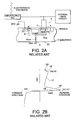
- the second related electrostatic protection circuit uses a parasitic thyrister 2 which is laterally directed, as illustrated in FIG. 2 A.
- FIG. 1 C An equivalent circuit of the second related electrostatic protection circuit is illustrated in FIG. 1 C.
- Such a circuit includes a lateral npn-type parasitic bipolar transistor 21 , a vertical pnp-type parasitic bipolar transistor, a resistor Rnw of an n-well region, and a substrate resistor Rsub of a p-type semiconductor substrate 22 , as illustrated in FIGS. 2A and 2C.
- the current-voltage characteristics of the equivalent circuit are shown in FIG. 2 B.
- the electrostatic protection principle of the second related electrostatic protection circuit using a parasitic thyrister is almost the same as the above-mentioned electrostatic protection principle of the first related electrostatic protection circuit using the parasitic bipolar transistor.
- the static electricity is discharged to the ground by the forward characteristics of an n+p junction between an n+ layer of an electrode C side and the p-type semiconductor substrate 22 .
- the reverse current of the n+p junction is gradually increased, as illustrated in FIG. 2 B.
- the reverse current flows into the substrate resistor Rsub, and the potential of the base electrode B is increased by a voltage drop ( 15 ′).
- the lateral npn-type parasitic bipolar transistor 21 is turned on by the increase of the potential of the base electrode B.
- the lateral thyrister 2 is turned on by a positive feedback operation of a pair of lateral and vertical transistors.
- the n+p junction of the lateral npn-type parasitic bipolar transistor 21 is almost broken down near the first trigger potential (Vt 1 , It 1 ) in FIG. 2 B.
- the device is irreversibly changed by high-temperature heat and is thereby broken ( 19 ′).
- the semiconductor device has been further reduced in size with micropatterning due to recent progress in technology.
- the semiconductor device becomes ever more sensitive with micropatterning.
- semiconductor devices are often broken by a low voltage.
- the thickness of the gate insulating film of MOS devices has been thinned to about 4 nm, while the breakdown voltage of the gate insulating film has been reduced to about 7 V in CMOS devices which are super-micropatterned.
- the semiconductor device may be broken by the static electricity before the electrostatic protection circuit is operated (triggered).
- an electrostatic protection circuit having an operation voltage (trigger voltage) depending on a low breakdown voltage of the compact semiconductor device must be developed and produced.
- the first object is to provide an electrostatic protection device or circuit which operates at a low voltage, which is not higher than the breakdown voltage of the internal circuit, on the condition that the voltage falls within such a range that is not lower than the operation voltage of the internal circuit.
- An electrostatic protection device includes a parasitic bipolar transistor and a trigger device.
- the trigger device is provided adjacent to the parasitic bipolar transistor and injects charges generated by static electricity into a base region of the parasitic bipolar transistor.
- the trigger device injects the charges generated by the static electricity into the base region of the parasitic bipolar transistor. Consequently, the operation voltage (namely, trigger voltage) of the parasitic bipolar transistor advantageously is effectively reduced.
- the trigger device has an insulating film. In this condition, the charges generated by the static electricity are passed through the insulating film by a tunnel effect, and are injected into the base region of the parasitic bipolar transistor.
- the charges are shielded by the insulating film of the trigger device at a low voltage.
- the charges are passed by the tunnel effect at a high voltage to flow into the base electrode of the parasitic bipolar transistor.
- a gate electrode is formed on a semiconductor substrate via a gate insulating film. Moreover, a device isolation layer is formed on the semiconductor substrate of the peripheral portion of the gate electrode.
- a trench as a device isolation layer is formed. Thereby, the number of minority carriers collected to an inversion layer 41 on a surface of the semiconductor substrate becomes low (namely, the minority carriers are short). In consequence, a depletion layer 42 must be extended to compensate for the shortage of the minority carriers.
- the increase of the voltage is used for an increase of a voltage applied to the semiconductor substrate from a voltage Vs 1 to Vs 2 , and is not used for an increase of a voltage Vox applied to the gate insulating film.
- the voltage Vox applied to the gate insulating film is saturated, and a tunnel current depending on the voltage Vox and passing through the gate insulating film is also saturated.
- the trench may be filled in with insulators, such as SiO9.
- a semiconductor region having a polarity opposite to the polarity of the semiconductor substrate may be formed.
- a low-resistance layer is preferably formed in the semiconductor substrate.
- the gate insulating film can be advantageously prevented from being broken.
- a tunnel current passing through the gate insulating film can be induced along the low-resistance layer.
- concentration of the tunnel current can be effectively adjusted at a single point. Further, diffusion of the tunnel current into a predetermined region can be advantageously adjusted.
- the capacitor device preferably has a diode connected in parallel to the gate electrode.
- the reverse current of the diode and the tunnel current are effectively added to each other to flow into the semiconductor substrate.
- the parasitic bipolar transistor is triggered by injecting trigger currents of one or more trigger devices.
- a decrease in operation voltage (namely, a trigger voltage) of the parasitic bipolar transistor depending on the characteristics of the specific trigger elements can be advantageously achieved.
- the parasitic bipolar transistor and the trigger device are arranged such that an adjacent area of the parasitic bipolar transistor and the trigger device is increased.
- the trigger current can be accurately and readily injected into the base electrode of the parasitic bipolar transistor. In consequence, a waste current is advantageously prevented from flowing.
- the semiconductor device according to this invention is strong against static electricity because its internal circuit is protected by the electrostatic protection circuit.
- FIG. 1A is a sectional view of a first related electrostatic protection device or circuit
- FIG. 1B is a graph showing the current-voltage characteristics of a first related electrostatic protection device or circuit
- FIG. 1C is a circuit diagram showing an equivalent circuit of a first related electrostatic protection circuit
- FIG. 2A is a sectional view of a second related electrostatic protection device or circuit
- FIG. 2B is a graph showing the current-voltage characteristics of a second related electrostatic protection device or circuit
- FIG. 2C is a circuit diagram showing an equivalent circuit of a second related electrostatic protection circuit
- FIG. 3A is a sectional view showing an electrostatic protection device (including a capacitor device) according to a first embodiment of this invention
- FIG. 3B is a graph showing the current-voltage characteristic of the capacitor device according to a first embodiment of this invention.
- FIGS. 4A and 4B are band diagrams showing the characteristics of a capacitor device
- FIG. 5A is a sectional view showing an electrostatic protection device or circuit according to a second embodiment of this invention.
- FIG. 5B is a graph showing the current-voltage characteristics of the electrostatic protection device or circuit according to a second embodiment of this invention.
- FIG. 6A is a sectional view showing an electrostatic protection device or circuit according to a third embodiment of this invention.
- FIG. 6B is a graph showing the current-voltage characteristics of the electrostatic protection device or circuit according to a third embodiment of this invention.
- FIG. 7A is a circuit diagram showing an equivalent circuit of an electrostatic protection device or circuit according to a second embodiment of this invention.
- FIG. 7B is a circuit diagram showing an equivalent circuit of an electrostatic protection device or circuit according to a third embodiment of this invention.
- FIG. 8 is a diagram showing an electrostatic protection device or circuit according to a fourth embodiment of this invention.
- FIG. 9 is a diagram showing a device arrangement of an electrostatic protection circuit according to a fifth embodiment of this invention.
- An electrostatic protection device or circuit according to the first embodiment includes a MOS device 3 (namely, a capacitor device), as illustrated in FIG. 3 A.
- a MOS device 3 namely, a capacitor device
- a silicon oxide insulating film 32 is formed on a p-type semiconductor substrate 34
- a gate electrode 31 is formed on the silicon oxide insulating film 32 .
- trenches 33 are formed in the p-type semiconductor substrate 34 to surround the peripheral portion of the gate electrode 31 , and each of the trenches is filled in with a silicon oxide insulator.
- an n+ layer is buried adjacent to the gate electrode 31 to form a parasitic n+p diode, and the n+ electrode is connected to the gate electrode 31 through a conductive line.
- a current value is increased from about 4 V by a tunnel current Im.
- a current obtained by adding the tunnel current Im and the reverse current Ir flows into the substrate resistor Rsub of the p-type semiconductor substrate 34 .
- the capacitor device 3 of the first embodiment effectively prevents this phenomenon by arranging a device isolation layer (namely, the trench 33 ).
- the graph shifts parallel to the abscissa as indicated by a broken line 3 f , and only the voltage applied to the p-type semiconductor substrate 34 is continuously increased while the current is saturated. In consequence, the insulating film is irreversibly changed by high-temperature heat and is broken ( 3 g ).
- the diode is connected to the MOS device in parallel.
- an increase in voltage is limited depending on the characteristics of the diode indicated by a broken line 3 d at a voltage higher than the breakdown voltage of the diode.
- the reverse current Ir flows into the substrate resistor Rsub of the p-type semiconductor substrate 34 .
- the MOS device and the diode are coupled to each other in parallel in the first embodiment. Consequently, the graph 3 a indicated by a solid line in FIG. 3B showing the current-voltage characteristics is obtained by adding the broken line 3 f and the broken line 3 d to each other.
- an insulating film breakdown 3 c of the MOS device 3 a breakdown 3 g of the semiconductor substrate 34 of the MOS device 3 , and a breakdown 3 e of the diode can each be prevented.
- a capacitor device 3 is formed at an adjacent position of a n-MOSFET 1 serving as an electrostatic protection device on a p-type semiconductor substrate 51 of the n-MOSFET 1 .
- the capacitor device 3 has the same structure as the capacitor device 3 illustrated in FIG. 3A according to the first embodiment.
- the electrostatic protection device is connected between an input/output pad and an internal CMOS circuit, and is coupled to the ground.
- the n+ electrode of the parasitic n+p diode of the capacitor device 3 is shared by an electrode S formed on the n+ layer of the n-MOSFET 1 .
- this circuit diagram is shown in FIG. 7 A.
- an npn-type parasitic bipolar transistor 11 is triggered by only the reverse current Ir.
- the electrostatic protection device utilizes the tunnel current Im as a trigger current. Consequently, a decrease 53 of trigger voltage Vt 1 can be achieved, as illustrated in FIG. 5 B.
- the normal operation voltage of the internal CMOS circuit is equal to 3.3 V
- the thickness and the breakdown voltage of the gate insulating film are equal to 8 nm and 10 V, respectively.
- a base potential required to turn on the parasitic bipolar transistor 11 namely, the potential difference between the substrate resistances Rsub, is equal to 0.8 V.
- the film thickness of the recent gate insulating film is changed to 4 nm.
- the gate insulating film breakdown voltage is decreased to 7 V when the film thickness of the gate insulating film becomes 4 nm, and the recent gate insulating film is broken before the electrostatic protection device is triggered in the conventional n-MOSFET 1 .
- n-MOSFET 1 utilized the same manufacturing line as that for an n-MOSFET used in the internal CMOS circuit, and the capacitor device 3 could also be manufactured by the use of the conventional manufacturing step.
- the electrostatic protection device according to the second embodiment When the electrostatic protection device according to the second embodiment was applied to a semiconductor device, the applied voltage exceeded a normal operation voltage of 3.3 V of the internal CMOS circuit by the electrostatic discharge.
- the capacitor device 3 began to cause the tunnel current to flow into the base electrode B of the parasitic bipolar transistor.
- the potential difference between the substrate resistors Rsub became 0.8 V, and the parasitic bipolar transistor 11 was turned on.
- the capacitor device 3 of the first embodiment is arranged adjacent to a lateral thyrister 2 formed in a p-type substrate 61 .
- the circuit diagram of the electrostatic protection device is shown in FIG. 7 B.
- a parasitic bipolar transistor 21 is triggered by only a reverse current Ir.
- the electrostatic protection device uses a tunnel current Im as a trigger current.
- a decrease 63 of a trigger voltage Vt 1 can be achieved, as shown in FIG. 6 B.
- a tunnel current Im flowing into the ground without passing through a substrate resistor Rsub is decreased in the electrostatic protection device according to the second embodiment.
- a high-concentration low-resistance layer 81 is formed in a p-type semiconductor substrate 51 .
- the low-resistance layer 81 is formed in a such a range that a tunnel current Im is introduced to a base electrode B of a parasitic bipolar transistor 11 .
- the low-resistance layer 81 is formed in an area away from a region surrounded by a trench 33 which is under a silicon oxide insulating film 32 and which generates a depletion layer in application to a position immediately before the base electrode B of the npn-type parasitic bipolar transistor 11 .
- the low-resistance layer 81 is not formed in the region in which the depletion layer is generated in application.
- the low-resistance layer 81 is not formed in the region of the substrate resistor Rsub. This reason will be explained as follows.
- the low-resistance layer 81 formed in the region decreases the resistance of the substrate resistor Rsub. Further, it is difficult to increase the voltage of the base electrode B. As a result, a trigger voltage Vt 1 of the electrostatic protection device is increased.
- the low-resistance layer 81 can also be applied to the electrostatic protection device according to the third embodiment, and the tunnel current 62 flowing into the ground without passing through the substrate resistor Rsub is reduced.
- parasitic bipolar transistors and trigger elements are arranged such that the adjacent areas of the parasitic bipolar transistors and trigger devices are increased.
- parasitic bipolar transistors and trigger devices are alternately arranged in a grating form.
- the parasitic bipolar transistors are arranged in four directions of one trigger element. Consequently, the incidence of waste tunnels, i.e., tunnel currents that do not flow into the base electrode B of the parasitic bipolar transistor, is effectively reduced.
- the trigger devices are arranged in the four directions of one parasitic bipolar transistor. Thereby, a trigger current flowing into the base electrode B of the parasitic bipolar transistor and flowing in the substrate resistor Rsub is increased. As a result, a trigger voltage Vt 1 of the electrostatic protection circuit is efficiently decreased.
- resistor layers may be branched toward the base electrodes B of the four parasitic bipolar transistors adjacent to one trigger device.
- the trigger voltage of the electrostatic protection device (element) can be efficiently decreased.
- an economical electrostatic protection device in which a conventional electrostatic protection device manufacturing method, can be directly used without any change.
- an electrostatic protection device is not self-broken by an increase in applied voltage.
- a tunnel current can reliably flow as a trigger current into the base electrode or the substrate resistor of a parasitic bipolar transistor to more efficiently decrease the trigger current.
Abstract
Description
Claims (5)
Applications Claiming Priority (2)
| Application Number | Priority Date | Filing Date | Title |
|---|---|---|---|
| JP11-143747 | 1999-05-24 | ||
| JP14374799A JP3314760B2 (en) | 1999-05-24 | 1999-05-24 | Electrostatic protection element, electrostatic protection circuit, and semiconductor device |
Publications (1)
| Publication Number | Publication Date |
|---|---|
| US6512663B1 true US6512663B1 (en) | 2003-01-28 |
Family
ID=15346085
Family Applications (1)
| Application Number | Title | Priority Date | Filing Date |
|---|---|---|---|
| US09/576,777 Expired - Lifetime US6512663B1 (en) | 1999-05-24 | 2000-05-23 | Electrostatic protection device and electrostatic protection circuit |
Country Status (2)
| Country | Link |
|---|---|
| US (1) | US6512663B1 (en) |
| JP (1) | JP3314760B2 (en) |
Cited By (1)
| Publication number | Priority date | Publication date | Assignee | Title |
|---|---|---|---|---|
| US20140027871A1 (en) * | 2012-07-30 | 2014-01-30 | International Business Machines Corporation | Charge sensors using inverted lateral bipolar junction transistors |
Families Citing this family (3)
| Publication number | Priority date | Publication date | Assignee | Title |
|---|---|---|---|---|
| JP4980575B2 (en) * | 2005-03-30 | 2012-07-18 | ラピスセミコンダクタ株式会社 | Electrostatic protection circuit and semiconductor device including the electrostatic protection circuit |
| JP4625738B2 (en) * | 2005-09-02 | 2011-02-02 | 株式会社東芝 | Semiconductor device and manufacturing method thereof |
| JP4789717B2 (en) * | 2006-07-03 | 2011-10-12 | 阪和電子工業株式会社 | Method for measuring characteristic impedance of electrostatic discharge protection circuit and apparatus for realizing the measurement. |
Citations (15)
| Publication number | Priority date | Publication date | Assignee | Title |
|---|---|---|---|---|
| JPS5640279A (en) | 1979-09-10 | 1981-04-16 | Mitsubishi Electric Corp | Semiconductor integrated circuit |
| JPS5799776A (en) | 1980-12-12 | 1982-06-21 | Toshiba Corp | Semiconductor device |
| US5079608A (en) * | 1990-11-06 | 1992-01-07 | Harris Corporation | Power MOSFET transistor circuit with active clamp |
| US5173755A (en) * | 1989-05-12 | 1992-12-22 | Western Digital Corporation | Capacitively induced electrostatic discharge protection circuit |
| US5182220A (en) * | 1992-04-02 | 1993-01-26 | United Microelectronics Corporation | CMOS on-chip ESD protection circuit and semiconductor structure |
| US5264723A (en) * | 1992-04-09 | 1993-11-23 | At&T Bell Laboratories | Integrated circuit with MOS capacitor for improved ESD protection |
| US5291051A (en) * | 1992-09-11 | 1994-03-01 | National Semiconductor Corporation | ESD protection for inputs requiring operation beyond supply voltages |
| JPH07244991A (en) | 1994-03-01 | 1995-09-19 | Sony Corp | Floating gate type non-volatile semiconductor storage device |
| US5528188A (en) * | 1995-03-13 | 1996-06-18 | International Business Machines Corporation | Electrostatic discharge suppression circuit employing low-voltage triggering silicon-controlled rectifier |
| US5574621A (en) * | 1995-03-27 | 1996-11-12 | Motorola, Inc. | Integrated circuit capacitor having a conductive trench |
| US5581101A (en) * | 1995-01-03 | 1996-12-03 | International Business Machines Corporation | FET and/or bipolar devices formed in thin vertical silicon on insulator (SOI) structures |
| US5625522A (en) * | 1994-08-29 | 1997-04-29 | Cypress Semiconductor Corp. | Apparatus for smart power supply ESD protection structure |
| JPH09223748A (en) | 1995-12-14 | 1997-08-26 | Nec Corp | Semiconductor device |
| JPH10189876A (en) | 1996-12-25 | 1998-07-21 | Hitachi Ltd | Semiconductor integrated circuit device and its manufacture |
| JPH1187631A (en) | 1997-09-09 | 1999-03-30 | Nec Corp | Semiconductor device |
-
1999
- 1999-05-24 JP JP14374799A patent/JP3314760B2/en not_active Expired - Fee Related
-
2000
- 2000-05-23 US US09/576,777 patent/US6512663B1/en not_active Expired - Lifetime
Patent Citations (15)
| Publication number | Priority date | Publication date | Assignee | Title |
|---|---|---|---|---|
| JPS5640279A (en) | 1979-09-10 | 1981-04-16 | Mitsubishi Electric Corp | Semiconductor integrated circuit |
| JPS5799776A (en) | 1980-12-12 | 1982-06-21 | Toshiba Corp | Semiconductor device |
| US5173755A (en) * | 1989-05-12 | 1992-12-22 | Western Digital Corporation | Capacitively induced electrostatic discharge protection circuit |
| US5079608A (en) * | 1990-11-06 | 1992-01-07 | Harris Corporation | Power MOSFET transistor circuit with active clamp |
| US5182220A (en) * | 1992-04-02 | 1993-01-26 | United Microelectronics Corporation | CMOS on-chip ESD protection circuit and semiconductor structure |
| US5264723A (en) * | 1992-04-09 | 1993-11-23 | At&T Bell Laboratories | Integrated circuit with MOS capacitor for improved ESD protection |
| US5291051A (en) * | 1992-09-11 | 1994-03-01 | National Semiconductor Corporation | ESD protection for inputs requiring operation beyond supply voltages |
| JPH07244991A (en) | 1994-03-01 | 1995-09-19 | Sony Corp | Floating gate type non-volatile semiconductor storage device |
| US5625522A (en) * | 1994-08-29 | 1997-04-29 | Cypress Semiconductor Corp. | Apparatus for smart power supply ESD protection structure |
| US5581101A (en) * | 1995-01-03 | 1996-12-03 | International Business Machines Corporation | FET and/or bipolar devices formed in thin vertical silicon on insulator (SOI) structures |
| US5528188A (en) * | 1995-03-13 | 1996-06-18 | International Business Machines Corporation | Electrostatic discharge suppression circuit employing low-voltage triggering silicon-controlled rectifier |
| US5574621A (en) * | 1995-03-27 | 1996-11-12 | Motorola, Inc. | Integrated circuit capacitor having a conductive trench |
| JPH09223748A (en) | 1995-12-14 | 1997-08-26 | Nec Corp | Semiconductor device |
| JPH10189876A (en) | 1996-12-25 | 1998-07-21 | Hitachi Ltd | Semiconductor integrated circuit device and its manufacture |
| JPH1187631A (en) | 1997-09-09 | 1999-03-30 | Nec Corp | Semiconductor device |
Non-Patent Citations (1)
| Title |
|---|
| N. Weste et al. Principles of CMOS VLSI Design, 1985, Addison-Wesley Co., pp. 96-98. * |
Cited By (4)
| Publication number | Priority date | Publication date | Assignee | Title |
|---|---|---|---|---|
| US20140027871A1 (en) * | 2012-07-30 | 2014-01-30 | International Business Machines Corporation | Charge sensors using inverted lateral bipolar junction transistors |
| US9040929B2 (en) * | 2012-07-30 | 2015-05-26 | International Business Machines Corporation | Charge sensors using inverted lateral bipolar junction transistors |
| US9170338B2 (en) | 2012-07-30 | 2015-10-27 | Globalfoundries Inc | Charge sensors using inverted lateral bipolar junction transistors |
| US9377543B2 (en) | 2012-07-30 | 2016-06-28 | Globalfoundries Inc. | Charge sensors using inverted lateral bipolar junction transistors |
Also Published As
| Publication number | Publication date |
|---|---|
| JP3314760B2 (en) | 2002-08-12 |
| JP2000332131A (en) | 2000-11-30 |
Similar Documents
| Publication | Publication Date | Title |
|---|---|---|
| US8842400B2 (en) | Initial-on SCR device on-chip ESD protection | |
| US6750515B2 (en) | SCR devices in silicon-on-insulator CMOS process for on-chip ESD protection | |
| US6538266B2 (en) | Protection device with a silicon-controlled rectifier | |
| US7479414B2 (en) | Electrostatic discharge protection device for digital circuits and for applications with input/output bipolar voltage much higher than the core circuit power supply | |
| US7355252B2 (en) | Electrostatic discharge protection device and method of fabricating the same | |
| US5751042A (en) | Internal ESD protection circuit for semiconductor devices | |
| US20040027745A1 (en) | Drain-extended MOS ESD protection structure | |
| JPH0240221B2 (en) | ||
| US5336908A (en) | Input EDS protection circuit | |
| JPH0151070B2 (en) | ||
| US20070284665A1 (en) | Electrostatic discharge protection device | |
| US7323752B2 (en) | ESD protection circuit with floating diffusion regions | |
| US6570226B1 (en) | Device and circuit for electrostatic discharge and overvoltage protection applications | |
| US7462885B2 (en) | ESD structure for high voltage ESD protection | |
| US6476422B1 (en) | Electrostatic discharge protection circuit with silicon controlled rectifier characteristics | |
| KR101414777B1 (en) | Electrostatic discharge protection devices and methods for protecting semiconductor devices against electrostatic discharge events | |
| JP3317345B2 (en) | Semiconductor device | |
| US6512663B1 (en) | Electrostatic protection device and electrostatic protection circuit | |
| JP3479012B2 (en) | Electrostatic protection circuit and semiconductor device | |
| US6288884B1 (en) | MOS buffer immun to ESD damage | |
| US7126168B1 (en) | Silicon controlled rectifier structures with reduced turn on times | |
| KR100200303B1 (en) | Electrostatic discharge protection circuit for semiconductor device and manufacturing method thereof | |
| JPH07263633A (en) | Static electricity-proof discharge protector of semiconductor device | |
| US7075156B1 (en) | Collector structure for electrostatic discharge protection circuits | |
| KR20030051388A (en) | Polysilicon bounded snapback device |
Legal Events
| Date | Code | Title | Description |
|---|---|---|---|
| AS | Assignment |
Owner name: NEC CORPORATION, JAPAN Free format text: ASSIGNMENT OF ASSIGNORS INTEREST;ASSIGNOR:OKUSHIMA, MOTOTSUGU;REEL/FRAME:010820/0624 Effective date: 20000518 |
|
| STCF | Information on status: patent grant |
Free format text: PATENTED CASE |
|
| AS | Assignment |
Owner name: NEC ELECTRONICS CORPORATION, JAPAN Free format text: ASSIGNMENT OF ASSIGNORS INTEREST;ASSIGNOR:NEC CORPORATION;REEL/FRAME:013736/0321 Effective date: 20021101 |
|
| FPAY | Fee payment |
Year of fee payment: 4 |
|
| FPAY | Fee payment |
Year of fee payment: 8 |
|
| AS | Assignment |
Owner name: RENESAS ELECTRONICS CORPORATION, JAPAN Free format text: CHANGE OF NAME;ASSIGNOR:NEC ELECTRONICS CORPORATION;REEL/FRAME:025375/0959 Effective date: 20100401 |
|
| FPAY | Fee payment |
Year of fee payment: 12 |
|
| AS | Assignment |
Owner name: RENESAS ELECTRONICS CORPORATION, JAPAN Free format text: CHANGE OF ADDRESS;ASSIGNOR:RENESAS ELECTRONICS CORPORATION;REEL/FRAME:044928/0001 Effective date: 20150806 |