US6508062B2 - Thermal exchanger for a wafer chuck - Google Patents
Thermal exchanger for a wafer chuck Download PDFInfo
- Publication number
- US6508062B2 US6508062B2 US09/775,382 US77538201A US6508062B2 US 6508062 B2 US6508062 B2 US 6508062B2 US 77538201 A US77538201 A US 77538201A US 6508062 B2 US6508062 B2 US 6508062B2
- Authority
- US
- United States
- Prior art keywords
- manifold
- thermo
- fins
- electric device
- assembly
- Prior art date
- Legal status (The legal status is an assumption and is not a legal conclusion. Google has not performed a legal analysis and makes no representation as to the accuracy of the status listed.)
- Expired - Fee Related
Links
- 238000000034 method Methods 0.000 claims abstract description 32
- 239000004065 semiconductor Substances 0.000 claims abstract description 9
- 230000006854 communication Effects 0.000 claims description 15
- 238000004891 communication Methods 0.000 claims description 15
- 239000004020 conductor Substances 0.000 claims description 7
- 239000007788 liquid Substances 0.000 claims description 7
- 239000000956 alloy Substances 0.000 claims description 4
- 229910045601 alloy Inorganic materials 0.000 claims description 4
- 238000001816 cooling Methods 0.000 claims description 4
- 239000011888 foil Substances 0.000 claims description 3
- 238000010438 heat treatment Methods 0.000 claims description 3
- 239000000853 adhesive Substances 0.000 claims description 2
- 230000001070 adhesive effect Effects 0.000 claims description 2
- 229910052738 indium Inorganic materials 0.000 claims description 2
- APFVFJFRJDLVQX-UHFFFAOYSA-N indium atom Chemical compound [In] APFVFJFRJDLVQX-UHFFFAOYSA-N 0.000 claims description 2
- 230000006903 response to temperature Effects 0.000 claims 1
- 239000007789 gas Substances 0.000 description 15
- NJPPVKZQTLUDBO-UHFFFAOYSA-N novaluron Chemical compound C1=C(Cl)C(OC(F)(F)C(OC(F)(F)F)F)=CC=C1NC(=O)NC(=O)C1=C(F)C=CC=C1F NJPPVKZQTLUDBO-UHFFFAOYSA-N 0.000 description 12
- 238000005219 brazing Methods 0.000 description 5
- 230000000694 effects Effects 0.000 description 3
- 238000005240 physical vapour deposition Methods 0.000 description 3
- 230000005465 channeling Effects 0.000 description 2
- 238000005229 chemical vapour deposition Methods 0.000 description 2
- 230000001276 controlling effect Effects 0.000 description 2
- 239000000463 material Substances 0.000 description 2
- 238000010926 purge Methods 0.000 description 2
- 230000004044 response Effects 0.000 description 2
- 125000006850 spacer group Chemical group 0.000 description 2
- 239000000758 substrate Substances 0.000 description 2
- XLYOFNOQVPJJNP-UHFFFAOYSA-N water Substances O XLYOFNOQVPJJNP-UHFFFAOYSA-N 0.000 description 2
- RYGMFSIKBFXOCR-UHFFFAOYSA-N Copper Chemical group [Cu] RYGMFSIKBFXOCR-UHFFFAOYSA-N 0.000 description 1
- 230000005679 Peltier effect Effects 0.000 description 1
- XUIMIQQOPSSXEZ-UHFFFAOYSA-N Silicon Chemical compound [Si] XUIMIQQOPSSXEZ-UHFFFAOYSA-N 0.000 description 1
- 230000007175 bidirectional communication Effects 0.000 description 1
- 229910052802 copper Inorganic materials 0.000 description 1
- 239000010949 copper Substances 0.000 description 1
- 238000000151 deposition Methods 0.000 description 1
- 230000008021 deposition Effects 0.000 description 1
- 230000005684 electric field Effects 0.000 description 1
- 238000009413 insulation Methods 0.000 description 1
- 230000001105 regulatory effect Effects 0.000 description 1
- 230000000284 resting effect Effects 0.000 description 1
- 238000000926 separation method Methods 0.000 description 1
- 229910052710 silicon Inorganic materials 0.000 description 1
- 239000010703 silicon Substances 0.000 description 1
- 238000004513 sizing Methods 0.000 description 1
- 238000003860 storage Methods 0.000 description 1
Images


Classifications
-
- H—ELECTRICITY
- H01—ELECTRIC ELEMENTS
- H01L—SEMICONDUCTOR DEVICES NOT COVERED BY CLASS H10
- H01L21/00—Processes or apparatus adapted for the manufacture or treatment of semiconductor or solid state devices or of parts thereof
- H01L21/67—Apparatus specially adapted for handling semiconductor or electric solid state devices during manufacture or treatment thereof; Apparatus specially adapted for handling wafers during manufacture or treatment of semiconductor or electric solid state devices or components ; Apparatus not specifically provided for elsewhere
- H01L21/67005—Apparatus not specifically provided for elsewhere
- H01L21/67011—Apparatus for manufacture or treatment
- H01L21/67098—Apparatus for thermal treatment
- H01L21/67103—Apparatus for thermal treatment mainly by conduction
-
- F—MECHANICAL ENGINEERING; LIGHTING; HEATING; WEAPONS; BLASTING
- F25—REFRIGERATION OR COOLING; COMBINED HEATING AND REFRIGERATION SYSTEMS; HEAT PUMP SYSTEMS; MANUFACTURE OR STORAGE OF ICE; LIQUEFACTION SOLIDIFICATION OF GASES
- F25B—REFRIGERATION MACHINES, PLANTS OR SYSTEMS; COMBINED HEATING AND REFRIGERATION SYSTEMS; HEAT PUMP SYSTEMS
- F25B21/00—Machines, plants or systems, using electric or magnetic effects
- F25B21/02—Machines, plants or systems, using electric or magnetic effects using Peltier effect; using Nernst-Ettinghausen effect
- F25B21/04—Machines, plants or systems, using electric or magnetic effects using Peltier effect; using Nernst-Ettinghausen effect reversible
-
- H—ELECTRICITY
- H01—ELECTRIC ELEMENTS
- H01L—SEMICONDUCTOR DEVICES NOT COVERED BY CLASS H10
- H01L21/00—Processes or apparatus adapted for the manufacture or treatment of semiconductor or solid state devices or of parts thereof
- H01L21/67—Apparatus specially adapted for handling semiconductor or electric solid state devices during manufacture or treatment thereof; Apparatus specially adapted for handling wafers during manufacture or treatment of semiconductor or electric solid state devices or components ; Apparatus not specifically provided for elsewhere
- H01L21/67005—Apparatus not specifically provided for elsewhere
- H01L21/67011—Apparatus for manufacture or treatment
- H01L21/67098—Apparatus for thermal treatment
- H01L21/67109—Apparatus for thermal treatment mainly by convection
-
- H—ELECTRICITY
- H01—ELECTRIC ELEMENTS
- H01L—SEMICONDUCTOR DEVICES NOT COVERED BY CLASS H10
- H01L21/00—Processes or apparatus adapted for the manufacture or treatment of semiconductor or solid state devices or of parts thereof
- H01L21/67—Apparatus specially adapted for handling semiconductor or electric solid state devices during manufacture or treatment thereof; Apparatus specially adapted for handling wafers during manufacture or treatment of semiconductor or electric solid state devices or components ; Apparatus not specifically provided for elsewhere
- H01L21/683—Apparatus specially adapted for handling semiconductor or electric solid state devices during manufacture or treatment thereof; Apparatus specially adapted for handling wafers during manufacture or treatment of semiconductor or electric solid state devices or components ; Apparatus not specifically provided for elsewhere for supporting or gripping
- H01L21/687—Apparatus specially adapted for handling semiconductor or electric solid state devices during manufacture or treatment thereof; Apparatus specially adapted for handling wafers during manufacture or treatment of semiconductor or electric solid state devices or components ; Apparatus not specifically provided for elsewhere for supporting or gripping using mechanical means, e.g. chucks, clamps or pinches
- H01L21/68714—Apparatus specially adapted for handling semiconductor or electric solid state devices during manufacture or treatment thereof; Apparatus specially adapted for handling wafers during manufacture or treatment of semiconductor or electric solid state devices or components ; Apparatus not specifically provided for elsewhere for supporting or gripping using mechanical means, e.g. chucks, clamps or pinches the wafers being placed on a susceptor, stage or support
- H01L21/68785—Apparatus specially adapted for handling semiconductor or electric solid state devices during manufacture or treatment thereof; Apparatus specially adapted for handling wafers during manufacture or treatment of semiconductor or electric solid state devices or components ; Apparatus not specifically provided for elsewhere for supporting or gripping using mechanical means, e.g. chucks, clamps or pinches the wafers being placed on a susceptor, stage or support characterised by the mechanical construction of the susceptor, stage or support
Definitions
- the present invention relates generally to method and apparatus for semiconductor processing, and more particularly to thermal exchanger assembly for a wafer chuck assembly.
- the wafer In semiconductor wafer processing, the wafer is conventionally maintained within a desired temperature range. Though this may involve regulating temperature in a process chamber, it conventionally involves controlling the temperature of the wafer.
- thermo-electric devices are disposed under a support surface supporting the wafer in an oriented planar array.
- temperature gradients form between such thermo-electric devices and cause variation across the wafer.
- a planar array of thermo-electric devices is limited to surface area under the support surface.
- thermo-electric device attaching at least one thermo-electric device to a stem, which is attached to a platen.
- stem length may be limited in some process chambers. Accordingly, it would be desirable to provide a solution having more available surface area within a confined volume for attaching at least one thermo-electric device.
- An aspect of the present invention comprises a thermal exchanger assembly for a wafer chuck assembly.
- the thermal exchanger assembly comprises a first manifold having a first set of radially positioned fins, and a second manifold having a second set of radially positioned fins.
- the first and second set of radially positioned fins interleaved with one another to provide spaced-apart pairs of fins.
- At least one thermo-electric device is alternately located between and in thermal communication with the pairs of fins.
- Another aspect of the present invention is a thermal exchanger assembly at least partially located in a process chamber of a processing system.
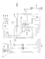
- FIG. 1 depicts a schematic and cross-sectional view of an exemplary portion of a processing system having a thermal exchanger assembly
- FIGS. 2A through 2C depict cross-sectional views of an exemplary portion of an embodiment of a thermal exchanger assembly in accordance with aspects of the present invention
- FIG. 3 depicts a perspective view of a thermo-electric device that may be used in the thermal exchanger assembly of FIG. 2;
- FIG. 3A depicts a surface plan view of an alternate embodiment of the thermo-electric device of FIG. 3;
- FIG. 4 depicts a plan and cross-sectional view illustrating radial positioning of an exemplary portion of the thermal exchanger assembly of FIG. 2;
- FIG. 4A depicts a perspective view illustrating electrical connections for an exemplary portion of the embodiment of the thermal exchanger assembly of FIG. 2 C.
- Process system 99 comprises process chamber 100 .
- Process chamber 100 generally houses a support pedestal 150 .
- Susceptor or wafer chuck assembly 10 comprises a portion of support pedestal 150 .
- Wafer chuck assembly 10 may be an electrostatic chuck.
- Wafer chuck assembly 10 which is used to support a substrate such as a wafer 11 within process chamber 100 .
- wafer 11 can be heated or cooled to some desired temperature or within some desired temperature range.
- wafer 11 refers to any work piece upon which film processing is performed.
- wafer 11 may be a silicon semiconductor wafer, or other material layer, which has been formed on wafer 11 .
- thermo-electric devices 20 In chamber 100 , wafer chuck assembly 10 is heated or cooled by applying an electric current from power supply 106 to thermo-electric devices 20 (shown in FIG. 2 ). Thermo-electric devices 20 (shown in FIG. 2) draw (subtract) or supply (add) thermal energy depending on direction of current flow of power supply 106 . Accordingly, a thermo-electric device may take advantage of a Peltier effect. Wafer 11 may be heated or cooled to within a desired process temperature range of about ⁇ 40° C. to about 200° C., subject to properties of materials used in assembly 98 of FIG. 2 .
- wafer chuck assembly 10 may be heated or cooled by supplying a thermal medium, such as a liquid through piping 421 from pump and reservoir 420 .
- a thermal medium such as a liquid through piping 421 from pump and reservoir 420 .
- Pump and reservoir 420 may be coupled via piping 423 to a heater or chiller 422 for supplying or removing thermal energy to such a thermal medium.
- Temperature sensor 29 such as a thermocouple, may be attached to or embedded in wafer chuck assembly 10 to monitor temperature in a conventional manner. For example, measured temperature may be used in a feedback loop to control electric current applied to thermo-electric devices 20 from power supply 106 , such that wafer temperature can be maintained or controlled at a desired temperature or within a desired temperature range suitable for a process application.
- Control unit 110 may be used to receive a signal from temperature sensor 29 and control power supply 106 in response.
- Vacuum pump 102 is used to evacuate process gases from process chamber 100 and to help maintain a desired pressure or desired pressure within a pressure range inside chamber 100 .
- Orifice 120 through a wall of chamber 100 is used to introduce process gases into process chamber 100 . Sizing of orifice 120 conventionally depends on the size of process chamber 100 .
- Chamber 100 is coupled to gas panel 130 via orifice 120 in part by valve 125 .
- Gas panel 130 is configured to receive and then provide a resultant process gas from two or more gas sources 135 , 136 to process chamber 100 through orifice 120 and valve 125 .
- Gas panel 130 is further configured to receive and then provide a purge gas from purge gas source 138 to process chamber 100 through orifice 120 and valve 125 .
- Control unit 110 such as a programmed personal computer, work station computer, and the like, is configured to control flow of various process gases through gas panel 130 as well as valve 125 during different stages of a wafer process sequence.
- control unit 110 comprises central processing unit (CPU) 112 , support circuitry 114 , and memory 116 containing associated control software 113 .
- control unit 110 may be configured to be responsible for automated control of other activities used in wafer processing—such as wafer transport, temperature control, chamber evacuation, among other activities, some of which are described elsewhere herein.
- Control unit 110 may be one of any form of general purpose computer processor that can be used in an industrial setting for controlling various chambers and sub-processors.
- CPU 112 may use any suitable memory 116 , such as random access memory, read only memory, floppy disk drive, hard disk, or any other form of digital storage, local or remote.
- Various support circuits may be coupled to CPU 112 for supporting system 10 .
- Software routines 113 as required may be stored in memory 116 or executed by a second computer processor that is remotely located (not shown). Bi-directional communications between control unit 110 and various other components of wafer processing system 10 are handled through numerous signal cables collectively referred to as signal buses 118 , some of which are illustrated in FIG. 1 .
- Process system 99 comprises RF power supplies 410 and 412 , showerhead 400 , gas source 405 , and matching network(s) 411 .
- process system 99 may be configured for physical vapor deposition (PVD) or chemical vapor deposition (CVD). More particularly, process system 99 may be used for PVD “subzero” deposition of copper, where wafer chuck assembly 10 is cooled for cooling substrate structure 11 to temperatures from about ⁇ 20° C. to about 0° C.
- showerhead 400 and wafer support pedestal 150 provide in part spaced apart electrodes. An electric field may be generated between these electrodes to ignite a process gas introduced into chamber 100 to provide plasma 405 .
- pedestal 150 is coupled to a source of radio frequency (RF) power source 412 through a matching network 411 , which in turn may be coupled to control unit 110 .
- RF power source 410 may be coupled to showerhead 400 and matching network 411 , which in turn may be coupled to control unit 110 .
- matching network 411 may comprise different circuits for RF power sources 410 and 412 , and both RF power sources 410 and 412 may be coupled to showerhead 400 and pedestal 150 , respectively.
- Wafer chuck assembly 10 comprises a platen 12 , a thermal exchanger assembly 98 , and a manifold 15 .
- Manifold 15 comprises at least one conduit 16 having at least one inlet and at least one outlet. However, manifold 15 may comprise one or more inlets and a plurality of outlets and conduits 16 . Manifold 15 may be a separate work piece as illustratively shown in FIGS. 2A and 2B, or integrally formed with manifold 14 , as illustratively shown in FIG. 2 C.
- Thermal exchanger assembly 98 comprises a manifold 14 , a plurality of thermo-electric devices 20 , and a manifold 13 .
- Manifold 14 comprises base 14 B and a plurality of fins 14 F.
- Manifold 13 comprises base 13 B and a plurality of fins 13 F. Fins 13 F and 14 F mate with one another in an interleaving of fins to provide spaced-apart pairs of fins 13 F and 14 F.
- Disposed at least partially in alternating regions between fins 13 F and 14 F is at least one thermo-electric device 20 . Accordingly, a plurality radially disposed thermo-electric devices 20 may be located in alternating gaps between fins 13 F and 14 F. Between combinations of fins 13 F, 14 F and at least one thermo-electric device 20 are gaps 21 . Gaps 21 provide thermal conductivity separation regions between such combinations for channeling thermal exchange between manifold 13 and manifold 14 .
- Thermo-electric device 20 may be sufficiently tall to prevent manifolds 13 and 14 from touching one another, as illustratively shown in FIG. 2C; otherwise, manifolds 13 and 14 may be in direct thermal communication and thermal energy channeling through thermo-electric devices 20 would quantitatively be reduced. Because of such height of thermo-electric devices 20 , gaps 17 form between base member portions of manifolds 13 and 14 and upper fin portions of fins 14 F and 13 F, respectively, separating manifolds 13 and 14 from touching one another. Gaps 17 may be considered as a portion of gaps 21 . However, having thermo-electric devices 20 sufficiently tall to prevent manifolds 13 and 14 from touching may provide an unwanted thermal conduction path longitudinally through thermo-electric devices 20 .
- thermo-electric devices 20 in this embodiment should have thermal insulation at distal longitudinal ends.
- Arrows 18 , in FIG. 2C, illustratively show a thermal conduction path for heating platen 12 and thus heating wafer 11 .
- Arrows 18 , in FIG. 2B, illustratively show a thermal conduction path for removing heat from platen 12 and thus cooling platen 12 and in turn wafer 11 .
- thermo-electric devices 20 are not so tall as to prevent direct contact between manifolds 13 and 14 .
- Temporary spacers 17 T may be used for positioning manifold 13 with respect to manifold 14 , and later those temporary spacers 17 T may be removed.
- thermo-electric device 20 comprises plates 31 and Peltier device 22 .
- Peltier device 22 may be coupled to a power supply via wires 24 and 25 .
- Thermo-electric device 20 has upper and lower surfaces 28 , side surfaces 26 , and inner surface 27 .
- Thermally conductive material 23 is disposed on side surfaces 26 .
- Thermally conductive material 23 may be selected from a thermally conductive adhesive or a brazing alloy. With respect to a brazing alloy, a brazing foil may be used. Such a brazing foil may be pressure sensitive so less temperature is needed to braze thermo-electric device 20 to fins 13 F and 14 F.
- a suitable brazing alloy may comprise indium.
- Thermo-electric device 20 may be shaped for radial disposition, as is illustratively shown in the top view of FIG. 3 A.
- thermo-electric devices 20 alternate in sequence and are radially disposed on or over manifold base 14 B.
- Thermo-electric devices 20 may be wired together, as illustratively shown with respect to wire 24 .
- tubular core 14 C shown in FIG. 4A, may be disposed in region 97 of manifold base 14 B.
- Tubular core 14 C comprises conductive rings 34 and 35 .
- Electrical contacts 24 and 25 of thermo-electric devices 20 may be put in contact with an exterior surface of conductive rings 34 and 35 , respectively, and wires 24 and 25 may be in contact with an interior surface of conductive rings 34 and 35 for electrical connection to a power supply.
Abstract
A thermal exchanger assembly for a wafer chuck and method of use therefor is disclosed. More particularly, complimentary manifolds, each having a plurality of fins, are positioned with respect to one another to provide interleaved spaced-apart fins. At least one thermo-electric device is disposed between alternating pairs of fins. The thermo-electric device is coupled to the fins to provide a thermally conductive path from one manifold to the other through the thermo-electric device. The thermal exchanger assembly may be located in a process chamber for processing a wafer, including but not limited to a semiconductor wafer.
Description
1. Field of the Invention
The present invention relates generally to method and apparatus for semiconductor processing, and more particularly to thermal exchanger assembly for a wafer chuck assembly.
2. Description of the Background Art
In semiconductor wafer processing, the wafer is conventionally maintained within a desired temperature range. Though this may involve regulating temperature in a process chamber, it conventionally involves controlling the temperature of the wafer.
Others have addressed wafer temperature control by providing chilled water through a wafer support pedestal. By cooling the wafer support pedestal, the wafer resting on a wafer chuck is cooled as well. However, this approach is time consuming, and conventionally response times are limited to approximately 2 minutes per degree. Because of the time required for chilled water to take effect, compensation times may be too long for rapid thermal processing or other processing causing rapid wafer temperature changes.
Others have suggested using thermo-electric devices. These devices are disposed under a support surface supporting the wafer in an oriented planar array. However, temperature gradients form between such thermo-electric devices and cause variation across the wafer. Additionally, a planar array of thermo-electric devices is limited to surface area under the support surface.
To address these limitations, others have suggested attaching at least one thermo-electric device to a stem, which is attached to a platen. However, stem length may be limited in some process chambers. Accordingly, it would be desirable to provide a solution having more available surface area within a confined volume for attaching at least one thermo-electric device.
An aspect of the present invention comprises a thermal exchanger assembly for a wafer chuck assembly. The thermal exchanger assembly comprises a first manifold having a first set of radially positioned fins, and a second manifold having a second set of radially positioned fins. The first and second set of radially positioned fins interleaved with one another to provide spaced-apart pairs of fins. At least one thermo-electric device is alternately located between and in thermal communication with the pairs of fins.
Another aspect of the present invention is a thermal exchanger assembly at least partially located in a process chamber of a processing system. These and other aspects of the present invention will be more apparent from the following description.
The teachings of the present invention can be readily understood by considering the following detailed description in conjunction with the accompanying drawings, in which:
FIG. 1 depicts a schematic and cross-sectional view of an exemplary portion of a processing system having a thermal exchanger assembly;
FIGS. 2A through 2C (collectively referred to as FIG. 2) depict cross-sectional views of an exemplary portion of an embodiment of a thermal exchanger assembly in accordance with aspects of the present invention;
FIG. 3 depicts a perspective view of a thermo-electric device that may be used in the thermal exchanger assembly of FIG. 2;
FIG. 3A depicts a surface plan view of an alternate embodiment of the thermo-electric device of FIG. 3;
FIG. 4 depicts a plan and cross-sectional view illustrating radial positioning of an exemplary portion of the thermal exchanger assembly of FIG. 2; and
FIG. 4A depicts a perspective view illustrating electrical connections for an exemplary portion of the embodiment of the thermal exchanger assembly of FIG. 2C.
Process System
Referring to FIG. 1, there is illustratively shown an exemplary embodiment of a process system 99 in accordance with an aspect of the present invention. Process system 99 comprises process chamber 100. Process chamber 100 generally houses a support pedestal 150. Susceptor or wafer chuck assembly 10 comprises a portion of support pedestal 150. Wafer chuck assembly 10 may be an electrostatic chuck. Wafer chuck assembly 10, which is used to support a substrate such as a wafer 11 within process chamber 100. Depending on process requirements, wafer 11 can be heated or cooled to some desired temperature or within some desired temperature range. For purposes of clarity, wafer 11 refers to any work piece upon which film processing is performed. Depending on processing stage, wafer 11 may be a silicon semiconductor wafer, or other material layer, which has been formed on wafer 11.
In chamber 100, wafer chuck assembly 10 is heated or cooled by applying an electric current from power supply 106 to thermo-electric devices 20 (shown in FIG. 2). Thermo-electric devices 20 (shown in FIG. 2) draw (subtract) or supply (add) thermal energy depending on direction of current flow of power supply 106. Accordingly, a thermo-electric device may take advantage of a Peltier effect. Wafer 11 may be heated or cooled to within a desired process temperature range of about −40° C. to about 200° C., subject to properties of materials used in assembly 98 of FIG. 2.
Additionally, wafer chuck assembly 10 may be heated or cooled by supplying a thermal medium, such as a liquid through piping 421 from pump and reservoir 420. Pump and reservoir 420 may be coupled via piping 423 to a heater or chiller 422 for supplying or removing thermal energy to such a thermal medium.
Conventionally, pedestal 150 is coupled to a source of radio frequency (RF) power source 412 through a matching network 411, which in turn may be coupled to control unit 110. Alternatively, RF power source 410 may be coupled to showerhead 400 and matching network 411, which in turn may be coupled to control unit 110. Moreover, matching network 411 may comprise different circuits for RF power sources 410 and 412, and both RF power sources 410 and 412 may be coupled to showerhead 400 and pedestal 150, respectively.
Wafer Chuck Assembly
Referring to FIG. 2, there is illustratively shown several exemplary embodiments of wafer chuck assembly 10. Wafer chuck assembly 10 comprises a platen 12, a thermal exchanger assembly 98, and a manifold 15.
Thermo-electric device 20 may be sufficiently tall to prevent manifolds 13 and 14 from touching one another, as illustratively shown in FIG. 2C; otherwise, manifolds 13 and 14 may be in direct thermal communication and thermal energy channeling through thermo-electric devices 20 would quantitatively be reduced. Because of such height of thermo-electric devices 20, gaps 17 form between base member portions of manifolds 13 and 14 and upper fin portions of fins 14F and 13F, respectively, separating manifolds 13 and 14 from touching one another. Gaps 17 may be considered as a portion of gaps 21. However, having thermo-electric devices 20 sufficiently tall to prevent manifolds 13 and 14 from touching may provide an unwanted thermal conduction path longitudinally through thermo-electric devices 20. Accordingly, thermo-electric devices 20 in this embodiment should have thermal insulation at distal longitudinal ends. Arrows 18, in FIG. 2C, illustratively show a thermal conduction path for heating platen 12 and thus heating wafer 11. Arrows 18, in FIG. 2B, illustratively show a thermal conduction path for removing heat from platen 12 and thus cooling platen 12 and in turn wafer 11.
In FIG. 2B and in FIG. 2A, thermo-electric devices 20 are not so tall as to prevent direct contact between manifolds 13 and 14. Temporary spacers 17T may be used for positioning manifold 13 with respect to manifold 14, and later those temporary spacers 17T may be removed.
Referring to FIG. 3, there is illustratively shown a perspective view of thermo-electric device 20. Thermo-electric device 20 comprises plates 31 and Peltier device 22. Peltier device 22 may be coupled to a power supply via wires 24 and 25. Thermo-electric device 20 has upper and lower surfaces 28, side surfaces 26, and inner surface 27. Thermally conductive material 23 is disposed on side surfaces 26. Thermally conductive material 23 may be selected from a thermally conductive adhesive or a brazing alloy. With respect to a brazing alloy, a brazing foil may be used. Such a brazing foil may be pressure sensitive so less temperature is needed to braze thermo-electric device 20 to fins 13F and 14F. A suitable brazing alloy may comprise indium. Thermo-electric device 20 may be shaped for radial disposition, as is illustratively shown in the top view of FIG. 3A.
Referring to FIG. 4, there is illustratively shown a cross-sectional and top plan view of an exemplary portion of thermal exchanger assembly 98. As illustratively shown, fins 13F, gaps 21, fins 14F, and thermo-electric devices 20 alternate in sequence and are radially disposed on or over manifold base 14B. Thermo-electric devices 20 may be wired together, as illustratively shown with respect to wire 24. Alternatively, tubular core 14C, shown in FIG. 4A, may be disposed in region 97 of manifold base 14B.
Referring to FIG. 4A, there is illustratively shown a perspective view of tubular core 14C. Tubular core 14C comprises conductive rings 34 and 35. Electrical contacts 24 and 25 of thermo-electric devices 20 may be put in contact with an exterior surface of conductive rings 34 and 35, respectively, and wires 24 and 25 may be in contact with an interior surface of conductive rings 34 and 35 for electrical connection to a power supply.
Although several preferred embodiments, which incorporate the teachings of the present invention, have been shown and described in detail, those skilled in the art can readily devise many other varied embodiments that still incorporate these teachings.
Claims (21)
1. A thermal exchanger assembly for a wafer chuck assembly, comprising:
a first manifold having a first set of radially positioned fins;
a second manifold having a second set of radially positioned fins;
the first set of radially positioned fins and the second set of radially positioned fins configured to interleave with one another to provide spaced-apart pairs of fins; and
at least one thermo-electric device alternately located between and in thermal communication with the pairs of fins.
2. The thermal exchanger assembly of claim 1 , wherein the at least one thermo-electric device comprises a Peltier device.
3. The thermal exchanger assembly of claim 1 , further comprising a third manifold, the third manifold formed with at least one conduit having an inlet and an outlet configured for transporting a thermal medium in and out of the third manifold.
4. The thermal exchanger assembly of claim 1 , wherein the second manifold is formed with at least one conduit having an inlet and an outlet configured for transporting a thermal medium in and out of the second manifold.
5. The thermal exchanger assembly of claim 1 , wherein the at least one thermo-electric device is electrically coupled to a power supply.
6. An apparatus for a wafer chuck assembly, comprising:
a platen;
a first manifold in thermal communication with the platen, the first manifold having base and a first set of radially positioned fins extending from the base;
a second manifold having a base and a second set of radially positioned fins extending from the base;
the first set of radially position fins and the second set of radially positioned fins configured to interleave with one another to provide spaced-apart pairs of fins;
at least one thermo-electric device alternately located between and in thermal communication with the pairs of fins; and
a thermally conductive material located between the at least one thermo-electric device and each fin of the pairs of fins in thermal communication with the thermo-electric device, the thermally conductive material for attaching the pairs of fins to the at least one thermo-electric device.
7. The assembly of claim 6 , further comprising a third manifold in thermal communication with the second manifold, the third manifold formed with a plurality of conduits for transporting a liquid.
8. The assembly of claim 7 , wherein the second manifold comprises a tubular core, the tubular core comprising conductive rings configured for electrical contact with at least one thermo electric device.
9. The assembly of claim 8 , further comprising a thermo-couple in thermal communication with the platen.
10. The assembly of claim 9 , wherein the thermally conductive material is a thermally conductive adhesive.
11. The assembly of claim 9 , wherein the thermally conductive material is a braze alloy.
12. The assembly of claim 9 , wherein the thermally conductive material is a foil comprising indium.
13. A semiconductor processing system, comprising:
a chamber;
a wafer chuck assembly at least partially located within the chamber, the wafer chuck assembly comprising:
a platen;
a first manifold in thermal communication with the platen, the first manifold having base and a first set of radially positioned fins extending from the base;
a second manifold having a base and a second set of radially positioned fins extending from the base;
the first set of radially position fins and the second set of radially positioned fins configured to interleave with one another to provide spaced-apart pairs of fins;
at least one thermo-electric device alternately located between and in thermal communication with the pairs of fins;
a thermo-couple in thermal communication with the wafer chuck assembly;
a power supply electrically coupled to the at least one thermo-electric device; and
a controller operatively coupled to the thermo-couple and to the power supply, the controller configured to regulate the power supply in response to temperature sensed by the thermo-couple.
14. The system of claim 13 , further comprising:
a third manifold in thermal communication with the second manifold, the third manifold formed with conduits for transporting a liquid; and
a pump and reservoir coupled to conduits of the third manifold for circulating the liquid.
15. The system of claim 14 , further comprising a radio frequency source electrically coupled to the wafer chuck assembly.
16. The system of claim 14 , further comprising:
a showerhead at least partially disposed within the chamber; and
a radio frequency source electrically coupled to the showerhead.
17. The system of claim 14 , further comprising:
a vacuum system coupled to the chamber for removing gas; and
at least one gas source coupled to the chamber for providing gas thereto.
18. The system of claim 13 , further comprising:
a third manifold in thermal communication with the second manifold, the third manifold formed with conduits for transporting a liquid;
a pump and reservoir coupled to conduits of the third manifold for circulating the liquid;
a first radio frequency source electrically coupled to the wafer chuck assembly;
a showerhead at least partially disposed within the chamber;
a second radio frequency source electrically coupled to the showerhead;
a vacuum system coupled to the chamber for removing gas; and
at least one gas source coupled to the chamber for providing gas thereto.
19. The system of claim 18 , further comprising a chiller operatively coupled to the pump and reservoir for providing the liquid thereto.
20. A method of processing a semiconductor wafer, comprising:
locating the semiconductor wafer on a wafer chuck assembly in a chamber, the wafer in thermal communication with a platen of the wafer chuck assembly; and
cooling the platen by supplying an electrical current to at least one thermo-electric device located in the wafer chuck assembly, the at least one thermo-electric device radially disposed between fins of respective upper and lower manifolds.
21. A method of processing a semiconductor wafer, comprising:
locating the semiconductor wafer on a wafer chuck assembly in a chamber, the wafer in thermal communication with a platen of the wafer chuck assembly; and
heating the platen by supplying an electrical current to at least one thermo-electric device located in the wafer chuck assembly, the at least one thermo-electric device radially disposed between fins of respective upper and lower manifolds.
Priority Applications (1)
| Application Number | Priority Date | Filing Date | Title |
|---|---|---|---|
| US09/775,382 US6508062B2 (en) | 2001-01-31 | 2001-01-31 | Thermal exchanger for a wafer chuck |
Applications Claiming Priority (1)
| Application Number | Priority Date | Filing Date | Title |
|---|---|---|---|
| US09/775,382 US6508062B2 (en) | 2001-01-31 | 2001-01-31 | Thermal exchanger for a wafer chuck |
Publications (2)
| Publication Number | Publication Date |
|---|---|
| US20020100282A1 US20020100282A1 (en) | 2002-08-01 |
| US6508062B2 true US6508062B2 (en) | 2003-01-21 |
Family
ID=25104225
Family Applications (1)
| Application Number | Title | Priority Date | Filing Date |
|---|---|---|---|
| US09/775,382 Expired - Fee Related US6508062B2 (en) | 2001-01-31 | 2001-01-31 | Thermal exchanger for a wafer chuck |
Country Status (1)
| Country | Link |
|---|---|
| US (1) | US6508062B2 (en) |
Cited By (10)
| Publication number | Priority date | Publication date | Assignee | Title |
|---|---|---|---|---|
| US20030015290A1 (en) * | 2001-07-17 | 2003-01-23 | Canon Kabushiki Kaisha | Substrate processing apparatus, substrate processing method, and exposure apparatus |
| US20030021671A1 (en) * | 2001-07-27 | 2003-01-30 | Canon Kabushiki Kaisha | Substrate processing apparatus, method of controlling substrate, and exposure apparatus |
| US6805748B1 (en) | 1999-10-19 | 2004-10-19 | Canon Kabushiki Kaisha | Substrate processing system with load-lock chamber |
| US20050016183A1 (en) * | 2003-07-25 | 2005-01-27 | Kabushiki Kaisha Toshiba | Thermoelectric device |
| WO2005074450A2 (en) * | 2004-01-30 | 2005-08-18 | Tokyo Electron Limited | Substrate holder having a fluid gap and method of fabricating the substrate holder |
| US20070283709A1 (en) * | 2006-06-09 | 2007-12-13 | Veeco Instruments Inc. | Apparatus and methods for managing the temperature of a substrate in a high vacuum processing system |
| US20080093057A1 (en) * | 2006-08-18 | 2008-04-24 | Samsung Electronics Co., Ltd. | Cooling apparatus having an auxiliary chiller, and an apparatus and method of fabricating a semiconductor device using the same |
| US9224626B2 (en) | 2012-07-03 | 2015-12-29 | Watlow Electric Manufacturing Company | Composite substrate for layered heaters |
| US20170092514A1 (en) * | 2011-08-30 | 2017-03-30 | Watlow Electric Manufacturing Company | High definition heater system having a fluid medium |
| US9673077B2 (en) | 2012-07-03 | 2017-06-06 | Watlow Electric Manufacturing Company | Pedestal construction with low coefficient of thermal expansion top |
Families Citing this family (2)
| Publication number | Priority date | Publication date | Assignee | Title |
|---|---|---|---|---|
| US7731798B2 (en) * | 2004-12-01 | 2010-06-08 | Ultratech, Inc. | Heated chuck for laser thermal processing |
| KR20170127724A (en) * | 2016-05-12 | 2017-11-22 | 삼성전자주식회사 | Plasma processing apparatus |
Citations (17)
| Publication number | Priority date | Publication date | Assignee | Title |
|---|---|---|---|---|
| US3719052A (en) | 1971-05-04 | 1973-03-06 | G White | Vacuum system cold trap |
| US4432635A (en) * | 1979-12-20 | 1984-02-21 | Censor Patent-Und Versuchs-Anstalt | Temperature-controlled support for semiconductor wafer |
| US5029445A (en) | 1990-03-19 | 1991-07-09 | Higgins Robert W | Thermal electric cooling system for liquids |
| US5061630A (en) | 1988-05-13 | 1991-10-29 | Agrogen Foundation, Seyffer & Co. & Ulrich C. Knopf | Laboratory apparatus for optional temperature-controlled heating and cooling |
| US5134436A (en) | 1987-12-10 | 1992-07-28 | Canon Kabushiki Kaisha | Exposure control method for adjusting the temperature of a workpiece holding chuck attracting surface based on memorized data |
| US5154661A (en) | 1991-07-10 | 1992-10-13 | Noah Precision, Inc. | Thermal electric cooling system and method |
| US5269146A (en) | 1990-08-28 | 1993-12-14 | Kerner James M | Thermoelectric closed-loop heat exchange system |
| US5450726A (en) | 1993-07-16 | 1995-09-19 | Noah Precision, Inc. | Thermal electric air cooling apparatus and method |
| US5456081A (en) * | 1994-04-01 | 1995-10-10 | International Business Machines Corporation | Thermoelectric cooling assembly with optimized fin structure for improved thermal performance and manufacturability |
| US5522215A (en) | 1993-10-18 | 1996-06-04 | Dainippon Screen Mfg. Co., Ltd. | Substrate cooling apparatus |
| US5613364A (en) | 1995-10-06 | 1997-03-25 | Pou, Inc. | Compact replaceable temperature control module |
| US5667622A (en) | 1995-08-25 | 1997-09-16 | Siemens Aktiengesellschaft | In-situ wafer temperature control apparatus for single wafer tools |
| US5671117A (en) | 1994-02-28 | 1997-09-23 | Applied Materials Inc. | Electrostatic chuck |
| US5728253A (en) | 1993-03-04 | 1998-03-17 | Tokyo Electron Limited | Method and devices for detecting the end point of plasma process |
| US5740016A (en) | 1996-03-29 | 1998-04-14 | Lam Research Corporation | Solid state temperature controlled substrate holder |
| US5802856A (en) * | 1996-07-31 | 1998-09-08 | Stanford University | Multizone bake/chill thermal cycling module |
| US5996353A (en) * | 1998-05-21 | 1999-12-07 | Applied Materials, Inc. | Semiconductor processing system with a thermoelectric cooling/heating device |
-
2001
- 2001-01-31 US US09/775,382 patent/US6508062B2/en not_active Expired - Fee Related
Patent Citations (17)
| Publication number | Priority date | Publication date | Assignee | Title |
|---|---|---|---|---|
| US3719052A (en) | 1971-05-04 | 1973-03-06 | G White | Vacuum system cold trap |
| US4432635A (en) * | 1979-12-20 | 1984-02-21 | Censor Patent-Und Versuchs-Anstalt | Temperature-controlled support for semiconductor wafer |
| US5134436A (en) | 1987-12-10 | 1992-07-28 | Canon Kabushiki Kaisha | Exposure control method for adjusting the temperature of a workpiece holding chuck attracting surface based on memorized data |
| US5061630A (en) | 1988-05-13 | 1991-10-29 | Agrogen Foundation, Seyffer & Co. & Ulrich C. Knopf | Laboratory apparatus for optional temperature-controlled heating and cooling |
| US5029445A (en) | 1990-03-19 | 1991-07-09 | Higgins Robert W | Thermal electric cooling system for liquids |
| US5269146A (en) | 1990-08-28 | 1993-12-14 | Kerner James M | Thermoelectric closed-loop heat exchange system |
| US5154661A (en) | 1991-07-10 | 1992-10-13 | Noah Precision, Inc. | Thermal electric cooling system and method |
| US5728253A (en) | 1993-03-04 | 1998-03-17 | Tokyo Electron Limited | Method and devices for detecting the end point of plasma process |
| US5450726A (en) | 1993-07-16 | 1995-09-19 | Noah Precision, Inc. | Thermal electric air cooling apparatus and method |
| US5522215A (en) | 1993-10-18 | 1996-06-04 | Dainippon Screen Mfg. Co., Ltd. | Substrate cooling apparatus |
| US5671117A (en) | 1994-02-28 | 1997-09-23 | Applied Materials Inc. | Electrostatic chuck |
| US5456081A (en) * | 1994-04-01 | 1995-10-10 | International Business Machines Corporation | Thermoelectric cooling assembly with optimized fin structure for improved thermal performance and manufacturability |
| US5667622A (en) | 1995-08-25 | 1997-09-16 | Siemens Aktiengesellschaft | In-situ wafer temperature control apparatus for single wafer tools |
| US5613364A (en) | 1995-10-06 | 1997-03-25 | Pou, Inc. | Compact replaceable temperature control module |
| US5740016A (en) | 1996-03-29 | 1998-04-14 | Lam Research Corporation | Solid state temperature controlled substrate holder |
| US5802856A (en) * | 1996-07-31 | 1998-09-08 | Stanford University | Multizone bake/chill thermal cycling module |
| US5996353A (en) * | 1998-05-21 | 1999-12-07 | Applied Materials, Inc. | Semiconductor processing system with a thermoelectric cooling/heating device |
Non-Patent Citations (1)
| Title |
|---|
| U.S. Ser. No. 09/707,043, filed Nov. 6, 2000. |
Cited By (21)
| Publication number | Priority date | Publication date | Assignee | Title |
|---|---|---|---|---|
| US6805748B1 (en) | 1999-10-19 | 2004-10-19 | Canon Kabushiki Kaisha | Substrate processing system with load-lock chamber |
| US20030015290A1 (en) * | 2001-07-17 | 2003-01-23 | Canon Kabushiki Kaisha | Substrate processing apparatus, substrate processing method, and exposure apparatus |
| US20030021671A1 (en) * | 2001-07-27 | 2003-01-30 | Canon Kabushiki Kaisha | Substrate processing apparatus, method of controlling substrate, and exposure apparatus |
| US7024266B2 (en) * | 2001-07-27 | 2006-04-04 | Canon Kabushiki Kaisha | Substrate processing apparatus, method of controlling substrate, and exposure apparatus |
| US20060142890A1 (en) * | 2001-07-27 | 2006-06-29 | Canon Kabushiki Kaisha | Substrate processing apparatus, method of controlling substrate, and exposure apparatus |
| US20050016183A1 (en) * | 2003-07-25 | 2005-01-27 | Kabushiki Kaisha Toshiba | Thermoelectric device |
| US20070256427A1 (en) * | 2003-07-25 | 2007-11-08 | Kabushiki Kaisha Toshiba | Thermoelectric device |
| US7278199B2 (en) | 2003-07-25 | 2007-10-09 | Kabushiki Kaisha Toshiba | Method of making a thermoelectric device |
| US7024865B2 (en) * | 2003-07-25 | 2006-04-11 | Kabushiki Kaisha Toshiba | Thermoelectric device |
| US20060123799A1 (en) * | 2003-07-25 | 2006-06-15 | Kabushiki Kaisha Toshiba | Thermoelectric device |
| US20070224777A1 (en) * | 2004-01-30 | 2007-09-27 | Tokyo Electron Limited | Substrate Holder Having a Fluid Gap and Method of Fabricating the Substrate Holder |
| WO2005074450A3 (en) * | 2004-01-30 | 2006-02-16 | Tokyo Electron Ltd | Substrate holder having a fluid gap and method of fabricating the substrate holder |
| WO2005074450A2 (en) * | 2004-01-30 | 2005-08-18 | Tokyo Electron Limited | Substrate holder having a fluid gap and method of fabricating the substrate holder |
| CN100452306C (en) * | 2004-01-30 | 2009-01-14 | 东京毅力科创株式会社 | Substrate holder having a fluid gap and method of fabricating the substrate holder |
| US8007591B2 (en) | 2004-01-30 | 2011-08-30 | Tokyo Electron Limited | Substrate holder having a fluid gap and method of fabricating the substrate holder |
| US20070283709A1 (en) * | 2006-06-09 | 2007-12-13 | Veeco Instruments Inc. | Apparatus and methods for managing the temperature of a substrate in a high vacuum processing system |
| US20080093057A1 (en) * | 2006-08-18 | 2008-04-24 | Samsung Electronics Co., Ltd. | Cooling apparatus having an auxiliary chiller, and an apparatus and method of fabricating a semiconductor device using the same |
| US20170092514A1 (en) * | 2011-08-30 | 2017-03-30 | Watlow Electric Manufacturing Company | High definition heater system having a fluid medium |
| US10361103B2 (en) * | 2011-08-30 | 2019-07-23 | Watlow Electric Manufacturing Company | High definition heater system having a fluid medium |
| US9224626B2 (en) | 2012-07-03 | 2015-12-29 | Watlow Electric Manufacturing Company | Composite substrate for layered heaters |
| US9673077B2 (en) | 2012-07-03 | 2017-06-06 | Watlow Electric Manufacturing Company | Pedestal construction with low coefficient of thermal expansion top |
Also Published As
| Publication number | Publication date |
|---|---|
| US20020100282A1 (en) | 2002-08-01 |
Similar Documents
| Publication | Publication Date | Title |
|---|---|---|
| US10879053B2 (en) | Temperature controlled substrate support assembly | |
| JP4481913B2 (en) | Substrate pedestal assembly and processing chamber | |
| US6949722B2 (en) | Method and apparatus for active temperature control of susceptors | |
| CN100440422C (en) | Substrate support having dynamic temperature control | |
| CN106469666B (en) | Base and matrix processing equipment | |
| US6214121B1 (en) | Pedestal with a thermally controlled platen | |
| TWI780597B (en) | Wafer carrier with independent isolated heater zones | |
| US9681497B2 (en) | Multi zone heating and cooling ESC for plasma process chamber | |
| JP5484650B2 (en) | Active cooling of substrate support | |
| US8194384B2 (en) | High temperature electrostatic chuck and method of using | |
| JP2001274231A (en) | Apparatus for controlling temperature in semiconductor processing system | |
| JP7186719B2 (en) | In situ semiconductor processing chamber temperature device | |
| US20070139856A1 (en) | Method and apparatus for controlling temperature of a substrate | |
| JP2008522446A (en) | Method and apparatus for controlling spatial temperature distribution | |
| US6508062B2 (en) | Thermal exchanger for a wafer chuck | |
| KR101039085B1 (en) | Plasma processing apparatus and plasma processing method | |
| TW202141681A (en) | Substrate support | |
| TW202117914A (en) | Substrate support pedestal and plasma processing apparatus |
Legal Events
| Date | Code | Title | Description |
|---|---|---|---|
| AS | Assignment |
Owner name: APPLIED MATERIALS, INC., CALIFORNIA Free format text: ASSIGNMENT OF ASSIGNORS INTEREST;ASSIGNOR:FLANIGAN, ALLEN;REEL/FRAME:011537/0180 Effective date: 20010131 |
|
| FPAY | Fee payment |
Year of fee payment: 4 |
|
| FPAY | Fee payment |
Year of fee payment: 8 |
|
| REMI | Maintenance fee reminder mailed | ||
| LAPS | Lapse for failure to pay maintenance fees | ||
| STCH | Information on status: patent discontinuation |
Free format text: PATENT EXPIRED DUE TO NONPAYMENT OF MAINTENANCE FEES UNDER 37 CFR 1.362 |
|
| FP | Lapsed due to failure to pay maintenance fee |
Effective date: 20150121 |