US6504203B2 - Method of forming a metal-insulator-metal capacitor for dual damascene interconnect processing and the device so formed - Google Patents

Method of forming a metal-insulator-metal capacitor for dual damascene interconnect processing and the device so formed Download PDF

Info

Publication number
US6504203B2
US6504203B2 US09/681,197 US68119701A US6504203B2 US 6504203 B2 US6504203 B2 US 6504203B2 US 68119701 A US68119701 A US 68119701A US 6504203 B2 US6504203 B2 US 6504203B2
Authority
US
United States
Prior art keywords
capacitor
conductive
layer
metal
insulative layer
Prior art date
Legal status (The legal status is an assumption and is not a legal conclusion. Google has not performed a legal analysis and makes no representation as to the accuracy of the status listed.)
Expired - Fee Related
Application number
US09/681,197
Other versions
US20020117703A1 (en
Inventor
Jeffrey P. Gambino
Stephen E. Luce
Thomas L. McDevitt
Henry W. Trombley
Current Assignee (The listed assignees may be inaccurate. Google has not performed a legal analysis and makes no representation or warranty as to the accuracy of the list.)
International Business Machines Corp
Original Assignee
International Business Machines Corp
Priority date (The priority date is an assumption and is not a legal conclusion. Google has not performed a legal analysis and makes no representation as to the accuracy of the date listed.)
Filing date
Publication date
Application filed by International Business Machines Corp filed Critical International Business Machines Corp
Priority to US09/681,197 priority Critical patent/US6504203B2/en
Assigned to INTERNATIONAL BUSINESS MACHINES CORPORATION reassignment INTERNATIONAL BUSINESS MACHINES CORPORATION ASSIGNMENT OF ASSIGNORS INTEREST (SEE DOCUMENT FOR DETAILS). Assignors: HENRY W. TROMBLEY, JEFFREY P. GAMBINO, STEPHEN E. LUCE, THOMAS L. MCDEVITT
Priority to TW091102204A priority patent/TWI224828B/en
Publication of US20020117703A1 publication Critical patent/US20020117703A1/en
Priority to US10/260,613 priority patent/US6762108B2/en
Application granted granted Critical
Publication of US6504203B2 publication Critical patent/US6504203B2/en
Anticipated expiration legal-status Critical
Expired - Fee Related legal-status Critical Current

Links

Images

Classifications

    • HELECTRICITY
    • H01ELECTRIC ELEMENTS
    • H01LSEMICONDUCTOR DEVICES NOT COVERED BY CLASS H10
    • H01L28/00Passive two-terminal components without a potential-jump or surface barrier for integrated circuits; Details thereof; Multistep manufacturing processes therefor
    • H01L28/40Capacitors
    • H01L28/55Capacitors with a dielectric comprising a perovskite structure material
    • HELECTRICITY
    • H01ELECTRIC ELEMENTS
    • H01LSEMICONDUCTOR DEVICES NOT COVERED BY CLASS H10
    • H01L23/00Details of semiconductor or other solid state devices
    • H01L23/52Arrangements for conducting electric current within the device in operation from one component to another, i.e. interconnections, e.g. wires, lead frames
    • H01L23/522Arrangements for conducting electric current within the device in operation from one component to another, i.e. interconnections, e.g. wires, lead frames including external interconnections consisting of a multilayer structure of conductive and insulating layers inseparably formed on the semiconductor body
    • H01L23/5222Capacitive arrangements or effects of, or between wiring layers
    • H01L23/5223Capacitor integral with wiring layers
    • HELECTRICITY
    • H01ELECTRIC ELEMENTS
    • H01LSEMICONDUCTOR DEVICES NOT COVERED BY CLASS H10
    • H01L21/00Processes or apparatus adapted for the manufacture or treatment of semiconductor or solid state devices or of parts thereof
    • H01L21/70Manufacture or treatment of devices consisting of a plurality of solid state components formed in or on a common substrate or of parts thereof; Manufacture of integrated circuit devices or of parts thereof
    • H01L21/71Manufacture of specific parts of devices defined in group H01L21/70
    • H01L21/768Applying interconnections to be used for carrying current between separate components within a device comprising conductors and dielectrics
    • H01L21/76838Applying interconnections to be used for carrying current between separate components within a device comprising conductors and dielectrics characterised by the formation and the after-treatment of the conductors
    • HELECTRICITY
    • H01ELECTRIC ELEMENTS
    • H01LSEMICONDUCTOR DEVICES NOT COVERED BY CLASS H10
    • H01L2924/00Indexing scheme for arrangements or methods for connecting or disconnecting semiconductor or solid-state bodies as covered by H01L24/00
    • H01L2924/0001Technical content checked by a classifier
    • H01L2924/0002Not covered by any one of groups H01L24/00, H01L24/00 and H01L2224/00
    • YGENERAL TAGGING OF NEW TECHNOLOGICAL DEVELOPMENTS; GENERAL TAGGING OF CROSS-SECTIONAL TECHNOLOGIES SPANNING OVER SEVERAL SECTIONS OF THE IPC; TECHNICAL SUBJECTS COVERED BY FORMER USPC CROSS-REFERENCE ART COLLECTIONS [XRACs] AND DIGESTS
    • Y10TECHNICAL SUBJECTS COVERED BY FORMER USPC
    • Y10STECHNICAL SUBJECTS COVERED BY FORMER USPC CROSS-REFERENCE ART COLLECTIONS [XRACs] AND DIGESTS
    • Y10S438/00Semiconductor device manufacturing: process
    • Y10S438/957Making metal-insulator-metal device

Definitions

  • the present invention relates generally to semiconductor processing, and more particularly, to the formation of a capacitor and the capacitor so formed.
  • FIG. 1 shows a structure 10 comprising a first metal wiring layer 11 and a second metal wiring layer 13 .
  • the first metal wiring layer 11 includes an insulative layer 12 having a first via 16 and a pair of first metal lines 18 formed therein.
  • the second metal wiring layer 13 includes an insulative layer 14 having a plurality of second vias 20 and a second metal line 22 formed therein.
  • a capping layer 24 such as SiN, is deposited over the surface of the second metal wiring layer 13 to prevent the material within the second metal line 22 (typically copper), from oxidizing.
  • a first mask (not shown) is used to pattern and etch an opening 26 within the capping layer 24 to expose the second vias 20 in the region where the capacitor is to be formed.
  • a capacitor stack 28 comprising a first electrode layer 30 , a dielectric layer 32 and a second electrode layer 34 , is deposited over the surface of the second metal wiring layer 13 .
  • a second mask (not shown) is deposited over the capacitor stack 28 to pattern and etch the stack 28 as illustrated in FIG. 3 .
  • a third metal wiring layer 35 may be formed over the second metal wiring layer 13 by depositing an insulative layer 36 , such as SiO2, over the structure 10 and planarizing the insulative layer 36 .
  • a plurality of third vias 38 and third metal lines 40 are formed in the insulative layer 36 , as shown in FIG. 4 .
  • the copper within the second metal line 22 and second vias 20 has a faster polish rate than the insulating material of the insulative layer 14 , i.e., SiO2, “dishing” may occur.
  • a portion of the exposed metal line 22 and second vias 20 is removed below the surface of the metal wiring layer 13 , e.g., about 100-500 â, , ⁇ , (FIG. 5 ). This creates corners 42 which are replicated in subsequent layers, e.g., the capping layer 24 and the capacitor stack 28 .
  • the thickness of the layers of the capacitor ( 30 , 32 , 34 ) will be reduced over the corners, particularly along the vertical sidewalls of the capacitor stack 28 , and therefore, are more likely to cause device failures due to shorting.
  • the third vias 38 are simultaneously etched within the insulative layer 36 .
  • the vias 38 over the capacitor 28 need to be etched to a depth less than that of the other vias 38 . Therefore, the vias 38 and capacitor 28 are exposed a prolonged overetch. As a result, the capacitor 28 may be penetrated by the extended overetch, causing the capacitor 28 to be shorted out or damaged.
  • an additional step is required to planarize the material forming the third metal wiring layer 35 following deposition of the insulative layer 36 (typically, SiO2) because the capacitor stack 28 extends vertically above the capping layer 24 , forming a bump or high spot within the insulative layer 36 .
  • the material forming the third metal wiring layer 35 typically, SiO2
  • a first general aspect of the present invention provides a capacitor for a semiconductor device, comprising: a first and a second conductive element formed within a first insulative layer; a first conductive plate formed over the first conductive element; a second insulative layer formed over the first conductive plate; a second conductive plate formed over the second insulative layer; and a conductive layer electrically connecting the second conductive plate and the second conductive element.
  • a second general aspect of the present invention provides a semiconductor device, comprising: a first and a second conductive element formed within a first insulative layer; a capacitor formed over the first conductive element; a spacer formed around the capacitor; and a conductive layer electrically connecting the capacitor and the second conductive element.
  • a third general aspect of the present invention provides a method of forming a capacitor for a semiconductor device, comprising: forming at least a first and a second conductive element within an insulative layer; forming a capacitor over the first conductive element; forming a spacer around the capacitor; and forming a conductive layer electrically connecting the capacitor to the second conductive element.
  • FIG. 1 depicts a related art structure having a capping layer thereon
  • FIG. 2 depicts the related art structure of FIG. 1 having a capacitor stack thereon;
  • FIG. 3 depicts the related art structure of FIG. 2 following patterning and etching of the capacitor stack
  • FIG. 4 depicts the related art structure of FIG. 3 having an additional metal wiring layer formed thereon.
  • FIG. 5 depicts the related art structure of FIG. 3 illustrating a defect formed during processing
  • FIG. 6 depicts a structure in accordance with the present invention
  • FIG. 7 depicts the structure of FIG. 6 having a capacitor stack deposited thereover in accordance with the present invention
  • FIG. 8 depicts the structure of FIG. 7 following patterning and etching of the capacitor stack in accordance with the present invention
  • FIG. 9 depicts the structure of FIG. 8 having a spacer formed around the capacitor stack in accordance with the present invention.
  • FIG. 10 depicts the structure of FIG. 9 having a conductive layer formed thereover in accordance with the present invention.
  • FIG. 6 shows a semiconductor device or structure 100 including a first metal wiring layer 101 formed using conventional semiconductor processing techniques.
  • the first metal wiring layer 101 includes an insulative layer 102 , comprising SiO2, or other similarly used material, having a first conductive element or via 106 and a pair of first conductive or metal lines 108 formed therein.
  • the via 106 is patterned using photolithographic, or other similar processes, and etched using a reactive ion etch (RIE), or other similar process.
  • RIE reactive ion etch
  • the metal lines 108 are patterned using photolithographic, or other similar processes, and etched using a reactive ion etch (RIE), or other similar process.
  • RIE reactive ion etch
  • a conductive material such as W, Al, Ti, TiN, etc.
  • PVD physical vapor deposition
  • CVD chemical vapor deposition
  • the surface of the metal wiring layer 101 is then planarized, using a conventional polishing process, to remove excess conductive material on the surface of the metal wiring layer 101 .
  • a layer of insulative material 104 such as SiO2, or other similarly used material, is then deposited over the surface of the first metal wiring layer 101 .
  • a plurality of second conductive elements or vias 110 and 110 ′ are formed in the insulative layer 104 in a similar manner as the vias 106 in the first metal wiring layer 101 , (wherein the vias 110 , in this example three vias 110 , are formed in a region of the structure 100 beneath the capacitor, described and formed infra, and the vias 110 ′ are formed in a region of the structure 100 separated from the capacitor).
  • the vias 110 , 110 ′ are patterned using photolithographic, or other similar processes and etched to approximately the same depth using a RIE, or other similar etching process.
  • a conductive material such as W, Al, Ti, TiN, etc.
  • a conductive material such as W, Al, Ti, TiN, etc.
  • a capacitor stack 112 is deposited over the surface of the insulative layer 104 , using PVD, CVD, or other similar deposition technique.
  • the capacitor stack 112 comprises a first electrode layer 114 , a dielectric layer 116 and a second electrode layer 118 .
  • the first and second electrode layers 114 , 118 , or electrically conductive plates, are each deposited having a thickness in the range of approximately 10-200 nm, e.g., 100 nm, and comprise TiN, Ti, Ta, TaN, Pt, Al, or other similar material.
  • the dielectric layer 116 is deposited having a thickness in the range of approximately 5-50 nm, e.g., 10 nm, and comprises SiO2, Si3N4, Ta2O5, BaSrTiO3, ZrO2, HfO2, TiO2, or other similar material.
  • the capacitor stack 112 is patterned, using a lithographic or other similar process, and etched, using a RIE or other similar process, to form a capacitor 113 .
  • a RIE or other similar process For instance, an F-based (fluorine based) RIE, Cl-based (chlorine based) RIE, or other similar etch may be used to etch the first and second electrode layers 114 , 118 , and an F-based RIE, or other similar etch, may be used to etch the dielectric layer 116 .
  • a spacer 120 is formed around the perimeter of the capacitor 113 .
  • an insulating material such as SiO2, Si3N4, etc.
  • PECVD plasma enhanced chemical vapor deposition
  • the spacer material is deposited having a thickness in the range of approximately 20-200 nm, e.g., 100 nm.
  • the spacer material is etched, using an F-based RIE, or other similar etching process, to form the spacer 120 covering the vertical walls of the capacitor 113 .
  • a conductive layer or second metal line 122 such as Al, W, Au, silver, or other similar material, is formed over the capacitor 113 , the spacer 120 and the surface of the second insulative layer 104 , such that electrical contact is made between thee second electrode layer 118 and the second via 110 ′, thereby forming a second metal wiring layer 103 .
  • the second metal line 122 is deposited having a thickness in the range of approximately 10-200 nm, e.g., 500 nm, over the surface of the structure 100 . Thereafter, the second metal line 122 is patterned, using a lithographic or other similar process, and etched, using RIE, or other similar process.
  • the second metal line 122 is formed to electrically connect the vias 106 , 110 ′ and first metal line 108 to the second electrode layer 118 of the capacitor 113 . Contact with the first electrode layer 114 , however, would produce a short. Therefore, the spacer 120 prevents the second metal line 122 from contacting the first electrode layer 114 .
  • the present invention overcomes many of the problems associated with the related art. For instance, because the vias 106 , 110 , 110 ′ and the metal lines 108 , 122 are formed of a material that does not oxidize when exposed to air, unlike the copper used in the related art, there is no need for a capping layer. Elimination of the capping layer also eradicates the need for the additional masking step required to pattern and etch an opening within the capping layer prior to the formation of the capacitor.
  • the second metal line 122 is formed on top of the capacitor 113 , the need to form the third metal wiring layer 35 , containing the vias 38 and metal lines 40 necessary to form an electrical connection between the vias 16 , 20 , 38 and metal lines 18 , 24 , 40 of the second metal wiring layer 13 and the capacitor 28 (FIG. 4 ), is eliminated. As a result, the added step of depositing the third metal wiring layer 35 , and planarizing the third metal wiring layer 35 over the capacitor 28 , is no longer needed. Also, because the via 110 ′ is formed of tungsten or aluminum, rather than copper, the via 110 ′ may be wire bonded to the second metal line 122 without forming an additional metal wiring layer.
  • the related art problem associated with etching the third vias 38 and third metal lines 40 within the third metal wiring layer 35 is eliminated.
  • the vias 110 , 110 ′ are formed at approximately the same depth. Accordingly, there is no need to form a third wiring layer 35 , having third vias 38 which are to be etched at different depths (FIG. 4 ).
  • the related art problem of “dishing” is significantly minimized because the material used to form the vias 110 , 110 ′, e.g., tungsten, aluminum, etc., has a polish rate similar to that of the material in the insulative layer 104 , unlike the related art copper. Therefore, the material within the vias 110 , 110 ′ is less likely to be overetched, and partially removed, during planarization.

Abstract

The present invention provides a method of forming a capacitor in a last metal wiring layer, and the structure so formed. The invention further provides a spacer formed around the capacitor to electrically isolate portions of the capacitor

Description

BACKGROUND OF THE INVENTION
1. Technical Field
The present invention relates generally to semiconductor processing, and more particularly, to the formation of a capacitor and the capacitor so formed.
2. Related Art
A conventional method of producing a metal-insulator-metal capacitor using dual damascene processing is illustrated in related art FIGS. 1-5. In particular, FIG. 1 shows a structure 10 comprising a first metal wiring layer 11 and a second metal wiring layer 13. The first metal wiring layer 11 includes an insulative layer 12 having a first via 16 and a pair of first metal lines 18 formed therein. The second metal wiring layer 13 includes an insulative layer 14 having a plurality of second vias 20 and a second metal line 22 formed therein.
A capping layer 24, such as SiN, is deposited over the surface of the second metal wiring layer 13 to prevent the material within the second metal line 22 (typically copper), from oxidizing. A first mask (not shown) is used to pattern and etch an opening 26 within the capping layer 24 to expose the second vias 20 in the region where the capacitor is to be formed.
As shown in FIG. 2, a capacitor stack 28, comprising a first electrode layer 30, a dielectric layer 32 and a second electrode layer 34, is deposited over the surface of the second metal wiring layer 13. A second mask (not shown) is deposited over the capacitor stack 28 to pattern and etch the stack 28 as illustrated in FIG. 3. Following removal of the second mask, a third metal wiring layer 35 may be formed over the second metal wiring layer 13 by depositing an insulative layer 36, such as SiO2, over the structure 10 and planarizing the insulative layer 36. Thereafter, a plurality of third vias 38 and third metal lines 40 are formed in the insulative layer 36, as shown in FIG. 4.
However, there are several disadvantages associated with this method. For instance, because the second vias 20 and second metal lines 22 are typically formed of copper, which cannot be wire bonded, an additional metal wiring layer 35, having aluminum vias 38 and metal lines 40, must be formed over the capacitor stack 28 to make electrical connection.
The use of copper within the second vias 20 and second metal lines 22 also necessitates the use of a capping layer to prevent oxidation, as well as an additional masking step to form the capacitor stack opening in the capping layer 24. This creates additional steps which increase manufacturing time and costs.
Also, because the copper within the second metal line 22 and second vias 20 has a faster polish rate than the insulating material of the insulative layer 14, i.e., SiO2, “dishing” may occur. In other words, during a polishing step used to remove excess copper deposited to form the metal line 22 and vias 20, a portion of the exposed metal line 22 and second vias 20 is removed below the surface of the metal wiring layer 13, e.g., about 100-500 â, , <<, (FIG. 5). This creates corners 42 which are replicated in subsequent layers, e.g., the capping layer 24 and the capacitor stack 28. The thickness of the layers of the capacitor (30, 32, 34) will be reduced over the corners, particularly along the vertical sidewalls of the capacitor stack 28, and therefore, are more likely to cause device failures due to shorting.
In addition, the third vias 38 are simultaneously etched within the insulative layer 36. As illustrated in FIG. 4, the vias 38 over the capacitor 28 need to be etched to a depth less than that of the other vias 38. Therefore, the vias 38 and capacitor 28 are exposed a prolonged overetch. As a result, the capacitor 28 may be penetrated by the extended overetch, causing the capacitor 28 to be shorted out or damaged.
Furthermore, an additional step is required to planarize the material forming the third metal wiring layer 35 following deposition of the insulative layer 36 (typically, SiO2) because the capacitor stack 28 extends vertically above the capping layer 24, forming a bump or high spot within the insulative layer 36.
Therefore, there exists a need in the industry for a method of producing a metal-insulator-metal capacitor, using dual damascene processing, that overcomes these and other problems.
BRIEF SUMMARY OF THE INVENTION
A first general aspect of the present invention provides a capacitor for a semiconductor device, comprising: a first and a second conductive element formed within a first insulative layer; a first conductive plate formed over the first conductive element; a second insulative layer formed over the first conductive plate; a second conductive plate formed over the second insulative layer; and a conductive layer electrically connecting the second conductive plate and the second conductive element.
A second general aspect of the present invention provides a semiconductor device, comprising: a first and a second conductive element formed within a first insulative layer; a capacitor formed over the first conductive element; a spacer formed around the capacitor; and a conductive layer electrically connecting the capacitor and the second conductive element.
A third general aspect of the present invention provides a method of forming a capacitor for a semiconductor device, comprising: forming at least a first and a second conductive element within an insulative layer; forming a capacitor over the first conductive element; forming a spacer around the capacitor; and forming a conductive layer electrically connecting the capacitor to the second conductive element.
The foregoing and other features and advantages of the invention will be apparent from the following more particular description of the embodiments of the invention.
BRIEF DESCRIPTION OF THE SEVERAL VIEWS OF THE DRAWINGS
The embodiments of this invention will be described in detail, with reference to the following figures, wherein like designations denote like elements, and wherein:
FIG. 1 depicts a related art structure having a capping layer thereon;
FIG. 2 depicts the related art structure of FIG. 1 having a capacitor stack thereon;
FIG. 3 depicts the related art structure of FIG. 2 following patterning and etching of the capacitor stack;
FIG. 4 depicts the related art structure of FIG. 3 having an additional metal wiring layer formed thereon.
FIG. 5 depicts the related art structure of FIG. 3 illustrating a defect formed during processing;
FIG. 6 depicts a structure in accordance with the present invention;
FIG. 7 depicts the structure of FIG. 6 having a capacitor stack deposited thereover in accordance with the present invention;
FIG. 8 depicts the structure of FIG. 7 following patterning and etching of the capacitor stack in accordance with the present invention;
FIG. 9 depicts the structure of FIG. 8 having a spacer formed around the capacitor stack in accordance with the present invention; and
FIG. 10 depicts the structure of FIG. 9 having a conductive layer formed thereover in accordance with the present invention.
DETAILED DESCRIPTION OF THE INVENTION Description of the Preferred Embodiment
Although certain embodiments of the present invention will be shown and described in detail, it should be understood that various changes and may be made without departing from the scope of the appended claims. The scope of the present invention will in no way be limited to the number of constituting components, the materials thereof, the shapes thereof, the relative arrangement thereof, etc. Although the drawings are intended to illustrate the present invention, the drawings are not necessarily drawn to scale.
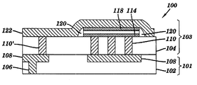
Referring to the drawings, FIG. 6 shows a semiconductor device or structure 100 including a first metal wiring layer 101 formed using conventional semiconductor processing techniques. For instance, the first metal wiring layer 101 includes an insulative layer 102, comprising SiO2, or other similarly used material, having a first conductive element or via 106 and a pair of first conductive or metal lines 108 formed therein. The via 106 is patterned using photolithographic, or other similar processes, and etched using a reactive ion etch (RIE), or other similar process. Likewise, the metal lines 108 are patterned using photolithographic, or other similar processes, and etched using a reactive ion etch (RIE), or other similar process. Thereafter, a conductive material, such as W, Al, Ti, TiN, etc., is deposited, using physical vapor deposition (PVD), chemical vapor deposition (CVD), etc., over the surface of the metal wiring layer 101, filling the vias 106 and the metal lines 108. The surface of the metal wiring layer 101 is then planarized, using a conventional polishing process, to remove excess conductive material on the surface of the metal wiring layer 101.
A layer of insulative material 104, such as SiO2, or other similarly used material, is then deposited over the surface of the first metal wiring layer 101. A plurality of second conductive elements or vias 110 and 110′ are formed in the insulative layer 104 in a similar manner as the vias 106 in the first metal wiring layer 101, (wherein the vias 110, in this example three vias 110, are formed in a region of the structure 100 beneath the capacitor, described and formed infra, and the vias 110′ are formed in a region of the structure 100 separated from the capacitor). For instance, the vias 110, 110′ are patterned using photolithographic, or other similar processes and etched to approximately the same depth using a RIE, or other similar etching process. Thereafter, a conductive material, such as W, Al, Ti, TiN, etc., is deposited, using PVD, CVD, etc., over the surface of the insulative layer 104, filling the vias 110, 110′. The surface of the insulative layer 104 is then planarized, using conventional polishing processes, to remove excess conductive material on the surface of the layer 104.
As illustrated in FIG. 7, a capacitor stack 112 is deposited over the surface of the insulative layer 104, using PVD, CVD, or other similar deposition technique. The capacitor stack 112 comprises a first electrode layer 114, a dielectric layer 116 and a second electrode layer 118. The first and second electrode layers 114, 118, or electrically conductive plates, are each deposited having a thickness in the range of approximately 10-200 nm, e.g., 100 nm, and comprise TiN, Ti, Ta, TaN, Pt, Al, or other similar material. The dielectric layer 116, or electrically insulative layer, is deposited having a thickness in the range of approximately 5-50 nm, e.g., 10 nm, and comprises SiO2, Si3N4, Ta2O5, BaSrTiO3, ZrO2, HfO2, TiO2, or other similar material.
As illustrated in FIG. 8, the capacitor stack 112 is patterned, using a lithographic or other similar process, and etched, using a RIE or other similar process, to form a capacitor 113. For instance, an F-based (fluorine based) RIE, Cl-based (chlorine based) RIE, or other similar etch may be used to etch the first and second electrode layers 114, 118, and an F-based RIE, or other similar etch, may be used to etch the dielectric layer 116.
As shown in FIG. 9, a spacer 120 is formed around the perimeter of the capacitor 113. For example, an insulating material, such as SiO2, Si3N4, etc., is deposited over the surface of the structure 100 using plasma enhanced chemical vapor deposition (PECVD), or other similar process. The spacer material is deposited having a thickness in the range of approximately 20-200 nm, e.g., 100 nm. Thereafter, the spacer material is etched, using an F-based RIE, or other similar etching process, to form the spacer 120 covering the vertical walls of the capacitor 113.
As illustrated in FIG. 10, a conductive layer or second metal line 122, such as Al, W, Au, silver, or other similar material, is formed over the capacitor 113, the spacer 120 and the surface of the second insulative layer 104, such that electrical contact is made between thee second electrode layer 118 and the second via 110′, thereby forming a second metal wiring layer 103. For instance, the second metal line 122 is deposited having a thickness in the range of approximately 10-200 nm, e.g., 500 nm, over the surface of the structure 100. Thereafter, the second metal line 122 is patterned, using a lithographic or other similar process, and etched, using RIE, or other similar process.
The second metal line 122 is formed to electrically connect the vias 106, 110′ and first metal line 108 to the second electrode layer 118 of the capacitor 113. Contact with the first electrode layer 114, however, would produce a short. Therefore, the spacer 120 prevents the second metal line 122 from contacting the first electrode layer 114.
By forming the capacitor stack 112 in the last metal wiring layer 103, the present invention overcomes many of the problems associated with the related art. For instance, because the vias 106, 110, 110′ and the metal lines 108, 122 are formed of a material that does not oxidize when exposed to air, unlike the copper used in the related art, there is no need for a capping layer. Elimination of the capping layer also eradicates the need for the additional masking step required to pattern and etch an opening within the capping layer prior to the formation of the capacitor.
Additionally, because the second metal line 122 is formed on top of the capacitor 113, the need to form the third metal wiring layer 35, containing the vias 38 and metal lines 40 necessary to form an electrical connection between the vias 16, 20, 38 and metal lines 18, 24, 40 of the second metal wiring layer 13 and the capacitor 28 (FIG. 4), is eliminated. As a result, the added step of depositing the third metal wiring layer 35, and planarizing the third metal wiring layer 35 over the capacitor 28, is no longer needed. Also, because the via 110′ is formed of tungsten or aluminum, rather than copper, the via 110′ may be wire bonded to the second metal line 122 without forming an additional metal wiring layer.
Similarly, the related art problem associated with etching the third vias 38 and third metal lines 40 within the third metal wiring layer 35, is eliminated. Again, because the capacitor 113 is formed within the last metal wiring layer 103, the vias 110, 110′ are formed at approximately the same depth. Accordingly, there is no need to form a third wiring layer 35, having third vias 38 which are to be etched at different depths (FIG. 4). In addition, the related art problem of “dishing” is significantly minimized because the material used to form the vias 110, 110′, e.g., tungsten, aluminum, etc., has a polish rate similar to that of the material in the insulative layer 104, unlike the related art copper. Therefore, the material within the vias 110, 110′ is less likely to be overetched, and partially removed, during planarization.
While this invention has been described in conjunction with the specific embodiments outlined above, it is evident that many alternatives, modifications and variations will be apparent to those skilled in the art. Accordingly, the embodiments of the invention as set forth above are intended to be illustrative, not limiting. Various changes may be made without departing from the spirit and scope of the invention as defined in the following claims.

Claims (16)

What is claimed is:
1. A capacitor for a semiconductor device, comprising:
a first and a second conductive element formed within a first insulative layer;
a first conductive plate formed over the first conductive element;
a second insulative layer formed over the first conductive plate;
a second conductive plate formed over the second insulative layer; and
a conductive layer contacting and electrically connecting the second conductive plate and the second conductive element, wherein the second conductive element is below the second conductive plate.
2. The capacitor of claim 1, wherein a top surface of the conductive elements and the first insulative layer are coplanar.
3. The capacitor of claim 1, wherein the first and second conductive elements comprise vias.
4. The capacitor of claim 3, wherein the vias comprise a material selected from the group consisting of: W, Al, Ti and TiN.
5. The capacitor of claim 1, wherein the first and second conductive plates comprise a material selected from the group consisting of: TiN, Ti, Ta, TaN, Pt and Al.
6. The capacitor of claim 1, wherein the first and second conductive plates have a thickness in the range of approximately 10-200 nm.
7. The capacitor of claim 1, wherein second insulative layer comprises a material selected from the group consisting of: SiO2, Si3N4, Ta2O5 and BaSrTiO3.
8. The capacitor of claim 1, wherein the second insulative layer has a thickness in the range of approximately 5-50 nm.
9. The capacitor of claim 1, wherein the conductive layer comprises a material selected from the group consisting of: Al, W, Au and silver.
10. The capacitor of claim 1, wherein the conductive layer has a thickness in the range of approximately 10-200 nm.
11. The capacitor of claim 1, further comprising a spacer formed around the first and second conductive plates and the second insulative layer.
12. The capacitor of claim 11, wherein the spacer comprises a material selected from the group consisting of: SiO2, Si3N4, Ta2O5, BaSrTiO3, ZrO2, HFO2 and TiO2.
13. A semiconductor device, comprising:
a first and a second conductive element formed within a first insulative layer;
a capacitor formed over the first conductive element;
a spacer formed around the capacitor; and
a conductive layer contacting and electrically connecting the capacitor and the second conductive element, wherein the second conductive element is below the capacitor.
14. The semiconductor device of claim 13, wherein the first and second conductive elements comprise vias.
15. The semiconductor device of claim 13, wherein capacitor comprises:
a first conductive plate formed over the first conductive element;
a second insulative layer formed over the first conductive plate; and
a second conductive plate formed over the second insulative layer.
16. The semiconductor device of claim 15, wherein the conductive layer electrically contacts the second conductive plate.
US09/681,197 2001-02-16 2001-02-16 Method of forming a metal-insulator-metal capacitor for dual damascene interconnect processing and the device so formed Expired - Fee Related US6504203B2 (en)

Priority Applications (3)

Application Number Priority Date Filing Date Title
US09/681,197 US6504203B2 (en) 2001-02-16 2001-02-16 Method of forming a metal-insulator-metal capacitor for dual damascene interconnect processing and the device so formed
TW091102204A TWI224828B (en) 2001-02-16 2002-02-07 Method of forming a metal-insulator-metal capacitor for dual damascene interconnect processing and the device so formed
US10/260,613 US6762108B2 (en) 2001-02-16 2002-09-27 Method of forming a metal-insulator-metal capacitor for dual damascene interconnect processing and the device so formed

Applications Claiming Priority (1)

Application Number Priority Date Filing Date Title
US09/681,197 US6504203B2 (en) 2001-02-16 2001-02-16 Method of forming a metal-insulator-metal capacitor for dual damascene interconnect processing and the device so formed

Related Child Applications (1)

Application Number Title Priority Date Filing Date
US10/260,613 Division US6762108B2 (en) 2001-02-16 2002-09-27 Method of forming a metal-insulator-metal capacitor for dual damascene interconnect processing and the device so formed

Publications (2)

Publication Number Publication Date
US20020117703A1 US20020117703A1 (en) 2002-08-29
US6504203B2 true US6504203B2 (en) 2003-01-07

Family

ID=24734228

Family Applications (2)

Application Number Title Priority Date Filing Date
US09/681,197 Expired - Fee Related US6504203B2 (en) 2001-02-16 2001-02-16 Method of forming a metal-insulator-metal capacitor for dual damascene interconnect processing and the device so formed
US10/260,613 Expired - Fee Related US6762108B2 (en) 2001-02-16 2002-09-27 Method of forming a metal-insulator-metal capacitor for dual damascene interconnect processing and the device so formed

Family Applications After (1)

Application Number Title Priority Date Filing Date
US10/260,613 Expired - Fee Related US6762108B2 (en) 2001-02-16 2002-09-27 Method of forming a metal-insulator-metal capacitor for dual damascene interconnect processing and the device so formed

Country Status (2)

Country Link
US (2) US6504203B2 (en)
TW (1) TWI224828B (en)

Cited By (6)

* Cited by examiner, † Cited by third party
Publication number Priority date Publication date Assignee Title
US20030232481A1 (en) * 2002-06-13 2003-12-18 Taiwan Semiconductor Manufacturing Co., Ltd. Microelectronic fabrication having sidewall passivated microelectronic capacitor structure fabricated therein
US20040106266A1 (en) * 2002-12-02 2004-06-03 Taiwan Semiconductor Manufacturing Company Novel method to fabricate high reliable metal capacitor within copper back-end process
US20050146048A1 (en) * 2003-12-30 2005-07-07 Dubin Valery M. Damascene interconnect structures
US20050164445A1 (en) * 2004-01-23 2005-07-28 Taiwan Semiconductor Manufacturing Co., Ltd. System and method for integration of HfO2 and RTCVD poly-silicon
US20070034988A1 (en) * 2005-08-11 2007-02-15 Samsung Electronics Co., Ltd. Metal-Insulator-Metal (MIM) Capacitors Formed Beneath First Level Metallization and Methods of Forming Same
US20080001248A1 (en) * 2006-06-29 2008-01-03 Hynix Semiconductor Inc. Semiconductor device with capacitor and fuse, and method for manufacturing the same

Families Citing this family (3)

* Cited by examiner, † Cited by third party
Publication number Priority date Publication date Assignee Title
JP4865978B2 (en) * 2002-02-28 2012-02-01 富士通セミコンダクター株式会社 Manufacturing method of semiconductor device
US7022246B2 (en) * 2003-01-06 2006-04-04 International Business Machines Corporation Method of fabrication of MIMCAP and resistor at same level
KR100735521B1 (en) * 2005-10-19 2007-07-04 삼성전자주식회사 Semiconductor device and Method for fabricating the same

Citations (7)

* Cited by examiner, † Cited by third party
Publication number Priority date Publication date Assignee Title
US4423087A (en) 1981-12-28 1983-12-27 International Business Machines Corporation Thin film capacitor with a dual bottom electrode structure
US5371700A (en) 1992-10-19 1994-12-06 Sharp Kabushiki Kaisha Semiconductor memory device with covered sidewall spacers
US5442213A (en) 1993-06-23 1995-08-15 Mitsubishi Denki Kabushiki Kaisha Semiconductor device with high dielectric capacitor having sidewall spacers
US5674771A (en) 1992-04-20 1997-10-07 Nippon Telegraph And Telephone Corporation Capacitor and method of manufacturing the same
US5926359A (en) 1996-04-01 1999-07-20 International Business Machines Corporation Metal-insulator-metal capacitor
US6292352B1 (en) * 1999-06-07 2001-09-18 Nec Corporation Thin film capacitor
US6313491B1 (en) * 1998-07-17 2001-11-06 Kabushiki Kaisha Toshiba Semiconductor memory having cell including transistor and ferroelectric capacitor

Family Cites Families (3)

* Cited by examiner, † Cited by third party
Publication number Priority date Publication date Assignee Title
US5350705A (en) * 1992-08-25 1994-09-27 National Semiconductor Corporation Ferroelectric memory cell arrangement having a split capacitor plate structure
JP2000150810A (en) * 1998-11-17 2000-05-30 Toshiba Microelectronics Corp Semiconductor device and its manufacture
US6559499B1 (en) * 2000-01-04 2003-05-06 Agere Systems Inc. Process for fabricating an integrated circuit device having capacitors with a multilevel metallization

Patent Citations (7)

* Cited by examiner, † Cited by third party
Publication number Priority date Publication date Assignee Title
US4423087A (en) 1981-12-28 1983-12-27 International Business Machines Corporation Thin film capacitor with a dual bottom electrode structure
US5674771A (en) 1992-04-20 1997-10-07 Nippon Telegraph And Telephone Corporation Capacitor and method of manufacturing the same
US5371700A (en) 1992-10-19 1994-12-06 Sharp Kabushiki Kaisha Semiconductor memory device with covered sidewall spacers
US5442213A (en) 1993-06-23 1995-08-15 Mitsubishi Denki Kabushiki Kaisha Semiconductor device with high dielectric capacitor having sidewall spacers
US5926359A (en) 1996-04-01 1999-07-20 International Business Machines Corporation Metal-insulator-metal capacitor
US6313491B1 (en) * 1998-07-17 2001-11-06 Kabushiki Kaisha Toshiba Semiconductor memory having cell including transistor and ferroelectric capacitor
US6292352B1 (en) * 1999-06-07 2001-09-18 Nec Corporation Thin film capacitor

Cited By (12)

* Cited by examiner, † Cited by third party
Publication number Priority date Publication date Assignee Title
US20030232481A1 (en) * 2002-06-13 2003-12-18 Taiwan Semiconductor Manufacturing Co., Ltd. Microelectronic fabrication having sidewall passivated microelectronic capacitor structure fabricated therein
US6734079B2 (en) * 2002-06-13 2004-05-11 Taiwan Semiconductor Manufacturing Co., Ltd Microelectronic fabrication having sidewall passivated microelectronic capacitor structure fabricated therein
US20040106266A1 (en) * 2002-12-02 2004-06-03 Taiwan Semiconductor Manufacturing Company Novel method to fabricate high reliable metal capacitor within copper back-end process
US6916722B2 (en) * 2002-12-02 2005-07-12 Taiwan Semiconductor Manufacturing Co., Ltd. Method to fabricate high reliable metal capacitor within copper back-end process
US20050221575A1 (en) * 2002-12-02 2005-10-06 Taiwan Semiconductor Manufacturing Company Novel method to fabricate high reliable metal capacitor within copper back-end process
US7122878B2 (en) 2002-12-02 2006-10-17 Taiwan Semiconductor Manufacturing Co., Ltd. Method to fabricate high reliable metal capacitor within copper back-end process
US20050146048A1 (en) * 2003-12-30 2005-07-07 Dubin Valery M. Damascene interconnect structures
US20050164445A1 (en) * 2004-01-23 2005-07-28 Taiwan Semiconductor Manufacturing Co., Ltd. System and method for integration of HfO2 and RTCVD poly-silicon
US7037816B2 (en) 2004-01-23 2006-05-02 Taiwan Semiconductor Manufacturing Company, Ltd. System and method for integration of HfO2 and RTCVD poly-silicon
US20070034988A1 (en) * 2005-08-11 2007-02-15 Samsung Electronics Co., Ltd. Metal-Insulator-Metal (MIM) Capacitors Formed Beneath First Level Metallization and Methods of Forming Same
US20080001248A1 (en) * 2006-06-29 2008-01-03 Hynix Semiconductor Inc. Semiconductor device with capacitor and fuse, and method for manufacturing the same
US7544543B2 (en) * 2006-06-29 2009-06-09 Hynix Semiconductor Inc. Semiconductor device with capacitor and fuse, and method for manufacturing the same

Also Published As

Publication number Publication date
TWI224828B (en) 2004-12-01
US6762108B2 (en) 2004-07-13
US20030025139A1 (en) 2003-02-06
US20020117703A1 (en) 2002-08-29

Similar Documents

Publication Publication Date Title
US6853003B2 (en) Semiconductor devices with capacitors of metal/insulator/metal structure and methods for forming the same
US6344964B1 (en) Capacitor having sidewall spacer protecting the dielectric layer
US6596579B1 (en) Method of forming analog capacitor dual damascene process
US7960240B1 (en) System and method for providing a dual via architecture for thin film resistors
JP2007221161A (en) Capacitor used in semiconductor device, and production method thereof
US6576525B2 (en) Damascene capacitor having a recessed plate
US6617208B2 (en) High capacitance damascene capacitors
IL156928A (en) Metal-insulator-metal capacitor in copper
TW536806B (en) Semiconductor device and method of manufacturing thereof
US6504203B2 (en) Method of forming a metal-insulator-metal capacitor for dual damascene interconnect processing and the device so formed
US7050290B2 (en) Integrated capacitor
US7112504B2 (en) Method of forming metal-insulator-metal (MIM) capacitors at copper process
US6107183A (en) Method of forming an interlevel dielectric
US5922515A (en) Approaches to integrate the deep contact module
US6326293B1 (en) Formation of recessed polysilicon plugs using chemical-mechanical-polishing (CMP) and selective oxidation
JP4201421B2 (en) Manufacturing method of semiconductor device
US6258709B1 (en) Formation of electrical interconnect lines by selective metal etch
US6927160B1 (en) Fabrication of copper-containing region such as electrical interconnect
US7176082B2 (en) Analog capacitor in dual damascene process
US20030036227A1 (en) Process for producing contact holes on a metallization structure
US6815337B1 (en) Method to improve borderless metal line process window for sub-micron designs
US7598137B2 (en) Method for manufacturing semiconductor device including MIM capacitor
US20030038371A1 (en) Method of forming a metallic interconnect structure with a metallic spacer
US6399284B1 (en) Sub-lithographic contacts and vias through pattern, CVD and etch back processing
US20020001877A1 (en) Interconnect formation in a semiconductor device

Legal Events

Date Code Title Description
AS Assignment

Owner name: INTERNATIONAL BUSINESS MACHINES CORPORATION, NEW Y

Free format text: ASSIGNMENT OF ASSIGNORS INTEREST;ASSIGNORS:JEFFREY P. GAMBINO;STEPHEN E. LUCE;THOMAS L. MCDEVITT;AND OTHERS;REEL/FRAME:011477/0629

Effective date: 20010216

FEPP Fee payment procedure

Free format text: PAYOR NUMBER ASSIGNED (ORIGINAL EVENT CODE: ASPN); ENTITY STATUS OF PATENT OWNER: LARGE ENTITY

FPAY Fee payment

Year of fee payment: 4

REMI Maintenance fee reminder mailed
LAPS Lapse for failure to pay maintenance fees
STCH Information on status: patent discontinuation

Free format text: PATENT EXPIRED DUE TO NONPAYMENT OF MAINTENANCE FEES UNDER 37 CFR 1.362

FP Lapsed due to failure to pay maintenance fee

Effective date: 20110107