US6503839B2 - Endpoint stabilization for polishing process - Google Patents
Endpoint stabilization for polishing process Download PDFInfo
- Publication number
- US6503839B2 US6503839B2 US09/898,859 US89885901A US6503839B2 US 6503839 B2 US6503839 B2 US 6503839B2 US 89885901 A US89885901 A US 89885901A US 6503839 B2 US6503839 B2 US 6503839B2
- Authority
- US
- United States
- Prior art keywords
- assembly
- slurry
- layer
- end point
- dopant
- Prior art date
- Legal status (The legal status is an assumption and is not a legal conclusion. Google has not performed a legal analysis and makes no representation as to the accuracy of the status listed.)
- Expired - Lifetime
Links
Images


Classifications
-
- B—PERFORMING OPERATIONS; TRANSPORTING
- B24—GRINDING; POLISHING
- B24B—MACHINES, DEVICES, OR PROCESSES FOR GRINDING OR POLISHING; DRESSING OR CONDITIONING OF ABRADING SURFACES; FEEDING OF GRINDING, POLISHING, OR LAPPING AGENTS
- B24B37/00—Lapping machines or devices; Accessories
- B24B37/005—Control means for lapping machines or devices
- B24B37/013—Devices or means for detecting lapping completion
-
- B—PERFORMING OPERATIONS; TRANSPORTING
- B24—GRINDING; POLISHING
- B24B—MACHINES, DEVICES, OR PROCESSES FOR GRINDING OR POLISHING; DRESSING OR CONDITIONING OF ABRADING SURFACES; FEEDING OF GRINDING, POLISHING, OR LAPPING AGENTS
- B24B49/00—Measuring or gauging equipment for controlling the feed movement of the grinding tool or work; Arrangements of indicating or measuring equipment, e.g. for indicating the start of the grinding operation
- B24B49/02—Measuring or gauging equipment for controlling the feed movement of the grinding tool or work; Arrangements of indicating or measuring equipment, e.g. for indicating the start of the grinding operation according to the instantaneous size and required size of the workpiece acted upon, the measuring or gauging being continuous or intermittent
- B24B49/04—Measuring or gauging equipment for controlling the feed movement of the grinding tool or work; Arrangements of indicating or measuring equipment, e.g. for indicating the start of the grinding operation according to the instantaneous size and required size of the workpiece acted upon, the measuring or gauging being continuous or intermittent involving measurement of the workpiece at the place of grinding during grinding operation
-
- B—PERFORMING OPERATIONS; TRANSPORTING
- B24—GRINDING; POLISHING
- B24B—MACHINES, DEVICES, OR PROCESSES FOR GRINDING OR POLISHING; DRESSING OR CONDITIONING OF ABRADING SURFACES; FEEDING OF GRINDING, POLISHING, OR LAPPING AGENTS
- B24B49/00—Measuring or gauging equipment for controlling the feed movement of the grinding tool or work; Arrangements of indicating or measuring equipment, e.g. for indicating the start of the grinding operation
- B24B49/12—Measuring or gauging equipment for controlling the feed movement of the grinding tool or work; Arrangements of indicating or measuring equipment, e.g. for indicating the start of the grinding operation involving optical means
Definitions
- the present invention relates to semiconductor processing technology and, in particular, concerns a method of planarizing the surfaces of a wafer using chemical mechanical polishing.
- Integrated circuits are typically comprised of a plurality of semiconductor devices formed in or on a substrate.
- integrated circuits can consist of literally thousands or millions of individual semiconductor devices formed in or on the substrate.
- large numbers of integrated circuits are formed on a single wafer by selectively exposing regions of the wafer so as to allow for deposition or implantation of impurities into a semiconductor wafer to thereby alter the characteristics of the wafer to produce the desired different semiconductor devices.
- the semiconductor devices can be formed in the exposed regions of the wafer using well-known masking techniques in conjunction with well-known diffusion, implantation or deposition techniques. Over the past several decades, the scale of integration of integrated circuits has increased.
- semiconductor device fabrication techniques have been developed which allow for a higher density of semiconductor devices to be formed in the integrated circuit.
- scale of integration has increased and as the size of the individual semiconductor devices has decreased, it has become more important that integrated circuit designers and fabricators consider the structural integrity of the deposited devices and of the integrated circuit as a whole.
- CMP chemical mechanical polishing
- planarization is a technique whereby the upper surface of a wafer is globally planarized by simultaneously abrasively polishing and etching the upper surface of the wafer.
- the wafer is positioned adjacent a pad that is moved with respect to the wafer and the pad, and a slurry which is typically comprised of an etchant liquid.
- An abrasive encapsulated within a suspension fluid is introduced into the interface between the slurry and the pad.
- the pad is then applied to the wafer so that protrusions in the surface topography of the integrated circuits on the wafer can be removed by a combination of abrasive polishing and etching to thereby planarize and polish the upper surface of the wafer.
- CMP is removing protruding layers
- various process parameters are analyzed in order to determine whether a predefined end point, indicating that a particular layer has been removed, has occurred.
- the process parameters are analyzed to determine whether an end point corresponding to the removal of a desired layer has occurred such that the CMP process can be stopped before excessive removal or damage of underlying layers occurs.
- One simple technique is to analyze the current that is being drawn by the motors that are rotating the pad and the wafer. Oftentimes, the layer to be removed is more easily removed than an underlying layer such that when the pad reaches the underlying layer, the frictional engagement between the pad and the wafer increases, which causes an increase in the current that is being drawn by the motors.
- Another more sophisticated technique of detecting an end point of a CMP process is to shine one or more light sources, such as lasers, through a window formed in the polishing pad so that laser light reflects off of the surface of the wafer.
- the light sources preferably have wavelengths selected so that the intensity of the reflected light increases dramatically when the CMP process exposes the underlying layer.
- This type of laser-based end point technology is currently used in products available from Applied Materials, Inc. of Santa Clara, Calif. While this type of technology is useful for detecting end points, the CMP process often introduces false peaks in the intensity which can be interpreted incorrectly by the CMP processing technology as the actual desired end point for terminating the CMP process.
- the slurry used in the CMP process may polish particular regions of the wafer more quickly than other regions of the wafer. If the light source reflects off of one of these over-polished regions of the wafer, the intensity of the reflected light may increase thereby causing the CMP assembly to halt the CMP process. Subsequent evaluation may require additional polishing of the wafer which introduces inefficiencies into the manufacturing process. For example, when the CMP process is stopped, the wafer is then sent to a buffing and cleaning station before it is evaluated.
- the CMP process must be restarted from an unknown starting point which tends to lead to over-polishing and possible scratching of the wafer. Moreover, as any evaluation must occur following buffing and cleaning, these steps can complicate and add expense to the manufacturing process.
- the CMP assembly may be set up with thresholds that are selected to avoid under-polishing of the wafer.
- increasing the thresholds can result in over-polishing of the underlying layer.
- Over-polishing can result in the underlying layer being excessively thinned or scratched.
- the underlying layer may be grown to a greater thickness to accommodate thinning of the layer occurring as a result of the over-polishing of the wafer during the CMP process.
- the CMP system of the present invention which is comprised of a carriage adapted to receive a wafer, a pad that engages with the wafer wherein the pad is moving with respect to the wafer, a liquid supply system which provides a liquid to the pad wherein a dopant is added to the liquid, an end point detection system which provides a signal which is indicative of the end point of a CMP process, and a processor which controls the relative movement between the carriage and the pad and receives the end point signal such that the processor terminates the CMP process when the end point signal indicates that the CMP process is at an end point.
- the dopant is added to the liquid so that the end point detection system provides signals which are more accurately indicative of the actual end point of the CMP process.
- the end point detection system is comprised of a light source and detector wherein the light source shines a light onto the surface of the wafer such that when a particular surface of the wafer has been removed, the reflected light is modulated by the removal of the particular surface in a manner which is detectable by the detector.
- the light source is a laser and the detector detects a reflected laser beam that has a higher intensity when the particular surface is removed.
- a method of performing chemical mechanical planarization comprises the steps of positioning a pad adjacent a surface of a wafer to be planarized, moving the pad with respect to the wafer, positioning a liquid on the pad so as to chemically mechanically planarize the surface of the wafer, detecting the end point of the CMP process, and doping the liquid so as to enhance the determination of the end point.
- CMP chemical mechanical planarization
- detecting the end point comprises shining a light source on the surface of the wafer to be planarized and observing the character of the reflected light and doping the liquid to enhance end point determination comprises introducing a surfactant into the liquid so as to reduce the occurrences of increases in the intensity of the reflected light that are unrelated to the actual end point of the process.
- the present invention therefore provides a more accurate determination of the end point of a CMP process such that CMP can be more precisely halted to reduce the occurrence of under-polishing or over-polishing of the wafer.
- FIG. 1 is a schematic illustration of one embodiment of a chemical mechanical planarization (CMP) system that incorporates enhanced end point detection;
- CMP chemical mechanical planarization
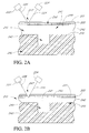
- FIGS. 2A-2C are sectional views illustrating a CMP process with enhanced light-based end point detection.
- FIGS. 3A and 3B are diagrams illustrating the reflected light intensity signal that is used in end point detection in the chemical mechanical planarization system of FIG. 1 .
- FIG. 1 is a schematic illustration which illustrates a chemical mechanical planarization (CMP) system 200 .
- the CMP system 200 incorporates a carriage 206 that is adapted to receive a wafer 210 which is to be planarized.
- the carriage 206 is rotatable about a shaft 208 in a first rotational direction, as indicated by the arrow 209 .
- This CMP system also includes a pad 201 formed of a relatively soft material, such as plastic-like polyurethane, that is adapted to be rotated about a shaft 202 in a rotational direction opposite the rotational direction of the carriage 206 as indicated by the arrows 203 .
- the CMP system 200 is also adapted so that the carriage 206 and the pad 201 can be moved relative to each other as indicated by the arrow 211 such that an exposed surface of the wafer 210 can be brought into physical contact with the pad 201 to thereby allow the pad to engage in planarization of the exposed surface of the wafer in a well-known manner.
- the system also includes a slurry supply system 207 which supplies a slurry 205 to the pad 201 .
- the slurry 205 is comprised of an etchant, abrasive particles and a suspension fluid and can be one of a large number of slurries that are particularly adapted to chemical mechanical planarization of particular materials formed on the wafer 210 .
- the pad 201 is comprised of a fixed abrasive pad having abrasives encapsulated therein and the slurry supply system 207 can be comprised of a liquid supply system that supplies a liquid to the interface between the fixed abrasive pad 201 and the wafer 210 to facilitate CMP of the wafer 210 in a well-known manner.
- the slurry supply system 207 includes a slurry or liquid reservoir 214 which provides the slurry or liquid 205 to one or more delivery tubes 204 so that the slurry or liquid can be positioned on the pad 201 .
- the slurry or liquid supply system 207 also includes a dopant supply reservoir 216 which, in this embodiment, is adapted to mix a dopant, such as a surfactant, in with the slurry or liquid 205 to enhance end point determination in a manner that will be described in greater detail below.
- a dopant such as a surfactant
- the CMP system 200 also incorporates a processor or processing system 220 that is adapted to control the CMP process performed by the system 200 .
- the processor 220 is capable of translating the pad 201 and the carriage 206 with respect to each other and then positioning the pad 201 and the carriage 206 in proximity to each other to begin the planarization process.
- the processor 220 also receives end point data from an end point detection system 221 and decides, based upon the end point data, when the end of the planarization process has occurred.
- the end point detection system 221 is comprised of one or more light sources 222 , such as a laser, that shine a beam 226 through the pad 201 onto the surface of the wafer 210 and a detector 224 that receives a reflective beam 228 from the surface of the wafer and provides a signal indicative thereof to the processor 220 .
- light sources 222 such as a laser
- the light source 222 is adapted to produce a beam 226 that is selected so that the reflective beam 228 is modulated in a detectable manner upon the planarization of the wafer 210 occurring such that a particular layer of the wafer is exposed.
- the light source 222 is comprised of a laser that produces a beam 226 of a particular wavelength that is selected so that the intensity of the reflected beam 228 increases upon the planarization of the wafer 210 occurring such that a particular layer of the wafer is exposed.
- the occurrence in the peak of intensity of the reflected beam 228 is indicative of the end point of the CMP process.
- the processor 220 Upon receiving such a signal from the detector 224 , the processor 220 is adapted to halt the CMP process.
- the system illustrated in FIG. 1 is an exemplary CMP system 200 of a type that is well known in the art.
- Examples of such a system include the MIRRA Chemical Mechanical Planarization System available from Applied Materials of Santa Clara, Calif.
- the end point detection system 221 comprised of the laser 222 and the detector 224 is similar to those types of end point detection systems that are currently available from Applied Materials of Santa Clara, Calif.
- the basic functionality of the CMP system 200 is similar to the functionality of CMP systems of the prior art.
- the CMP system 200 of the present invention is adapted to dope the liquid or slurry 205 that is being provided to the pad 201 so as to enhance end point determination.
- the end point detection system 221 comprised of the laser 222 and the detector 224 functions
- a description of an exemplary CMP process involving a shallow trench isolation structure will now be described in conjunction with FIGS. 2A-2C.
- FIG. 2A illustrates a substrate 240 having a cavity 245 formed therein.
- the substrate 240 may be comprised of any of a number of materials used in semiconductor processing, such as silicon, silicon oxide (SiO 2 ) or silicon nitride (Si 3 N 4 ).
- the substrate 240 is comprised of silicon nitride, otherwise referred to as nitride.
- the cavity 245 is formed in the nitride using well-known patterning and etching techniques. As is shown in FIG.
- an insulator material 241 such as silicon oxide (SiO 2 ) has been deposited so as to fill the cavity 245 and also so as to cover the upper surface 246 of the substrate 240 .
- the portion of the oxide 242 positioned on top of the surface 246 is simply excess oxide that is preferably removed using chemical mechanical planarization or polishing (CMP).
- CMP chemical mechanical planarization or polishing
- a pad 201 is positioned adjacent the upper surface 244 of the oxide 242 with the slurry 205 being supplied by the slurry supply system 207 so as to be interposed therebetween.
- the light source 222 is shining a beam 226 through an opening 247 in the pad 201 such that a reflected beam 228 is being received by the detector 224 .
- the reflected beam 228 in FIG. 2A is reflecting off of the slurry or liquid 205 and an exposed surface 250 of the oxide material 242 positioned on the upper surface 246 of the substrate 240 .
- the beam 226 in one embodiment, has a wavelength selected so that the intensity of the reflected beam 228 peaks when it is reflecting off of the upper surface 246 of the substrate 240 , the reflected beam 228 being received by the sensor 224 has a lower intensity when it is reflecting off of the exposed surface 250 than when the beam 228 is reflecting off of the upper surface 246 of the substrate.
- the processor 220 is adapted to look for an increase in the intensity of the reflected beam 228 resulting from the light beam 226 reflecting off the upper surface 246 of the substrate followed by a decrease as a result of scattering of the light beams 226 , 228 through the slurry or liquid 205 .
- FIG. 2B illustrates the continuation of the CMP process wherein a portion of the oxide 242 has been removed as a result of chemical mechanical planarization occurring at the surface 250 in a well-known manner.
- the processor 220 is preferably programmed such that, as the CMP process has continued for a preselected period of time, dopant from the dopant supply tank 216 is added to the slurry 205 so as to enhance end point determination.
- the dopant is comprised of a surfactant which has several effects on the slurry or liquid 205 .
- the surfactant has the effect of thinning the slurry or liquid 205 and reducing the opacity of the slurry or liquid 205 such that the light beams 226 , 228 are better able to penetrate the slurry or liquid 205 to reach and be reflected from the surface 250 that is being continuously removed by the CMP process.
- the addition of the surfactant also better disperses the abrasive particles in the slurry so that the CMP process is more uniformly applied at the surface 250 such that the tendency of particular regions of the surface 250 to polish faster than other regions is thereby reduced. This better dispersion of the particles makes it less likely that localized regions of the upper surface 246 of the substrate 240 will be exposed prior to general exposure of the upper surface 246 of the substrate 240 which reduces false indications of an end point.
- the abrasive within the slurry 205 can clump such that particular regions of the surface 250 are removed quicker than other regions of the surface 250 thereby exposing regions of the surface 246 more quickly that other regions of the surface 246 . If the light beam 226 impinges upon one of these exposed regions of the surface 246 , a higher intensity reflected beam 228 will be detected by the sensor 224 . In prior art systems, this higher intensity reflection can be viewed as an end point which would result in the termination of the CMP process before all of the oxide 242 is removed from the upper surface 246 of the wafer 210 . By adding the surfactant, the abrasive particles are more evenly distributed thereby reducing the degree of non-uniform planarization of the oxide layer 242 .
- the CMP process is continued until the beam 228 is reflecting off of the upper surface 246 of the nitride layer 240 . This results in a higher intensity beam 228 being reflected and sensed by the detector 224 .
- the end point of the CMP process can more accurately be determined which reduces the problems associated with either under-polishing or over-polishing the wafer.
- FIGS. 3A and 3B illustrate a specific embodiment of doping the slurry 205 to enhance end point detection.
- FIG. 3A is a trace of the removal of silicon oxide over a nitride substrate using a MIRRA-type CMP system having laser end point technology, such as the technology described above, wherein an oxide layer is being removed from a nitride substrate using a Corundum-type slurry available from Rodel, Inc., Delaware.
- the process represented by the trace of FIG. 3A does not include the addition of a dopant to enhance end point detection. As is demonstrated in FIG.
- the intensity of the reflected laser beam 228 received by the detector 224 indicates the existence of a plurality of false peaks 300 which can, in some circumstances, cause the processor 220 of the CMP system 200 to erroneously conclude that the end point of the CMP process has occurred.
- the Applicant believes that one explanation for this phenomenon is that this was the result of the abrasive particles within the slurry 205 being insufficiently distributed such that localized regions of the nitride surface 246 are exposed prior to general exposure of all of the nitride surface 246 .
- the CMP process creates a plurality of false peaks as the pad 201 polishes closer to the surface 246 .
- the unevenness of the removal of the layer 242 of oxide is most pronounced as the CMP process approaches the surface 246 of the nitride substrate 240 and the localized regions of the surface 246 where the oxide 242 has been removed becomes more pronounced.
- FIG. 3B is representative of a CMP process wherein a dopant solution that is a surfactant is added to the Corundum slurry during the CMP process.
- the surfactant that is added in this embodiment can be comprised of any of a number of different types of surfactants including anionic, cationic or non-ionic surfactants.
- the dopant solution is comprised of Brij 58 surfactant available from HPC Scientific, Portland, Oreg., which is a hydroxylated polyether that has a molecular weight of approximately 1000 g/mole that has been added to deionized water at approximately 3000 parts per million.
- the dopant solution is then added to a Corundum-type slurry at a ratio of approximately 8 mils of dopant solution to 100 mils of slurry.
- the dopant solution is added to the slurry 205 at a rate of 10 mils per minute while the slurry 205 is being provided to the pad 201 and wafer 210 interface at approximately 25 to 200 mils per minute during the CMP process.
- the slurry dopant mixture has approximately 275 parts per million of Brij 58, however, the Applicant has noted that in some circumstances, increasing the concentration of the surfactant in the slurry 205 to greater than 200 parts per million can affect the removal rate of the oxide 242 .
- the surfactant can be added either prior to or during the CMP process.
- the CMP process to remove approximately 1,500 too 2,000 Angstroms of oxide from a nitride substrate required approximately 3 minutes with the dopant solution being added at the onset of the CMP process.
- the Applicant believes that a dopant solution can be added at different times and still obtain desirable results.
- the Applicant believes that the dopant can be added at approximately 50% during the CMP process of the lowest typical polish time and provide end point determination enhancement.
- the exact dopant type can vary as can the time at which it is applied to the slurry 205 .
- the number of false end point peaks is significantly reduced when the dopant is added to the same CMP process that was performed and represented by FIG. 3 A.
- a single predominant intensity peak 310 occurs at the end of the CMP process and the addition of the surfactant had the effect of removing substantially all of the false peaks in the reflected intensity signal that could be falsely interpreted as an end point.
- the predominant intensity peak 310 occurs when the surface 246 is substantially exposed, as the intensity of the reflected beam 228 received by the detector 224 begins to increase.
- the end point of the CMP process can be readily determined.
- the processor 220 is programmed such that, following the peak intensity, the CMP process will be stopped after the intensity has decreased to a preselected value. This ensures that substantially all of the oxide 242 is removed from the upper surface 246 of the nitride substrate 240 leaving only the oxide material 242 filling the cavity 245 in the manner shown in FIG. 2 C.
- the processor 220 is programmed to halt the CMP process after detecting a series of intensity values which correspond to the intensity of the reflected beam 228 peaking upon the surface 246 being exposed and then decreasing as a result of the particles that are being removed from the upper surface 246 remaining in the slurry 205 , causing scattering of the beams 226 , 228 .
- doping the slurry with the surfactant significantly reduces the occurrences of false peaks that can be misinterpreted by the processor 220 as the end point of the CMP process. Consequently, the processor 220 will more accurately determine which peak corresponds to removal of the layer 242 from substantially all of the surface 246 of the substrate 240 as opposed to only localized removal of the material 242 from localized areas of the surface 246 of the substrate 240 .
- the doping of the slurry can also effectuate more accurate end point determination using any of a number of end point detection schemes.
- the adding of the dopant ensures that the abrasive within the slurry is more evenly distributed thereby reducing the tendency of localized regions of the layer to be removed by CMP at a rate faster than the removal of the layer as a whole.
- a surfactant is used as the doping characteristic and that this doping is introduced while the CMP process is occurring, any of a number of dopants that achieve more definite end point determination that are introduced either before or during the CMP process can be used without departing from the spirit of the present invention.
- the system has been described in connection with a specific application of removing an oxide layer from nitride layer, the system has a wide range of applications, including removing metals from oxides and the like.
- end point enhancement system and method described herein can be adapted for use with other types of CMP systems.
- end point enhancement process can be readily adapted to well known web-type CMP systems, including systems having stationary platens with a rotating or orbiting carrier, without departing from the spirit of the present invention.
Abstract
Description
Claims (31)
Priority Applications (2)
| Application Number | Priority Date | Filing Date | Title |
|---|---|---|---|
| US09/898,859 US6503839B2 (en) | 1999-08-11 | 2001-07-03 | Endpoint stabilization for polishing process |
| US10/285,957 US20030082867A1 (en) | 1999-08-11 | 2002-10-31 | Endpoint stabilization for polishing process |
Applications Claiming Priority (2)
| Application Number | Priority Date | Filing Date | Title |
|---|---|---|---|
| US09/371,827 US6287879B1 (en) | 1999-08-11 | 1999-08-11 | Endpoint stabilization for polishing process |
| US09/898,859 US6503839B2 (en) | 1999-08-11 | 2001-07-03 | Endpoint stabilization for polishing process |
Related Parent Applications (1)
| Application Number | Title | Priority Date | Filing Date |
|---|---|---|---|
| US09/371,827 Division US6287879B1 (en) | 1999-08-11 | 1999-08-11 | Endpoint stabilization for polishing process |
Related Child Applications (1)
| Application Number | Title | Priority Date | Filing Date |
|---|---|---|---|
| US10/285,957 Continuation US20030082867A1 (en) | 1999-08-11 | 2002-10-31 | Endpoint stabilization for polishing process |
Publications (2)
| Publication Number | Publication Date |
|---|---|
| US20020007913A1 US20020007913A1 (en) | 2002-01-24 |
| US6503839B2 true US6503839B2 (en) | 2003-01-07 |
Family
ID=23465564
Family Applications (3)
| Application Number | Title | Priority Date | Filing Date |
|---|---|---|---|
| US09/371,827 Expired - Lifetime US6287879B1 (en) | 1999-08-11 | 1999-08-11 | Endpoint stabilization for polishing process |
| US09/898,859 Expired - Lifetime US6503839B2 (en) | 1999-08-11 | 2001-07-03 | Endpoint stabilization for polishing process |
| US10/285,957 Abandoned US20030082867A1 (en) | 1999-08-11 | 2002-10-31 | Endpoint stabilization for polishing process |
Family Applications Before (1)
| Application Number | Title | Priority Date | Filing Date |
|---|---|---|---|
| US09/371,827 Expired - Lifetime US6287879B1 (en) | 1999-08-11 | 1999-08-11 | Endpoint stabilization for polishing process |
Family Applications After (1)
| Application Number | Title | Priority Date | Filing Date |
|---|---|---|---|
| US10/285,957 Abandoned US20030082867A1 (en) | 1999-08-11 | 2002-10-31 | Endpoint stabilization for polishing process |
Country Status (1)
| Country | Link |
|---|---|
| US (3) | US6287879B1 (en) |
Cited By (29)
| Publication number | Priority date | Publication date | Assignee | Title |
|---|---|---|---|---|
| US20020103866A1 (en) * | 2000-11-30 | 2002-08-01 | Chi Yueh-Shian T. | Dynamic subject information generation in message services of distributed object systems |
| US20020128735A1 (en) * | 2001-03-08 | 2002-09-12 | Hawkins Parris C.M. | Dynamic and extensible task guide |
| US20020138321A1 (en) * | 2001-03-20 | 2002-09-26 | Applied Materials, Inc. | Fault tolerant and automated computer software workflow |
| US20020156548A1 (en) * | 1999-07-29 | 2002-10-24 | Applied Materials, Inc. | Computer integrated manufacturing techniques |
| US20020197745A1 (en) * | 2001-06-19 | 2002-12-26 | Shanmugasundram Arulkumar P. | Feedback control of a chemical mechanical polishing device providing manipulation of removal rate profiles |
| US20030027424A1 (en) * | 2001-06-19 | 2003-02-06 | Paik Young Joseph | Feedforward and feedback control for conditioning of chemical mechanical polishing pad |
| US20030049376A1 (en) * | 2001-06-19 | 2003-03-13 | Applied Materials, Inc. | Feedback control of sub-atmospheric chemical vapor deposition processes |
| US20030049390A1 (en) * | 2001-06-19 | 2003-03-13 | Applied Materials, Inc. | Feedback control of plasma-enhanced chemical vapor deposition processes |
| US20030180972A1 (en) * | 2002-03-19 | 2003-09-25 | Amir Al-Bayati | Method, system and medium for controlling semiconductor wafer processes using critical dimension measurements |
| US20030199112A1 (en) * | 2002-03-22 | 2003-10-23 | Applied Materials, Inc. | Copper wiring module control |
| US6638140B2 (en) * | 2000-09-22 | 2003-10-28 | Sony Corporation | Method and apparatus for polishing |
| US6640151B1 (en) | 1999-12-22 | 2003-10-28 | Applied Materials, Inc. | Multi-tool control system, method and medium |
| US20030202070A1 (en) * | 2002-04-29 | 2003-10-30 | Xerox Corporation | Multiple portion solid ink stick |
| US6708074B1 (en) | 2000-08-11 | 2004-03-16 | Applied Materials, Inc. | Generic interface builder |
| US20040148049A1 (en) * | 2003-01-21 | 2004-07-29 | Applied Materials, Inc. | Automated design and execution of experiments with integrated model creation for semiconductor manufacturing tools |
| US20040248409A1 (en) * | 2003-06-03 | 2004-12-09 | Applied Materials, Inc. | Selective metal encapsulation schemes |
| US20050014299A1 (en) * | 2003-07-15 | 2005-01-20 | Applied Materials, Inc. | Control of metal resistance in semiconductor products via integrated metrology |
| US20050032459A1 (en) * | 2003-08-04 | 2005-02-10 | Applied Materials, Inc. | Technique for process-qualifying a semiconductor manufacturing tool using metrology data |
| US20050170640A1 (en) * | 2002-12-10 | 2005-08-04 | Fujitsu Limited | Semiconductor device, wiring substrate forming method, and substrate processing apparatus |
| US20050171626A1 (en) * | 2004-01-29 | 2005-08-04 | Applied Materials, Inc. | System, method, and medium for monitoring performance of an advanced process control system |
| US6939198B1 (en) | 2001-12-28 | 2005-09-06 | Applied Materials, Inc. | Polishing system with in-line and in-situ metrology |
| US20050267607A1 (en) * | 2004-05-28 | 2005-12-01 | Applied Materials, Inc. | Dynamic offset and feedback threshold |
| US20050278051A1 (en) * | 2004-05-28 | 2005-12-15 | Applied Materials, Inc. | Process control by distinguishing a white noise component of a process variance |
| US20060079007A1 (en) * | 2004-10-08 | 2006-04-13 | Applied Materials, Inc. | System, method, and medium for an endpoint detection scheme for copper low-dielectric damascene structures for improved dielectric and copper loss |
| US20080021571A1 (en) * | 2002-11-15 | 2008-01-24 | Yuri Kokotov | Method, system and medium for controlling manufacture process having multivariate input parameters |
| US20080109089A1 (en) * | 2001-06-19 | 2008-05-08 | Shanmugasundram Arulkumar P | Dynamic metrology schemes and sampling schemes for advanced process control in semiconductor processing |
| US20080124896A1 (en) * | 2006-11-28 | 2008-05-29 | International Business Machines Corporation | Silicon wafer thinning end point method |
| US11282755B2 (en) | 2019-08-27 | 2022-03-22 | Applied Materials, Inc. | Asymmetry correction via oriented wafer loading |
| US11291502B2 (en) | 2012-11-05 | 2022-04-05 | Relievant Medsystems, Inc. | Methods of navigation and treatment within a vertebral body |
Families Citing this family (27)
| Publication number | Priority date | Publication date | Assignee | Title |
|---|---|---|---|---|
| US6075606A (en) | 1996-02-16 | 2000-06-13 | Doan; Trung T. | Endpoint detector and method for measuring a change in wafer thickness in chemical-mechanical polishing of semiconductor wafers and other microelectronic substrates |
| US6395563B1 (en) | 1998-12-28 | 2002-05-28 | Matsushita Electric Industrial Co., Ltd. | Device for manufacturing semiconductor device and method of manufacturing the same |
| US6628397B1 (en) * | 1999-09-15 | 2003-09-30 | Kla-Tencor | Apparatus and methods for performing self-clearing optical measurements |
| US6671051B1 (en) * | 1999-09-15 | 2003-12-30 | Kla-Tencor | Apparatus and methods for detecting killer particles during chemical mechanical polishing |
| US6498101B1 (en) | 2000-02-28 | 2002-12-24 | Micron Technology, Inc. | Planarizing pads, planarizing machines and methods for making and using planarizing pads in mechanical and chemical-mechanical planarization of microelectronic device substrate assemblies |
| DE10010820C1 (en) * | 2000-02-29 | 2001-09-13 | Infineon Technologies Ag | Process for the regeneration of semiconductor wafers |
| US6313038B1 (en) | 2000-04-26 | 2001-11-06 | Micron Technology, Inc. | Method and apparatus for controlling chemical interactions during planarization of microelectronic substrates |
| US6387289B1 (en) | 2000-05-04 | 2002-05-14 | Micron Technology, Inc. | Planarizing machines and methods for mechanical and/or chemical-mechanical planarization of microelectronic-device substrate assemblies |
| US6612901B1 (en) | 2000-06-07 | 2003-09-02 | Micron Technology, Inc. | Apparatus for in-situ optical endpointing of web-format planarizing machines in mechanical or chemical-mechanical planarization of microelectronic-device substrate assemblies |
| US6520834B1 (en) | 2000-08-09 | 2003-02-18 | Micron Technology, Inc. | Methods and apparatuses for analyzing and controlling performance parameters in mechanical and chemical-mechanical planarization of microelectronic substrates |
| US6736869B1 (en) | 2000-08-28 | 2004-05-18 | Micron Technology, Inc. | Method for forming a planarizing pad for planarization of microelectronic substrates |
| US6592443B1 (en) | 2000-08-30 | 2003-07-15 | Micron Technology, Inc. | Method and apparatus for forming and using planarizing pads for mechanical and chemical-mechanical planarization of microelectronic substrates |
| US6623329B1 (en) | 2000-08-31 | 2003-09-23 | Micron Technology, Inc. | Method and apparatus for supporting a microelectronic substrate relative to a planarization pad |
| US6652764B1 (en) | 2000-08-31 | 2003-11-25 | Micron Technology, Inc. | Methods and apparatuses for making and using planarizing pads for mechanical and chemical-mechanical planarization of microelectronic substrates |
| US6336841B1 (en) * | 2001-03-29 | 2002-01-08 | Macronix International Co. Ltd. | Method of CMP endpoint detection |
| US6514775B2 (en) * | 2001-06-29 | 2003-02-04 | Kla-Tencor Technologies Corporation | In-situ end point detection for semiconductor wafer polishing |
| US6666749B2 (en) | 2001-08-30 | 2003-12-23 | Micron Technology, Inc. | Apparatus and method for enhanced processing of microelectronic workpieces |
| US6509249B1 (en) * | 2002-05-28 | 2003-01-21 | Macronix International Co., Ltd. | Method of fabricating shallow trench isolation |
| US6653202B1 (en) * | 2003-01-17 | 2003-11-25 | Advanced Micro Devices, Inc. | Method of shallow trench isolation (STI) formation using amorphous carbon |
| ATE552934T1 (en) * | 2003-06-06 | 2012-04-15 | Electro Scient Ind Inc | LASER PROCESSING USING A SURFACTANT FILM |
| US6939211B2 (en) * | 2003-10-09 | 2005-09-06 | Micron Technology, Inc. | Planarizing solutions including abrasive elements, and methods for manufacturing and using such planarizing solutions |
| US7361601B2 (en) * | 2005-06-21 | 2008-04-22 | Macronix International Co., Ltd. | Chemical mechanical polish process and method for improving accuracy of determining polish endpoint thereof |
| US20070032808A1 (en) * | 2005-08-03 | 2007-02-08 | Azam Anwar | System and method for addressing total occlusion in a vascular environment |
| IL194029A (en) * | 2008-09-11 | 2013-11-28 | Israel Aerospace Ind Ltd | System and method for identification of a distant seaborne object |
| WO2014070172A1 (en) * | 2012-10-31 | 2014-05-08 | Duescher Wayne O | Abrasive platen wafer surface optical monitoring system |
| US9443763B2 (en) * | 2013-09-12 | 2016-09-13 | Micron Technology, Inc. | Methods for forming interconnections between top electrodes in memory cells by a two-step chemical-mechanical polishing (CMP) process |
| US10875149B2 (en) * | 2017-03-30 | 2020-12-29 | Taiwan Semiconductor Manufacturing Co., Ltd. | Apparatus and method for timed dispensing various slurry components |
Citations (21)
| Publication number | Priority date | Publication date | Assignee | Title |
|---|---|---|---|---|
| US5225034A (en) | 1992-06-04 | 1993-07-06 | Micron Technology, Inc. | Method of chemical mechanical polishing predominantly copper containing metal layers in semiconductor processing |
| US5234540A (en) | 1992-04-30 | 1993-08-10 | Submicron Systems, Inc. | Process for etching oxide films in a sealed photochemical reactor |
| US5240522A (en) | 1991-03-29 | 1993-08-31 | Sumitomo Light Metal Industries, Ltd. | Method of producing hardened aluminum alloy sheets having superior thermal stability |
| US5242524A (en) | 1990-05-16 | 1993-09-07 | International Business Machines Corporation | Device for detecting an end point in polishing operations |
| US5314843A (en) | 1992-03-27 | 1994-05-24 | Micron Technology, Inc. | Integrated circuit polishing method |
| US5376483A (en) | 1993-10-07 | 1994-12-27 | Micron Semiconductor, Inc. | Method of making masks for phase shifting lithography |
| US5407526A (en) | 1993-06-30 | 1995-04-18 | Intel Corporation | Chemical mechanical polishing slurry delivery and mixing system |
| US5413941A (en) | 1994-01-06 | 1995-05-09 | Micron Technology, Inc. | Optical end point detection methods in semiconductor planarizing polishing processes |
| US5439553A (en) | 1994-03-30 | 1995-08-08 | Penn State Research Foundation | Controlled etching of oxides via gas phase reactions |
| US5576126A (en) | 1994-09-26 | 1996-11-19 | Micron Technology, Inc. | Phase shifting mask |
| US5637185A (en) | 1995-03-30 | 1997-06-10 | Rensselaer Polytechnic Institute | Systems for performing chemical mechanical planarization and process for conducting same |
| US5667424A (en) * | 1996-09-25 | 1997-09-16 | Chartered Semiconductor Manufacturing Pte Ltd. | New chemical mechanical planarization (CMP) end point detection apparatus |
| US5685951A (en) | 1996-02-15 | 1997-11-11 | Micron Technology, Inc. | Methods and etchants for etching oxides of silicon with low selectivity in a vapor phase system |
| US5783495A (en) | 1995-11-13 | 1998-07-21 | Micron Technology, Inc. | Method of wafer cleaning, and system and cleaning solution regarding same |
| US6022807A (en) | 1996-04-24 | 2000-02-08 | Micro Processing Technology, Inc. | Method for fabricating an integrated circuit |
| US6099604A (en) * | 1997-08-21 | 2000-08-08 | Micron Technology, Inc. | Slurry with chelating agent for chemical-mechanical polishing of a semiconductor wafer and methods related thereto |
| US6117783A (en) | 1996-07-25 | 2000-09-12 | Ekc Technology, Inc. | Chemical mechanical polishing composition and process |
| US6214732B1 (en) * | 1999-11-01 | 2001-04-10 | Lucent Technologies, Inc. | Chemical mechanical polishing endpoint detection by monitoring component activity in effluent slurry |
| US6238270B1 (en) * | 1996-05-21 | 2001-05-29 | Micron Technology, Inc. | Method for conditioning a polishing pad used in chemical-mechanical planarization of semiconductor wafers |
| US6261851B1 (en) * | 1999-09-30 | 2001-07-17 | International Business Machines Corporation | Optimization of CMP process by detecting of oxide/nitride interface using IR system |
| US6303507B1 (en) * | 1999-12-13 | 2001-10-16 | Advanced Micro Devices, Inc. | In-situ feedback system for localized CMP thickness control |
-
1999
- 1999-08-11 US US09/371,827 patent/US6287879B1/en not_active Expired - Lifetime
-
2001
- 2001-07-03 US US09/898,859 patent/US6503839B2/en not_active Expired - Lifetime
-
2002
- 2002-10-31 US US10/285,957 patent/US20030082867A1/en not_active Abandoned
Patent Citations (21)
| Publication number | Priority date | Publication date | Assignee | Title |
|---|---|---|---|---|
| US5242524A (en) | 1990-05-16 | 1993-09-07 | International Business Machines Corporation | Device for detecting an end point in polishing operations |
| US5240522A (en) | 1991-03-29 | 1993-08-31 | Sumitomo Light Metal Industries, Ltd. | Method of producing hardened aluminum alloy sheets having superior thermal stability |
| US5314843A (en) | 1992-03-27 | 1994-05-24 | Micron Technology, Inc. | Integrated circuit polishing method |
| US5234540A (en) | 1992-04-30 | 1993-08-10 | Submicron Systems, Inc. | Process for etching oxide films in a sealed photochemical reactor |
| US5225034A (en) | 1992-06-04 | 1993-07-06 | Micron Technology, Inc. | Method of chemical mechanical polishing predominantly copper containing metal layers in semiconductor processing |
| US5407526A (en) | 1993-06-30 | 1995-04-18 | Intel Corporation | Chemical mechanical polishing slurry delivery and mixing system |
| US5376483A (en) | 1993-10-07 | 1994-12-27 | Micron Semiconductor, Inc. | Method of making masks for phase shifting lithography |
| US5413941A (en) | 1994-01-06 | 1995-05-09 | Micron Technology, Inc. | Optical end point detection methods in semiconductor planarizing polishing processes |
| US5439553A (en) | 1994-03-30 | 1995-08-08 | Penn State Research Foundation | Controlled etching of oxides via gas phase reactions |
| US5576126A (en) | 1994-09-26 | 1996-11-19 | Micron Technology, Inc. | Phase shifting mask |
| US5637185A (en) | 1995-03-30 | 1997-06-10 | Rensselaer Polytechnic Institute | Systems for performing chemical mechanical planarization and process for conducting same |
| US5783495A (en) | 1995-11-13 | 1998-07-21 | Micron Technology, Inc. | Method of wafer cleaning, and system and cleaning solution regarding same |
| US5685951A (en) | 1996-02-15 | 1997-11-11 | Micron Technology, Inc. | Methods and etchants for etching oxides of silicon with low selectivity in a vapor phase system |
| US6022807A (en) | 1996-04-24 | 2000-02-08 | Micro Processing Technology, Inc. | Method for fabricating an integrated circuit |
| US6238270B1 (en) * | 1996-05-21 | 2001-05-29 | Micron Technology, Inc. | Method for conditioning a polishing pad used in chemical-mechanical planarization of semiconductor wafers |
| US6117783A (en) | 1996-07-25 | 2000-09-12 | Ekc Technology, Inc. | Chemical mechanical polishing composition and process |
| US5667424A (en) * | 1996-09-25 | 1997-09-16 | Chartered Semiconductor Manufacturing Pte Ltd. | New chemical mechanical planarization (CMP) end point detection apparatus |
| US6099604A (en) * | 1997-08-21 | 2000-08-08 | Micron Technology, Inc. | Slurry with chelating agent for chemical-mechanical polishing of a semiconductor wafer and methods related thereto |
| US6261851B1 (en) * | 1999-09-30 | 2001-07-17 | International Business Machines Corporation | Optimization of CMP process by detecting of oxide/nitride interface using IR system |
| US6214732B1 (en) * | 1999-11-01 | 2001-04-10 | Lucent Technologies, Inc. | Chemical mechanical polishing endpoint detection by monitoring component activity in effluent slurry |
| US6303507B1 (en) * | 1999-12-13 | 2001-10-16 | Advanced Micro Devices, Inc. | In-situ feedback system for localized CMP thickness control |
Non-Patent Citations (1)
| Title |
|---|
| Kojima et al., "Application of CMP Process Monitor to Cu Polishing", 2000 IEEE, pp. 293-298, Aug. 2000. |
Cited By (58)
| Publication number | Priority date | Publication date | Assignee | Title |
|---|---|---|---|---|
| US20020156548A1 (en) * | 1999-07-29 | 2002-10-24 | Applied Materials, Inc. | Computer integrated manufacturing techniques |
| US20040083021A1 (en) * | 1999-12-22 | 2004-04-29 | Applied Materials, Inc. | Multi-tool control system, method and medium |
| US6640151B1 (en) | 1999-12-22 | 2003-10-28 | Applied Materials, Inc. | Multi-tool control system, method and medium |
| US6708074B1 (en) | 2000-08-11 | 2004-03-16 | Applied Materials, Inc. | Generic interface builder |
| US6638140B2 (en) * | 2000-09-22 | 2003-10-28 | Sony Corporation | Method and apparatus for polishing |
| US20020103866A1 (en) * | 2000-11-30 | 2002-08-01 | Chi Yueh-Shian T. | Dynamic subject information generation in message services of distributed object systems |
| US20070112928A1 (en) * | 2000-11-30 | 2007-05-17 | Applied Materials, Inc. | Dynamic subject information generation in message services of distributed object systems |
| US8504620B2 (en) | 2000-11-30 | 2013-08-06 | Applied Materials, Inc. | Dynamic subject information generation in message services of distributed object systems |
| US20020128735A1 (en) * | 2001-03-08 | 2002-09-12 | Hawkins Parris C.M. | Dynamic and extensible task guide |
| US20020138321A1 (en) * | 2001-03-20 | 2002-09-26 | Applied Materials, Inc. | Fault tolerant and automated computer software workflow |
| US20030027424A1 (en) * | 2001-06-19 | 2003-02-06 | Paik Young Joseph | Feedforward and feedback control for conditioning of chemical mechanical polishing pad |
| US8694145B2 (en) | 2001-06-19 | 2014-04-08 | Applied Materials, Inc. | Feedback control of a chemical mechanical polishing device providing manipulation of removal rate profiles |
| US8070909B2 (en) | 2001-06-19 | 2011-12-06 | Applied Materials, Inc. | Feedback control of chemical mechanical polishing device providing manipulation of removal rate profiles |
| US20030049390A1 (en) * | 2001-06-19 | 2003-03-13 | Applied Materials, Inc. | Feedback control of plasma-enhanced chemical vapor deposition processes |
| US20030049376A1 (en) * | 2001-06-19 | 2003-03-13 | Applied Materials, Inc. | Feedback control of sub-atmospheric chemical vapor deposition processes |
| US7783375B2 (en) | 2001-06-19 | 2010-08-24 | Applied Materials, Inc. | Dynamic metrology schemes and sampling schemes for advanced process control in semiconductor processing |
| US7725208B2 (en) | 2001-06-19 | 2010-05-25 | Applied Materials, Inc. | Dynamic metrology schemes and sampling schemes for advanced process control in semiconductor processing |
| US7698012B2 (en) | 2001-06-19 | 2010-04-13 | Applied Materials, Inc. | Dynamic metrology schemes and sampling schemes for advanced process control in semiconductor processing |
| US20080109089A1 (en) * | 2001-06-19 | 2008-05-08 | Shanmugasundram Arulkumar P | Dynamic metrology schemes and sampling schemes for advanced process control in semiconductor processing |
| US20070169694A1 (en) * | 2001-06-19 | 2007-07-26 | Applied Materials, Inc. | Feedback control of sub-atmospheric chemical vapor deposition processes |
| US20060009129A1 (en) * | 2001-06-19 | 2006-01-12 | Applied Materials, Inc. | Feedforward and feedback control for conditioning of chemical mechanical polishing pad |
| US20070102116A1 (en) * | 2001-06-19 | 2007-05-10 | Applied Materials, Inc. | Feedback control of chemical mechanical polishing device providing manipulation of removal rate profiles |
| US20020197745A1 (en) * | 2001-06-19 | 2002-12-26 | Shanmugasundram Arulkumar P. | Feedback control of a chemical mechanical polishing device providing manipulation of removal rate profiles |
| US20060286904A1 (en) * | 2001-12-28 | 2006-12-21 | Applied Materials, Inc. | Polishing System With In-Line and In-Situ Metrology |
| US6939198B1 (en) | 2001-12-28 | 2005-09-06 | Applied Materials, Inc. | Polishing system with in-line and in-situ metrology |
| US20100062684A1 (en) * | 2001-12-28 | 2010-03-11 | Applied Materials, Inc. | Polishing system with in-line and in-situ metrology |
| US7927182B2 (en) | 2001-12-28 | 2011-04-19 | Applied Materials, Inc. | Polishing system with in-line and in-situ metrology |
| US8460057B2 (en) | 2001-12-28 | 2013-06-11 | Applied Materials, Inc. | Computer-implemented process control in chemical mechanical polishing |
| US7101251B2 (en) | 2001-12-28 | 2006-09-05 | Applied Materials, Inc. | Polishing system with in-line and in-situ metrology |
| US20050245170A1 (en) * | 2001-12-28 | 2005-11-03 | Applied Materials, Inc., A Delaware Corporation | Polishing system with in-line and in-situ metrology |
| US7585202B2 (en) | 2001-12-28 | 2009-09-08 | Applied Materials, Inc. | Computer-implemented method for process control in chemical mechanical polishing |
| US20110195528A1 (en) * | 2001-12-28 | 2011-08-11 | Swedek Boguslaw A | Polishing system with in-line and in-situ metrology |
| US7294039B2 (en) | 2001-12-28 | 2007-11-13 | Applied Materials, Inc. | Polishing system with in-line and in-situ metrology |
| US20030180972A1 (en) * | 2002-03-19 | 2003-09-25 | Amir Al-Bayati | Method, system and medium for controlling semiconductor wafer processes using critical dimension measurements |
| US8005634B2 (en) | 2002-03-22 | 2011-08-23 | Applied Materials, Inc. | Copper wiring module control |
| US20070122921A1 (en) * | 2002-03-22 | 2007-05-31 | Applied Materials, Inc. | Copper Wiring Module Control |
| US20030199112A1 (en) * | 2002-03-22 | 2003-10-23 | Applied Materials, Inc. | Copper wiring module control |
| US20030202070A1 (en) * | 2002-04-29 | 2003-10-30 | Xerox Corporation | Multiple portion solid ink stick |
| US7966087B2 (en) | 2002-11-15 | 2011-06-21 | Applied Materials, Inc. | Method, system and medium for controlling manufacture process having multivariate input parameters |
| US20080021571A1 (en) * | 2002-11-15 | 2008-01-24 | Yuri Kokotov | Method, system and medium for controlling manufacture process having multivariate input parameters |
| US20050170640A1 (en) * | 2002-12-10 | 2005-08-04 | Fujitsu Limited | Semiconductor device, wiring substrate forming method, and substrate processing apparatus |
| US7485962B2 (en) * | 2002-12-10 | 2009-02-03 | Fujitsu Limited | Semiconductor device, wiring substrate forming method, and substrate processing apparatus |
| US20040148049A1 (en) * | 2003-01-21 | 2004-07-29 | Applied Materials, Inc. | Automated design and execution of experiments with integrated model creation for semiconductor manufacturing tools |
| US20040248409A1 (en) * | 2003-06-03 | 2004-12-09 | Applied Materials, Inc. | Selective metal encapsulation schemes |
| US20050014299A1 (en) * | 2003-07-15 | 2005-01-20 | Applied Materials, Inc. | Control of metal resistance in semiconductor products via integrated metrology |
| US20050032459A1 (en) * | 2003-08-04 | 2005-02-10 | Applied Materials, Inc. | Technique for process-qualifying a semiconductor manufacturing tool using metrology data |
| US20050171626A1 (en) * | 2004-01-29 | 2005-08-04 | Applied Materials, Inc. | System, method, and medium for monitoring performance of an advanced process control system |
| US20050278051A1 (en) * | 2004-05-28 | 2005-12-15 | Applied Materials, Inc. | Process control by distinguishing a white noise component of a process variance |
| US20060195214A1 (en) * | 2004-05-28 | 2006-08-31 | Applied Materials, Inc. | Process control by distinguishing a white noise component of a process variance |
| US20050267607A1 (en) * | 2004-05-28 | 2005-12-01 | Applied Materials, Inc. | Dynamic offset and feedback threshold |
| US7848839B2 (en) | 2004-10-08 | 2010-12-07 | Applied Materials, Inc. | System, method, and medium for an endpoint detection scheme for copper low-dielectric damascene structures for improved dielectric and copper loss |
| US20080109104A1 (en) * | 2004-10-08 | 2008-05-08 | Ajoy Zutshi | System, method, and medium for an endpoint detection scheme for copper low-dielectric damascene structures for improved dielectric and copper loss |
| US20060079007A1 (en) * | 2004-10-08 | 2006-04-13 | Applied Materials, Inc. | System, method, and medium for an endpoint detection scheme for copper low-dielectric damascene structures for improved dielectric and copper loss |
| US20080124896A1 (en) * | 2006-11-28 | 2008-05-29 | International Business Machines Corporation | Silicon wafer thinning end point method |
| US7498236B2 (en) | 2006-11-28 | 2009-03-03 | International Business Machines Corporation | Silicon wafer thinning end point method |
| US11291502B2 (en) | 2012-11-05 | 2022-04-05 | Relievant Medsystems, Inc. | Methods of navigation and treatment within a vertebral body |
| US11282755B2 (en) | 2019-08-27 | 2022-03-22 | Applied Materials, Inc. | Asymmetry correction via oriented wafer loading |
| US11869815B2 (en) | 2019-08-27 | 2024-01-09 | Applied Materials, Inc. | Asymmetry correction via oriented wafer loading |
Also Published As
| Publication number | Publication date |
|---|---|
| US20030082867A1 (en) | 2003-05-01 |
| US20020007913A1 (en) | 2002-01-24 |
| US6287879B1 (en) | 2001-09-11 |
Similar Documents
| Publication | Publication Date | Title |
|---|---|---|
| US6503839B2 (en) | Endpoint stabilization for polishing process | |
| US7132035B2 (en) | Methods, apparatuses, and substrate assembly structures for fabricating microelectronic components using mechanical and chemical-mechanical planarization processes | |
| US6276997B1 (en) | Use of chemical mechanical polishing and/or poly-vinyl-acetate scrubbing to restore quality of used semiconductor wafers | |
| US4879258A (en) | Integrated circuit planarization by mechanical polishing | |
| US6423640B1 (en) | Headless CMP process for oxide planarization | |
| Landis et al. | Integration of chemical-mechanical polishing into CMOS integrated circuit manufacturing | |
| US5913712A (en) | Scratch reduction in semiconductor circuit fabrication using chemical-mechanical polishing | |
| US6046111A (en) | Method and apparatus for endpointing mechanical and chemical-mechanical planarization of microelectronic substrates | |
| JP3004891B2 (en) | Rough polishing method for semiconductor wafers to reduce surface roughness | |
| US5449314A (en) | Method of chimical mechanical polishing for dielectric layers | |
| US7101251B2 (en) | Polishing system with in-line and in-situ metrology | |
| US6071177A (en) | Method and apparatus for determining end point in a polishing process | |
| US6426288B1 (en) | Method for removing an upper layer of material from a semiconductor wafer | |
| EP1295322B1 (en) | Two steps chemical mechanical polishing process | |
| US5830041A (en) | Method and apparatus for determining endpoint during a polishing process | |
| KR20000058021A (en) | Chemical mechanical polishing processes and components | |
| US6069081A (en) | Two-step chemical mechanical polish surface planarization technique | |
| US6380092B1 (en) | Gas phase planarization process for semiconductor wafers | |
| US6165052A (en) | Method and apparatus for chemical/mechanical planarization (CMP) of a semiconductor substrate having shallow trench isolation | |
| US8129278B2 (en) | Chemical mechanical polishing process | |
| EP0808231B1 (en) | Chemical-mechanical polishing using curved carriers | |
| US6609946B1 (en) | Method and system for polishing a semiconductor wafer | |
| US6189546B1 (en) | Polishing process for manufacturing dopant-striation-free polished silicon wafers | |
| US6403385B1 (en) | Method of inspecting a semiconductor wafer for defects | |
| WO1996027206A2 (en) | Polysilicon polish for patterning improvement |
Legal Events
| Date | Code | Title | Description |
|---|---|---|---|
| AS | Assignment |
Owner name: MICRON TECHNOLOGY, INC., IDAHO Free format text: ASSIGNMENT OF ASSIGNORS INTEREST;ASSIGNORS:GONZALES, DAVID B.;BARTLETT, AARON T.;REEL/FRAME:012253/0483 Effective date: 19990804 |
|
| STCF | Information on status: patent grant |
Free format text: PATENTED CASE |
|
| FEPP | Fee payment procedure |
Free format text: PAYOR NUMBER ASSIGNED (ORIGINAL EVENT CODE: ASPN); ENTITY STATUS OF PATENT OWNER: LARGE ENTITY |
|
| FPAY | Fee payment |
Year of fee payment: 4 |
|
| FPAY | Fee payment |
Year of fee payment: 8 |
|
| FPAY | Fee payment |
Year of fee payment: 12 |
|
| AS | Assignment |
Owner name: U.S. BANK NATIONAL ASSOCIATION, AS COLLATERAL AGENT, CALIFORNIA Free format text: SECURITY INTEREST;ASSIGNOR:MICRON TECHNOLOGY, INC.;REEL/FRAME:038669/0001 Effective date: 20160426 Owner name: U.S. BANK NATIONAL ASSOCIATION, AS COLLATERAL AGEN Free format text: SECURITY INTEREST;ASSIGNOR:MICRON TECHNOLOGY, INC.;REEL/FRAME:038669/0001 Effective date: 20160426 |
|
| AS | Assignment |
Owner name: MORGAN STANLEY SENIOR FUNDING, INC., AS COLLATERAL AGENT, MARYLAND Free format text: PATENT SECURITY AGREEMENT;ASSIGNOR:MICRON TECHNOLOGY, INC.;REEL/FRAME:038954/0001 Effective date: 20160426 Owner name: MORGAN STANLEY SENIOR FUNDING, INC., AS COLLATERAL Free format text: PATENT SECURITY AGREEMENT;ASSIGNOR:MICRON TECHNOLOGY, INC.;REEL/FRAME:038954/0001 Effective date: 20160426 |
|
| AS | Assignment |
Owner name: U.S. BANK NATIONAL ASSOCIATION, AS COLLATERAL AGENT, CALIFORNIA Free format text: CORRECTIVE ASSIGNMENT TO CORRECT THE REPLACE ERRONEOUSLY FILED PATENT #7358718 WITH THE CORRECT PATENT #7358178 PREVIOUSLY RECORDED ON REEL 038669 FRAME 0001. ASSIGNOR(S) HEREBY CONFIRMS THE SECURITY INTEREST;ASSIGNOR:MICRON TECHNOLOGY, INC.;REEL/FRAME:043079/0001 Effective date: 20160426 Owner name: U.S. BANK NATIONAL ASSOCIATION, AS COLLATERAL AGEN Free format text: CORRECTIVE ASSIGNMENT TO CORRECT THE REPLACE ERRONEOUSLY FILED PATENT #7358718 WITH THE CORRECT PATENT #7358178 PREVIOUSLY RECORDED ON REEL 038669 FRAME 0001. ASSIGNOR(S) HEREBY CONFIRMS THE SECURITY INTEREST;ASSIGNOR:MICRON TECHNOLOGY, INC.;REEL/FRAME:043079/0001 Effective date: 20160426 |
|
| AS | Assignment |
Owner name: JPMORGAN CHASE BANK, N.A., AS COLLATERAL AGENT, ILLINOIS Free format text: SECURITY INTEREST;ASSIGNORS:MICRON TECHNOLOGY, INC.;MICRON SEMICONDUCTOR PRODUCTS, INC.;REEL/FRAME:047540/0001 Effective date: 20180703 Owner name: JPMORGAN CHASE BANK, N.A., AS COLLATERAL AGENT, IL Free format text: SECURITY INTEREST;ASSIGNORS:MICRON TECHNOLOGY, INC.;MICRON SEMICONDUCTOR PRODUCTS, INC.;REEL/FRAME:047540/0001 Effective date: 20180703 |
|
| AS | Assignment |
Owner name: MICRON TECHNOLOGY, INC., IDAHO Free format text: RELEASE BY SECURED PARTY;ASSIGNOR:U.S. BANK NATIONAL ASSOCIATION, AS COLLATERAL AGENT;REEL/FRAME:047243/0001 Effective date: 20180629 |
|
| AS | Assignment |
Owner name: MICRON TECHNOLOGY, INC., IDAHO Free format text: RELEASE BY SECURED PARTY;ASSIGNOR:MORGAN STANLEY SENIOR FUNDING, INC., AS COLLATERAL AGENT;REEL/FRAME:050937/0001 Effective date: 20190731 |
|
| AS | Assignment |
Owner name: MICRON SEMICONDUCTOR PRODUCTS, INC., IDAHO Free format text: RELEASE BY SECURED PARTY;ASSIGNOR:JPMORGAN CHASE BANK, N.A., AS COLLATERAL AGENT;REEL/FRAME:051028/0001 Effective date: 20190731 Owner name: MICRON TECHNOLOGY, INC., IDAHO Free format text: RELEASE BY SECURED PARTY;ASSIGNOR:JPMORGAN CHASE BANK, N.A., AS COLLATERAL AGENT;REEL/FRAME:051028/0001 Effective date: 20190731 |