US6503768B2 - Method for monolithic integration of multiple devices on an optoelectronic substrate - Google Patents
Method for monolithic integration of multiple devices on an optoelectronic substrate Download PDFInfo
- Publication number
- US6503768B2 US6503768B2 US09/821,212 US82121201A US6503768B2 US 6503768 B2 US6503768 B2 US 6503768B2 US 82121201 A US82121201 A US 82121201A US 6503768 B2 US6503768 B2 US 6503768B2
- Authority
- US
- United States
- Prior art keywords
- given wavelength
- active region
- recited
- layer
- altering
- Prior art date
- Legal status (The legal status is an assumption and is not a legal conclusion. Google has not performed a legal analysis and makes no representation as to the accuracy of the status listed.)
- Expired - Lifetime
Links
Images


Classifications
-
- H—ELECTRICITY
- H01—ELECTRIC ELEMENTS
- H01S—DEVICES USING THE PROCESS OF LIGHT AMPLIFICATION BY STIMULATED EMISSION OF RADIATION [LASER] TO AMPLIFY OR GENERATE LIGHT; DEVICES USING STIMULATED EMISSION OF ELECTROMAGNETIC RADIATION IN WAVE RANGES OTHER THAN OPTICAL
- H01S5/00—Semiconductor lasers
- H01S5/02—Structural details or components not essential to laser action
- H01S5/026—Monolithically integrated components, e.g. waveguides, monitoring photo-detectors, drivers
- H01S5/0265—Intensity modulators
-
- H—ELECTRICITY
- H01—ELECTRIC ELEMENTS
- H01S—DEVICES USING THE PROCESS OF LIGHT AMPLIFICATION BY STIMULATED EMISSION OF RADIATION [LASER] TO AMPLIFY OR GENERATE LIGHT; DEVICES USING STIMULATED EMISSION OF ELECTROMAGNETIC RADIATION IN WAVE RANGES OTHER THAN OPTICAL
- H01S5/00—Semiconductor lasers
- H01S5/40—Arrangement of two or more semiconductor lasers, not provided for in groups H01S5/02 - H01S5/30
- H01S5/4025—Array arrangements, e.g. constituted by discrete laser diodes or laser bar
- H01S5/4031—Edge-emitting structures
-
- H—ELECTRICITY
- H01—ELECTRIC ELEMENTS
- H01S—DEVICES USING THE PROCESS OF LIGHT AMPLIFICATION BY STIMULATED EMISSION OF RADIATION [LASER] TO AMPLIFY OR GENERATE LIGHT; DEVICES USING STIMULATED EMISSION OF ELECTROMAGNETIC RADIATION IN WAVE RANGES OTHER THAN OPTICAL
- H01S5/00—Semiconductor lasers
- H01S5/50—Amplifier structures not provided for in groups H01S5/02 - H01S5/30
Definitions
- the present invention is directed, in general, to telecommunication systems and, more specifically, to a method for monolithic integration of multiple devices on an optoelectronic substrate, and a method of manufacturing an optical fiber communications system associated therewith.
- Optical fibers are key components in modern telecommunications and have gained wide acceptance.
- telecommunication optical fibers are thin strands of glass capable of transmitting an optical signal containing a large amount of information over long distances with very low loss.
- Single fibers can carry multiple packets of data that are multiplexed on the fiber either by time division, where different slots of time are allocated to different packets, or by wave division multiplexing, where different wavelengths are allocated for different data.
- Optoelectronic devices such as modulators and switches, perform the important function of adding information content to optical signals in optical communications systems.
- Such devices may include expitaxially grown multi quantum well type structures of an indium phosphide or indium gallium arsenide phosphide (InGaAsP) base.
- the quantum well type structures may be undoped, or may be doped with various n-type and p-type dopants.
- hybrid integration was sufficient for traditional telecommunication devices, however, with the current increased demand for reliably carrying increased amounts of data, hybrid integration is problematic. Specifically, hybrid integration may experience poor optical coupling between the optical devices and the optical fiber, poor mechanical stability of the circuit, high cost, and low performance.
- the current trend in the optoelectronic industry is to manufacture multiple optical devices on a single optical substrate. Manufacturing multiple optical devices on a single optical substrate, or so-called monolithic integration, is the ultimate solution to the problems discussed above, however, current manufacturing techniques each have problems associated therewith.
- the “butt joint” technique typically consists of growing a first device structure, for example a laser, on the whole wafer, followed by selective etching and regrowth of an area not protected by a mask layer, and representing a second device.
- the “butt joint” technique currently allows for independent design of different devices and is used by many manufacturers, however, it commonly experiences certain problems at the junction between the first device and the second device. For example, the “butt joint” technique may experience edge effect issues at the junction, material quality issues at the junction, and dislocations at the junction that may produce optical losses by absorption.
- the selective epitaxy technique is based on variations in the band gap of multi quantum well materials in the same plane with a single growth step over a masked substrate. Grown material, which does not nucleate on the dielectric masked area is deposited nearby, inducing a local increase in growth rate. Epitaxial layer bandgap energy shifts may then be controlled by the geometry of the dielectric pattern.
- the selective epitaxy technique has certain benefits, however, it may only be used when two devices require the same number and composition of quantum wells.
- the change in wavelength attainable by the selective epitaxy technique only ranges from about 50 nm to about 100 nm.
- the selective epitaxy technique may only be conducted with a metalorganic chemical vapor deposition (MOCVD) device, which may not be used in a majority of manufacturing plants, and is extremely expensive.
- MOCVD metalorganic chemical vapor deposition
- Quantum well intermixing generally requires deposition of a selective mask over areas where the second device is desired, followed by a high temperature anneal in the presence of phosphorous or arsenic.
- the high temperature anneal causes a selective interdiffusion between the quantum wells and barriers below the selective mask, causing a shift in wavelength in the areas where the selective mask is located.
- the problem with the quantum well intermixing technique is that the high temperature anneal occurs at a temperature above the quantum well temperature growth rate, thus leading to degradation of the material quality.
- the quantum well intermixing technique is limited to no more than two devices.
- the present invention provides a method for monolithic integration of multiple devices on an optoelectronic substrate.
- the method includes forming an active layer having a given wavelength over a substrate.
- the method further includes forming an N-type doped layer over a portion of the active layer to form first and second active regions within the active layer, the first active region having the given wavelength and the second active region having an altered wavelength different from the given wavelength.
- the conditions used to form the N-type doped layer for example, dopant concentration, growth rate and temperature, may vary the amount of difference in wavelength between the given wavelength and the altered wavelength. Because the N-type doped layer may be formed at temperatures at or below the temperature required to form the active region, degradation of the active region and diffusion of dopants therein are substantially eliminated.
- FIG. 1 illustrates a cross-sectional view of a completed optoelectronic device, which may be manufactured according to the inventive method disclosed herein;
- FIG. 2 illustrates a cross-sectional view of a partially completed optoelectronic device
- FIG. 3 illustrates the partially completed optoelectronic device illustrated in FIG. 2, after formation of an optional barrier layer;
- FIGS. 4A and 4B illustrate a cross-sectional view and a top view of the partially completed optoelectronic device illustrated in FIG. 3, after formation of a mask portion;
- FIG. 5 illustrates the formation of an etch stop layer over the surface of the active region except where the masked active region is located;
- FIG. 6 illustrates the partially completed optoelectronic device illustrated in FIG. 5, after formation of an N-type doped layer over an unmasked active region;
- FIG. 7 illustrates the partially completed optoelectronic device illustrated in FIG. 6, including a first active region and a second active region, after removal of the N-type doped layer, etch stop layer and mask portion;
- FIG. 8 illustrates the partially completed optoelectronic device illustrated in FIG. 7, after formation of an upper buffer layer
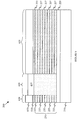
- FIG. 9 illustrates an optical fiber communication systems, which may form one environment where the completed optoelectronic device may be included.
- FIG. 10 illustrates an alternative optical fiber communication system.
- the optoelectronic device 100 is specifically discussed as a group III through group V based device, for example an indium phosphide/indium gallium arsenide phosphide based device, a gallium arsenide based device, an aluminum gallium arsenide based device, or another group III through group V based device.
- group III through group V based device for example an indium phosphide/indium gallium arsenide phosphide based device, a gallium arsenide based device, an aluminum gallium arsenide based device, or another group III through group V based device.
- group III through group V based device for example an indium phosphide/indium gallium arsenide phosphide based device, a gallium arsenide based device, an aluminum gallium arsenide based device, or another group III through group V based device.
- the present invention is discussed in the context of a group III through group V based device
- the optoelectronic device 100 includes a substrate 110 , a lower buffer layer 120 and a conventional active region 130 .
- the active region 130 may, as illustrated, comprise a multi quantum well structure, including separate confining layers, for example barrier layers 133 and quantum wells 137 .
- the active region 130 comprises five barrier layers 133 and four quantum wells 137 . It should be noted, however, that the active region 130 could comprise more or less barrier layers 133 and quantum wells 137 than illustrated in FIG. 1, depending on the design.
- An upper buffer layer 140 and a capping layer 150 may be located over active region 130 .
- the optoelectronic device 100 further includes a separate confinement layer 160 located between the active region 130 and the upper buffer layer 140 .
- the optoelectronic device 100 also includes a first active region 170 and a second active region 180 .
- the first and second action regions 170 , 180 are configured to have or produce different wavelengths of light generated from an electrical pulse.
- the wavelength of a material may be defined as the lowest wavelength (or effective bandgap) of light that may be passed through that material to cause absorption of the light.
- the first active region 170 may be a laser and the second active region 180 may be a modulator.
- the first and second active regions 170 , 180 could comprise other devices, such as optical amplifiers, optical waveguides or other similar devices.
- FIGS. 2-7 illustrated is one embodiment produced by a method of manufacturing the optoelectronic device 100 , including a method of monolithic integration of multiple active regions on an optoelectronic substrate.
- FIG. 2 illustrates a cross-sectional view of a partially completed optoelectronic device 200 .
- the partially completed optoelectronic device illustrated in FIG. 2 includes a lower buffer layer 220 , which in a previous step (not shown) was formed over an optoelectronic substrate 210 , which may be any layer located in an optoelectronic device.
- the optoelectronic substrate 210 in the exemplary embodiment shown in FIGS. 2-7, is a highly n-doped indium phosphide (InP) optoelectronic substrate.
- InP indium phosphide
- the lower buffer layer 220 located over the optoelectronic substrate 210 may be the lower buffer layer 220 .
- the lower buffer layer 220 in the illustrative embodiment, is an n-doped InP buffer layer having a thickness of about 500 nm. It should be noted, however, that the lower buffer layer 220 is not limited to an n-doped InP layer, and that other materials, doped or undoped, may be used.
- Formed over the lower buffer layer 220 is an active region 230 .
- the active region 230 as previously mentioned during the discussion of FIG. 1, may be a conventional multi quantum well structure, including barrier layers 233 and quantum wells 237 .
- the active region 230 includes materials chosen from group III through group V compounds.
- the active region 230 is typically intentionally not doped, however, in an alternative embodiment it may be doped as long as the p-n junction placement is taken into consideration.
- the barrier layers 233 have a thickness ranging from about 6 nm to about 8 nm and a given wavelength of about 1.24 ⁇ m
- the quantum wells 237 have a thickness ranging from about 6 nm to about 8 nm and a given wavelength of about 1.55 ⁇ m.
- the optoelectronic substrate 210 , lower buffer layer 220 and active region 230 may typically be formed using conventional processes, including but not limited to metalorganic vapor-phase epitaxy (MOVPE), epitaxial processes, or other similar processes. Also illustrated in FIG. 2, are proposed first and second active device regions 240 , 250 , respectively.
- MOVPE metalorganic vapor-phase epitaxy
- FIG. 2 Also illustrated in FIG. 2, are proposed first and second active device regions 240 , 250 , respectively.
- the cladding layer 310 is formed on the active region 230 .
- the cladding layer 310 is an undoped InP cladding layer.
- the cladding layer 310 may be doped, and more specifically, doped with a p-type dopant, such as zinc, which may diffuse very easily in subsequent processing steps.
- the cladding layer 310 may, in an exemplary embodiment, have a thickness ranging from about 0.1 nm to about 0.2 nm and may be formed using any conventional process.
- FIGS. 4A and 4B illustrated is a cross-sectional view and a top view, respectively, of the partially completed optoelectronic device 200 illustrated in FIG. 3, after formation of a mask portion 410 .
- the mask portion 410 may be formed over an area of the active region 230 where the proposed first active device region 240 is.
- the presence of the mask portion 410 forms a masked active region 413 and an unmasked active region 417 .
- the mask portion 410 substantially inhibits a shift in effective wavelength of the active region 230 located thereunder, during a subsequent processing step.
- One having skill in the art generally understands how to form the mask portion 410 . Referring specifically to FIG.
- the mask portion has a length 420 b substantially equal to a length of the desired first active region 170 (FIG. 1 ).
- the mask portion 410 may have a width 430 b substantially equal to a width of the desired first active region 170 .
- the length of the mask portion 410 might range from about 300 ⁇ m to about 400 ⁇ m and the width might be about 6 ⁇ m.
- FIG. 5 illustrates the formation of an optional etch stop layer 510 over the surface of the active region 230 except where the masked active region 413 is located.
- the etch stop layer 510 which may be an indium gallium arsenide phosphide or other similar layer, provides a barrier between the indium phosphide layer 310 and an N-Type doped layer, which is formed in a subsequent step. It should be noted that the etch stop layer 510 may be formed using a known process that is consistent with the present invention, including metalorganic vapor phase epitaxy (MOVPE).
- MOVPE metalorganic vapor phase epitaxy
- the N-type doped layer 610 which in the illustrative embodiment is an N-type indium phosphide layer, substantially alters the effective wavelength of the active region 230 located thereunder and forms a first active region 620 having the given wavelength and a second active region 630 having an altered wavelength different from the given wavelength.
- variations in a growth rate, a dopant concentration, a deposition temperature or mask geometry may affect how much the N-type doped layer 610 alters the wavelength of the second active region 630 .
- the growth rate may range from about 0.5 ⁇ m/hour to about 3.5 ⁇ m/hour
- the dopant concentration may range from about 1E18/cm 3 to about 4E18/cm 3
- the formation temperature may range from about 600° C. to about 680° C.
- the N-type doped layer 610 may be formed at a pressure of 1 atmosphere or less, and to a thickness ranging from about 1 ⁇ m to about 2 ⁇ m.
- the N-type doped layer 610 may be formed using many processes including metalorganic vapor deposition (MOCVD), chemical beam epitaxy (CBE), hydride vapor phase epitaxy (HVPE), liquid phase epitaxy (LPE), or another similar process.
- MOCVD metalorganic vapor deposition
- CBE chemical beam epitaxy
- HVPE hydride vapor phase epitaxy
- LPE liquid phase epitaxy
- the N-type doped layer 610 that is formed over the active region 230 may be used to form a first active region 620 comprising a laser and a second active region 630 comprising a modulator.
- the first active region 620 is a laser and has a given wavelength of about 1.55 ⁇ m
- the second active region 630 could be a modulator that has an altered wavelength of about 1.45 ⁇ m.
- the altered wavelength in the second active region 630 may vary from the given wavelength in the first active region 620 by up to about 0.2 ⁇ m.
- FIG. 7 illustrated is the partially completed optoelectronic device 200 illustrated in FIG. 6, including the first active region 620 and second active region 630 , after removal of the N-type doped layer 610 , etch stop layer 510 and mask portion 410 .
- the N-type doped layer 610 and etch stop layer 510 may be removed prior to removing the mask portion 410 .
- Many techniques may be used to remove the N-type doped layer 610 .
- a selective etch or other similar technique may be used to remove the N-type doped layer 610 , stopping on the etch stop layer 510 .
- a selective etch capable of removing the etch stop layer 510 may be conducted to remove the etch stop layer 510 .
- the mask portion 410 may be removed using a conventional removal process.
- the upper buffer layer 810 in an advantageous embodiment, is a P-type indium phosphide upper buffer layer. Since the P-type dopant may be introduced into the partially completed optoelectronic device 200 at such a late processing step, the amount of zinc diffusion therein and amount of damage caused therefrom is substantially minimized.
- the capping layer 150 may be formed, resulting in the completed optoelectronic device 100 illustrated in FIG. 1 .
- the capping layer 150 may comprise a P-type indium gallium arsenide layer.
- other materials, and various and conventional processing techniques, may be used to form the capping layer 150 .
- the currently discussed method for monolithic integration of multiple devices on an optoelectronic substrate allows easy and accurate formation of multiple devices having varying effective wavelengths on the optoelectronic substrate. Furthermore, the present method allows for an accurate and selective shift in effective wavelength depending on the growth rate of the N-type doped layer 610 and concentration of dopants within such a layer 610 . Likewise, the present method also allows for an accurate shift of effective wavelength up to about 0.2 ⁇ m, which is currently not available in the prior art methods. It should also be mentioned that the present inventive method may be combined with other applications, including but not limited to selective area growth.
- the optical fiber communication system 900 includes an initial signal 910 entering a receiver 920 .
- the receiver 920 receives the initial signal 910 , addresses the signal 910 and sends the resulting information across an optical fiber 930 to a transmitter 940 .
- the transmitter 940 receives the information from the optical fiber 930 , addresses the information and sends an ultimate signal 950 .
- the completed optoelectronic device 100 may be included within the receiver 920 .
- the completed optoelectronic device 100 may also be included anywhere in the optical fiber communication system 900 , including the transmitter 940 .
- the optical fiber communication system 900 is not limited to the devices previously mentioned.
- the optical fiber communication system 900 may include a source 960 , such as a laser or a diode.
- FIG. 10 illustrated is an alternative optical fiber communication system 1000 , having a repeater 1010 , including a second receiver 1020 and a second transmitter 1030 , located between the receiver 1020 and the transmitter 1040 .
Abstract
Description
Claims (20)
Priority Applications (1)
| Application Number | Priority Date | Filing Date | Title |
|---|---|---|---|
| US09/821,212 US6503768B2 (en) | 2001-03-29 | 2001-03-29 | Method for monolithic integration of multiple devices on an optoelectronic substrate |
Applications Claiming Priority (1)
| Application Number | Priority Date | Filing Date | Title |
|---|---|---|---|
| US09/821,212 US6503768B2 (en) | 2001-03-29 | 2001-03-29 | Method for monolithic integration of multiple devices on an optoelectronic substrate |
Publications (2)
| Publication Number | Publication Date |
|---|---|
| US20020173063A1 US20020173063A1 (en) | 2002-11-21 |
| US6503768B2 true US6503768B2 (en) | 2003-01-07 |
Family
ID=25232816
Family Applications (1)
| Application Number | Title | Priority Date | Filing Date |
|---|---|---|---|
| US09/821,212 Expired - Lifetime US6503768B2 (en) | 2001-03-29 | 2001-03-29 | Method for monolithic integration of multiple devices on an optoelectronic substrate |
Country Status (1)
| Country | Link |
|---|---|
| US (1) | US6503768B2 (en) |
Cited By (5)
| Publication number | Priority date | Publication date | Assignee | Title |
|---|---|---|---|---|
| US20030210723A1 (en) * | 2002-05-10 | 2003-11-13 | Adams David M. | Monolithically integrated high power laser optical device |
| US20040013154A1 (en) * | 2002-07-16 | 2004-01-22 | Applied Optoelectronics, Inc. | Optically-pumped multiple-quantum well active region with improved distribution of optical pumping power |
| US20070064296A1 (en) * | 2004-12-09 | 2007-03-22 | Fathimulla Ayub M | Modulating retroreflector array using vertical cavity optical amplifiers |
| US20080317422A1 (en) * | 2007-06-20 | 2008-12-25 | Takeshi Kitatani | Optical integrated device and manufacturing method thereof |
| US8470652B1 (en) | 2011-05-11 | 2013-06-25 | Hrl Laboratories, Llc | Monolithic integration of group III nitride enhancement layers |
Citations (6)
| Publication number | Priority date | Publication date | Assignee | Title |
|---|---|---|---|---|
| US5689600A (en) * | 1995-01-20 | 1997-11-18 | Minnesota Mining And Manufacturing Company | Electronic circuit structure |
| US5795798A (en) * | 1996-11-27 | 1998-08-18 | The Regents Of The University Of California | Method of making full color monolithic gan based leds |
| US5920766A (en) * | 1998-01-07 | 1999-07-06 | Xerox Corporation | Red and blue stacked laser diode array by wafer fusion |
| US6001664A (en) * | 1996-02-01 | 1999-12-14 | Cielo Communications, Inc. | Method for making closely-spaced VCSEL and photodetector on a substrate |
| US6174749B1 (en) * | 1998-05-13 | 2001-01-16 | The Regents Of The University Of California | Fabrication of multiple-wavelength vertical-cavity opto-electronic device arrays |
| US6282220B1 (en) * | 1998-01-07 | 2001-08-28 | Xerox Corporation | Red, infrared, and blue stacked laser diode array by water fusion |
-
2001
- 2001-03-29 US US09/821,212 patent/US6503768B2/en not_active Expired - Lifetime
Patent Citations (6)
| Publication number | Priority date | Publication date | Assignee | Title |
|---|---|---|---|---|
| US5689600A (en) * | 1995-01-20 | 1997-11-18 | Minnesota Mining And Manufacturing Company | Electronic circuit structure |
| US6001664A (en) * | 1996-02-01 | 1999-12-14 | Cielo Communications, Inc. | Method for making closely-spaced VCSEL and photodetector on a substrate |
| US5795798A (en) * | 1996-11-27 | 1998-08-18 | The Regents Of The University Of California | Method of making full color monolithic gan based leds |
| US5920766A (en) * | 1998-01-07 | 1999-07-06 | Xerox Corporation | Red and blue stacked laser diode array by wafer fusion |
| US6282220B1 (en) * | 1998-01-07 | 2001-08-28 | Xerox Corporation | Red, infrared, and blue stacked laser diode array by water fusion |
| US6174749B1 (en) * | 1998-05-13 | 2001-01-16 | The Regents Of The University Of California | Fabrication of multiple-wavelength vertical-cavity opto-electronic device arrays |
Cited By (13)
| Publication number | Priority date | Publication date | Assignee | Title |
|---|---|---|---|---|
| US20030210723A1 (en) * | 2002-05-10 | 2003-11-13 | Adams David M. | Monolithically integrated high power laser optical device |
| US7035305B2 (en) * | 2002-05-10 | 2006-04-25 | Bookham Technology, Plc | Monolithically integrated high power laser optical device |
| US20040013154A1 (en) * | 2002-07-16 | 2004-01-22 | Applied Optoelectronics, Inc. | Optically-pumped multiple-quantum well active region with improved distribution of optical pumping power |
| US6859481B2 (en) * | 2002-07-16 | 2005-02-22 | Applied Optoelectronics, Inc. | Optically-pumped multiple-quantum well active region with improved distribution of optical pumping power |
| US20070064296A1 (en) * | 2004-12-09 | 2007-03-22 | Fathimulla Ayub M | Modulating retroreflector array using vertical cavity optical amplifiers |
| US7339726B2 (en) * | 2004-12-09 | 2008-03-04 | Epitaxial Technologies | Modulating retroreflector array using vertical cavity optical amplifiers |
| US20080317422A1 (en) * | 2007-06-20 | 2008-12-25 | Takeshi Kitatani | Optical integrated device and manufacturing method thereof |
| US7711229B2 (en) * | 2007-06-20 | 2010-05-04 | Opnext Japan, Inc. | Optical integrated device and manufacturing method thereof |
| US8470652B1 (en) | 2011-05-11 | 2013-06-25 | Hrl Laboratories, Llc | Monolithic integration of group III nitride enhancement layers |
| US8796736B1 (en) | 2011-05-11 | 2014-08-05 | Hrl Laboratories, Llc | Monolithic integration of group III nitride epitaxial layers |
| US9378949B1 (en) | 2011-05-11 | 2016-06-28 | Hrl Laboratories, Llc | Monolithic integration of group III nitride epitaxial layers |
| US9954090B1 (en) | 2011-05-11 | 2018-04-24 | Hrl Laboratories, Llc | Monolithic integration of group III nitride epitaxial layers |
| US10418473B1 (en) | 2011-05-11 | 2019-09-17 | Hrl Laboratories, Llc | Monolithic integration of group III nitride epitaxial layers |
Also Published As
| Publication number | Publication date |
|---|---|
| US20020173063A1 (en) | 2002-11-21 |
Similar Documents
| Publication | Publication Date | Title |
|---|---|---|
| CA2155776A1 (en) | Method for a reflective digitally tunable laser | |
| EP1719003B1 (en) | Buried heterostructure device fabricated by single step mocvd | |
| JP2005333144A (en) | Photonic integrated device using reverse-mesa structure and method for fabricating same | |
| JPH0864906A (en) | Manufacture of semiconductor device | |
| EP3963677A1 (en) | Monolithically integrated gain element | |
| US6503768B2 (en) | Method for monolithic integration of multiple devices on an optoelectronic substrate | |
| KR100337704B1 (en) | The manufacturing method for electro-absorption modulator intergrated laser | |
| US5610095A (en) | Monolithically integrated circuits having dielectrically isolated, electrically controlled optical devices and process for fabricating the same | |
| US20050185689A1 (en) | Optoelectronic device having a Discrete Bragg Reflector and an electro-absorption modulator | |
| US20020090167A1 (en) | Electronic device having a barrier region including aluminum and a method of manufacture therefor | |
| JPH09237940A (en) | Semiconductor device and manufacture thereof | |
| US6771869B2 (en) | Optoelectronic device having a barrier layer associated therewith and a method of manufacture thereof | |
| US6780241B2 (en) | Monolithic optical device manufacturing and integration methods | |
| US20200381899A1 (en) | Semiconductor device with Selective Area Epitaxy growth utilizing a mask to suppress or enhance growth at the edges | |
| US6542686B1 (en) | Optoelectronic device including a barrier layer and interface barrier layer and a method of manufacture thereof | |
| CN114899697B (en) | Dual-wavelength cascade semiconductor laser and preparation method thereof | |
| JPH05102607A (en) | Manufacture of buried structure semiconductor laser | |
| KR100248430B1 (en) | Structure and fabrication method of passive-waveguide integrated laser diode | |
| WO2021209115A1 (en) | Electroabsorption modulated laser | |
| JP2002252406A (en) | Ribbon embedded semiconductor laser and its manufacturing method | |
| KR100909974B1 (en) | Semiconductor laser diode for wdm-pon system and its manufacturing method | |
| JPH0697591A (en) | Manufacture of semiconductor laser | |
| KR100275520B1 (en) | Radial Angle Adjustable Planar Embedded Semiconductor Laser Device | |
| WO2001052374A1 (en) | Electronic device having a barrier region including aluminum and a method of manufacture therefor | |
| JP2002151785A (en) | Optical semiconductor device and its manufacturing method |
Legal Events
| Date | Code | Title | Description |
|---|---|---|---|
| AS | Assignment |
Owner name: AGERE SYSTEMS OPTOELECTRONICS GUARDIAN CORPORATION Free format text: ASSIGNMENT OF ASSIGNORS INTEREST;ASSIGNORS:CHO, SI HYUNG;LEIBENGUTH, RONALD E.;OUGAZZADEN, ABDALLAH;AND OTHERS;REEL/FRAME:011703/0034;SIGNING DATES FROM 20010220 TO 20010315 |
|
| FEPP | Fee payment procedure |
Free format text: PAYOR NUMBER ASSIGNED (ORIGINAL EVENT CODE: ASPN); ENTITY STATUS OF PATENT OWNER: LARGE ENTITY |
|
| STCF | Information on status: patent grant |
Free format text: PATENTED CASE |
|
| FPAY | Fee payment |
Year of fee payment: 4 |
|
| FPAY | Fee payment |
Year of fee payment: 8 |
|
| AS | Assignment |
Owner name: DEUTSCHE BANK AG NEW YORK BRANCH, AS COLLATERAL AG Free format text: PATENT SECURITY AGREEMENT;ASSIGNORS:LSI CORPORATION;AGERE SYSTEMS LLC;REEL/FRAME:032856/0031 Effective date: 20140506 |
|
| FPAY | Fee payment |
Year of fee payment: 12 |
|
| AS | Assignment |
Owner name: AGERE SYSTEMS GUARDIAN CORP., PENNSYLVANIA Free format text: MERGER;ASSIGNOR:AGERE SYSTEMS OPTOELECTRONICS GUARDIAN CORP.;REEL/FRAME:035000/0029 Effective date: 20010823 Owner name: AVAGO TECHNOLOGIES GENERAL IP (SINGAPORE) PTE. LTD Free format text: ASSIGNMENT OF ASSIGNORS INTEREST;ASSIGNOR:AGERE SYSTEMS LLC;REEL/FRAME:035059/0001 Effective date: 20140804 Owner name: AGERE SYSTEMS LLC, PENNSYLVANIA Free format text: MERGER;ASSIGNOR:AGERE SYSTEMS INC.;REEL/FRAME:035058/0895 Effective date: 20120724 Owner name: AGERE SYSTEMS INC., PENNSYLVANIA Free format text: MERGER;ASSIGNOR:AGERE SYSTEMS GUARDIAN CORP.;REEL/FRAME:035058/0884 Effective date: 20020822 |
|
| AS | Assignment |
Owner name: LSI CORPORATION, CALIFORNIA Free format text: TERMINATION AND RELEASE OF SECURITY INTEREST IN PATENT RIGHTS (RELEASES RF 032856-0031);ASSIGNOR:DEUTSCHE BANK AG NEW YORK BRANCH, AS COLLATERAL AGENT;REEL/FRAME:037684/0039 Effective date: 20160201 Owner name: AGERE SYSTEMS LLC, PENNSYLVANIA Free format text: TERMINATION AND RELEASE OF SECURITY INTEREST IN PATENT RIGHTS (RELEASES RF 032856-0031);ASSIGNOR:DEUTSCHE BANK AG NEW YORK BRANCH, AS COLLATERAL AGENT;REEL/FRAME:037684/0039 Effective date: 20160201 |
|
| AS | Assignment |
Owner name: BANK OF AMERICA, N.A., AS COLLATERAL AGENT, NORTH CAROLINA Free format text: PATENT SECURITY AGREEMENT;ASSIGNOR:AVAGO TECHNOLOGIES GENERAL IP (SINGAPORE) PTE. LTD.;REEL/FRAME:037808/0001 Effective date: 20160201 Owner name: BANK OF AMERICA, N.A., AS COLLATERAL AGENT, NORTH Free format text: PATENT SECURITY AGREEMENT;ASSIGNOR:AVAGO TECHNOLOGIES GENERAL IP (SINGAPORE) PTE. LTD.;REEL/FRAME:037808/0001 Effective date: 20160201 |
|
| AS | Assignment |
Owner name: AVAGO TECHNOLOGIES GENERAL IP (SINGAPORE) PTE. LTD., SINGAPORE Free format text: TERMINATION AND RELEASE OF SECURITY INTEREST IN PATENTS;ASSIGNOR:BANK OF AMERICA, N.A., AS COLLATERAL AGENT;REEL/FRAME:041710/0001 Effective date: 20170119 Owner name: AVAGO TECHNOLOGIES GENERAL IP (SINGAPORE) PTE. LTD Free format text: TERMINATION AND RELEASE OF SECURITY INTEREST IN PATENTS;ASSIGNOR:BANK OF AMERICA, N.A., AS COLLATERAL AGENT;REEL/FRAME:041710/0001 Effective date: 20170119 |
|
| AS | Assignment |
Owner name: AVAGO TECHNOLOGIES INTERNATIONAL SALES PTE. LIMITE Free format text: MERGER;ASSIGNOR:AVAGO TECHNOLOGIES GENERAL IP (SINGAPORE) PTE. LTD.;REEL/FRAME:047195/0026 Effective date: 20180509 |
|
| AS | Assignment |
Owner name: AVAGO TECHNOLOGIES INTERNATIONAL SALES PTE. LIMITE Free format text: CORRECTIVE ASSIGNMENT TO CORRECT THE EFFECTIVE DATE OF MERGER PREVIOUSLY RECORDED ON REEL 047195 FRAME 0026. ASSIGNOR(S) HEREBY CONFIRMS THE MERGER;ASSIGNOR:AVAGO TECHNOLOGIES GENERAL IP (SINGAPORE) PTE. LTD.;REEL/FRAME:047477/0423 Effective date: 20180905 |