US6495389B2 - Method for manufacturing semiconductor pressure sensor having reference pressure chamber - Google Patents
Method for manufacturing semiconductor pressure sensor having reference pressure chamber Download PDFInfo
- Publication number
- US6495389B2 US6495389B2 US09/924,559 US92455901A US6495389B2 US 6495389 B2 US6495389 B2 US 6495389B2 US 92455901 A US92455901 A US 92455901A US 6495389 B2 US6495389 B2 US 6495389B2
- Authority
- US
- United States
- Prior art keywords
- pressure chamber
- semiconductor substrate
- reference pressure
- diaphragm
- heat treatment
- Prior art date
- Legal status (The legal status is an assumption and is not a legal conclusion. Google has not performed a legal analysis and makes no representation as to the accuracy of the status listed.)
- Expired - Lifetime
Links
Images


Classifications
-
- B—PERFORMING OPERATIONS; TRANSPORTING
- B81—MICROSTRUCTURAL TECHNOLOGY
- B81C—PROCESSES OR APPARATUS SPECIALLY ADAPTED FOR THE MANUFACTURE OR TREATMENT OF MICROSTRUCTURAL DEVICES OR SYSTEMS
- B81C1/00—Manufacture or treatment of devices or systems in or on a substrate
- B81C1/00777—Preserve existing structures from alteration, e.g. temporary protection during manufacturing
- B81C1/00833—Methods for preserving structures not provided for in groups B81C1/00785 - B81C1/00825
-
- B—PERFORMING OPERATIONS; TRANSPORTING
- B81—MICROSTRUCTURAL TECHNOLOGY
- B81C—PROCESSES OR APPARATUS SPECIALLY ADAPTED FOR THE MANUFACTURE OR TREATMENT OF MICROSTRUCTURAL DEVICES OR SYSTEMS
- B81C1/00—Manufacture or treatment of devices or systems in or on a substrate
- B81C1/00015—Manufacture or treatment of devices or systems in or on a substrate for manufacturing microsystems
- B81C1/00023—Manufacture or treatment of devices or systems in or on a substrate for manufacturing microsystems without movable or flexible elements
- B81C1/00047—Cavities
-
- B—PERFORMING OPERATIONS; TRANSPORTING
- B81—MICROSTRUCTURAL TECHNOLOGY
- B81B—MICROSTRUCTURAL DEVICES OR SYSTEMS, e.g. MICROMECHANICAL DEVICES
- B81B2201/00—Specific applications of microelectromechanical systems
- B81B2201/02—Sensors
- B81B2201/0264—Pressure sensors
-
- B—PERFORMING OPERATIONS; TRANSPORTING
- B81—MICROSTRUCTURAL TECHNOLOGY
- B81B—MICROSTRUCTURAL DEVICES OR SYSTEMS, e.g. MICROMECHANICAL DEVICES
- B81B2203/00—Basic microelectromechanical structures
- B81B2203/01—Suspended structures, i.e. structures allowing a movement
- B81B2203/0127—Diaphragms, i.e. structures separating two media that can control the passage from one medium to another; Membranes, i.e. diaphragms with filtering function
-
- B—PERFORMING OPERATIONS; TRANSPORTING
- B81—MICROSTRUCTURAL TECHNOLOGY
- B81B—MICROSTRUCTURAL DEVICES OR SYSTEMS, e.g. MICROMECHANICAL DEVICES
- B81B2203/00—Basic microelectromechanical structures
- B81B2203/03—Static structures
- B81B2203/0315—Cavities
-
- B—PERFORMING OPERATIONS; TRANSPORTING
- B81—MICROSTRUCTURAL TECHNOLOGY
- B81C—PROCESSES OR APPARATUS SPECIALLY ADAPTED FOR THE MANUFACTURE OR TREATMENT OF MICROSTRUCTURAL DEVICES OR SYSTEMS
- B81C2201/00—Manufacture or treatment of microstructural devices or systems
- B81C2201/01—Manufacture or treatment of microstructural devices or systems in or on a substrate
- B81C2201/0101—Shaping material; Structuring the bulk substrate or layers on the substrate; Film patterning
- B81C2201/0111—Bulk micromachining
- B81C2201/0116—Thermal treatment for structural rearrangement of substrate atoms, e.g. for making buried cavities
-
- B—PERFORMING OPERATIONS; TRANSPORTING
- B81—MICROSTRUCTURAL TECHNOLOGY
- B81C—PROCESSES OR APPARATUS SPECIALLY ADAPTED FOR THE MANUFACTURE OR TREATMENT OF MICROSTRUCTURAL DEVICES OR SYSTEMS
- B81C2201/00—Manufacture or treatment of microstructural devices or systems
- B81C2201/01—Manufacture or treatment of microstructural devices or systems in or on a substrate
- B81C2201/0174—Manufacture or treatment of microstructural devices or systems in or on a substrate for making multi-layered devices, film deposition or growing
- B81C2201/019—Bonding or gluing multiple substrate layers
Definitions
- This invention relates to a method for manufacturing a semiconductor pressure sensor having a closed cavity formed in a semiconductor substrate as a reference pressure chamber.
- Methods for manufacturing this kind of semiconductor pressure sensors are proposed by, for example, JP-A-8-236788, JP-A-6-18345, and JP-A-11-298009. These methods are as follows.
- a cavity is formed on a surface of a semiconductor substrate made of silicon or the like.
- another substrate made of semiconductor or the like is bonded to the surface of the semiconductor substrate to close the cavity.
- a heat treatment is performed to the substrates.
- the two substrates are securely bonded, and a reference pressure chamber is provided with a predetermined internal pressure.
- a diaphragm for detecting a-pressure is formed from the semiconductor substrate at a portion corresponding to the reference pressure chamber, i.e., corresponding to a bottom portion of the cavity.
- the elements such as the strain gauges and the integrated circuit are formed in the semiconductor substrate.
- the semiconductor substrate is heated for performing ion-implantation, diffusion, and the like. If temperatures of such heat treatments are too high, the internal pressure of the reference pressure chamber is increased to deform the diaphragm.
- the deformation of the diaphragm is accompanied by crystal defects thereof that are produced where stress concentrates on.
- crystal defects are liable to be produced especially at an edge portion of the diaphragm.
- electrical leakage and mechanical leakage easily occur to hamper the element formation.
- the diaphragm may be damaged, and pressure may leak from the reference pressure chamber.
- An object of the present invention is to prevent crystal defects from being produced in a diaphragm of a semiconductor pressure sensor having a reference pressure chamber in a semiconductor substrate.
- a reference pressure chamber is formed by closing a cavity formed in a semiconductor substrate, and a diaphragm is formed from a part of the semiconductor substrate corresponding to the reference pressure chamber.
- a first heat treatment is then performed to the semiconductor substrate, at a first temperature T 1 that satisfies a relation of:
- P 0 is an internal pressure (atm) of the reference pressure chamber at a room temperature. Accordingly, crystal defects can be prevented from being produced in the diaphragm.
- the internal pressure of the reference pressure chamber can be controlled by temperature and pressure for forming the reference pressure chamber, which are determined using the Boyle-Charles's law.
- the first heat treatment may be performed to form strain gauges, an insulation film, an integrated circuit or the like on the semiconductor substrate.
- the reference pressure chamber is formed by performing a second heat treatment at a second temperature T 2 that satisfies a relation of:
- P 0 is the internal pressure of the reference pressure chamber at the room temperature. Accordingly, even when the diaphragm is formed simultaneously with the reference pressure chamber, crystal defects can be prevented from being produced in the thin diaphragm securely.
- FIG. 1 is a cross-sectional view showing a semiconductor pressure sensor according to a first preferred embodiment of the present invention
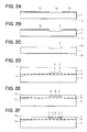
- FIGS. 2A to 2 F are cross-sectional views showing a method for manufacturing the semiconductor pressure sensor shown in FIG. 1 in a stepwise manner;
- FIG. 3 is a graph showing existence of crystal defects produced in a diaphragm at various heat treatment temperatures and various internal pressures of a cavity;
- FIG. 4 is a cross-sectional view showing a semiconductor pressure sensor according to a second preferred embodiment of the present invention.
- FIGS. 5A to 5 D are cross-sectional views showing a method for manufacturing the semiconductor pressure sensor shown in FIG. 4 in a stepwise-manner.
- a semiconductor pressure sensor S 1 according to a first preferred embodiment of the present invention is explained referring to FIG. 1 .
- the semiconductor pressure sensor S 1 has a semiconductor substrate 1 composed of an n-type single crystal silicon substrate having a (100) plane orientation.
- a cavity 2 is formed in the semiconductor substrate 1 as a recess from a surface 1 a of the semiconductor substrate 1 .
- another substrate (base substrate) 3 made of semiconductor, glass, or the like is bonded to the surface 1 a of the semiconductor substrate 1 with a silicon oxide film 4 interposed therebetween, and closes the cavity 2 .
- the substrate 3 is a single crystal silicon substrate similarly to the semiconductor substrate 1 .
- the cavity 2 defines a closed space by the bonding of the substrate 3 , and the space works as a reference pressure chamber 5 having a predetermined internal pressure.
- a diaphragm 6 for detecting a pressure is formed as a thin part of the semiconductor substrate 1 corresponding to the reference pressure chamber 5 , at the bottom side of the cavity 2 .
- the thickness of the diaphragm 6 is not limited to a specific magnitude, but is applicable in a range from a thin thickness (for example, about several ⁇ m) at which the flexure theory can be adopted (where a relation between a pressure applied to the diaphragm and a maximum flexure of the diaphragm is nonlinear), to a relatively large thickness.
- the internal pressure of the reference pressure chamber 5 can be controlled to be about 0.6 atm or less at a room temperature.
- strain gauges 7 are formed on a surface 1 b of the semiconductor substrate 1 opposed to the surface 1 a , where the diaphragm 6 is formed.
- the strain gauges 7 constitute a bridge circuit to output an electrical signal corresponding to stress that is produced when the diaphragm 6 is strained.
- the strain gauges 7 are formed from a p + layer in this embodiment.
- the surface 1 b of the semiconductor substrate 1 is then covered with an insulation film (such as an oxide film) 8 , and electrodes 9 are formed on the insulation film 8 to be electrically connected to the strain gauges 7 through contact holes formed in the insulation film 8 .
- the electrodes 9 include a wiring member for externally outputting the electrical signal from the strain gauges 7 and pads for wire bonding.
- the above-described semiconductor pressure sensor S 1 is an absolute-pressure sensor having the reference pressure chamber 5 , and outputs the electrical signal from the strain gauges 7 in accordance with the strain produced when the diaphragm 6 is deformed upon receiving a pressure at a side of the surface 1 b of the semiconductor substrate 1 .
- the signal from the strain gauges 7 is outputted, through the electrodes 9 as the wiring member and the pads, to a signal processing circuit or the like that is provided-at an outside. Thus, the pressure is detected.
- the semiconductor substrate (n-type (100) single crystal silicon substrate in this embodiment) 1 is prepared, and an oxide film (silicon oxide film) 10 is deposited on the surface 1 a of the semiconductor substrate 1 by thermal oxidation. After that, the oxide film 10 is patterned to be open at a region where the cavity 2 is to be formed (oxide film formation step).
- a heat treatment is performed at, for example, in a range of 1100° C. to 1150° C. to enhance the bonding strength of the two substrates 1 , 3 .
- the two substrates 1 , 3 are bonded together through the oxide film 4 in a convalent bond, and the reference pressure chamber 5 is defined (reference pressure chamber formation step).
- the ambient pressure when the two substrates 1 , 3 are bonded is determined based on the Boyle-Charles's law so that the reference pressure chamber 5 has a desired internal pressure at a room temperature.
- the ambient pressure at the bonding is controlled to be about 10 ⁇ 6 Torr (133 ⁇ 10 ⁇ 6 Pa).
- the internal pressure of the reference pressure chamber 5 should be controlled so that stress (maximum stress) applied to the edge portions of the diaphragm 6 does not exceed a breaking stress (strength) of silicon.
- the internal pressure of the reference pressure chamber 5 is preferably controlled to be 3.2 atm or less at the room temperature. Therefore, the heat treatment temperature in the reference pressure chamber formation step is controlled so that the reference pressure chamber 5 has an internal pressure of 3.2 atm or less (for example, 0.6 atm) at the room temperature.
- the semiconductor substrate 1 is thinned from the side of the surface 1 b to form the diaphragm 6 (diaphragm formation step).
- This thinning step can be performed by grinding and polishing or by wet etching of silicon.
- the strain gauges 7 are formed on the surface 1 b of the semiconductor substrate 1 by forming a p + layer in which boron is diffused.
- the insulation film 8 is formed by thermal oxidation, and the electrodes 9 are formed by deposition or sputtering of aluminum.
- the strain gauges 7 , the insulation film 8 , the electrodes 9 , and, if necessary, elements such as an integrated circuit are formed on the semiconductor substrate 1 , so that the semiconductor pressure sensor S 1 shown in FIG. 1 is completed.
- heat treatments are performed with respect to the semiconductor substrate 1 .
- temperature (heat treatment temperature) T 1 of the heat treatment that is performed to the semiconductor substrate 1 after the reference pressure chamber 5 is formed is 1150° C.
- temperature T 2 of the heat treatment that is performed when the reference pressure chamber 5 is formed is in a range of about 1100° C. to 1150° C.
- the following experiments were performed to prevent occurrence of crystal detects in the diaphragm 6 .
- the above-described steps were performed to the diaphragm formation step, and several sensor samples (sub-works) were manufactured to have various internal pressures (atm) of the reference pressure chamber 5 at the room temperature (25° C.). Then, after the respective sub-works were exposed to various heat treatment temperatures, they were examined by using SEM, TEM, and the like to check the occurrence of crystal defects in the diaphragm 6 .
- crystal defects are mainly dislocations induced in a crystal lattice structure (lattice structure of single crystal silicon) of the semiconductor substrate 1 .
- stress of the diaphragm 6 exceeds a yield stress so that the diaphragm 6 is plastically deformed to have dislocations therein.
- FIG. 3 shows existence of crystal defects at various internal pressures of the reference pressure chamber (cavity internal pressure) at the room temperature and various heat treatment temperatures.
- a horizontal axis indicates cavity internal pressures (atm) and a vertical axis indicates heat treatment temperatures (° C.).
- Mark O represents a case where no crystal defect exists, while mark X represents a case where crystal defects exist.
- a boundary that divides whether crystal defects are produced or not is linear in the relation between the cavity internal pressure and the heat treatment temperature. That is, crystal defects are produced in the upper region of the straight line L 1 as the boundary, and are not produced in the lower region of the straight line L 1 .
- the heat treatment temperature in FIG. 3 corresponds to the temperature of the heat treatment that is performed to the semiconductor substrate 1 after the reference pressure chamber 5 is formed. Therefore, the straight line L 1 is represented by formula ( 1 ).
- T 1 ⁇ 430P 0 +1430 (1)
- T 1 is the temperature of the heat treatment performed to the semiconductor substrate 1 after the reference pressure cavity 5 is formed
- P 0 is the internal pressure (atm) of the reference pressure chamber 5 .
- the heat treatment temperature T 1 and the internal pressure P 0 should be in the lower region of the straight line L 1 in order to prevent occurrence of crystal defects in the diaphragm 6 .
- the heat treatment temperature T 1 should be lower than ( ⁇ 430P 0 +1430)° C. when the heat treatment is performed to the semiconductor substrate 1 to form the elements such as the strain gauges 7 and the integrated circuit or to do other things after the reference pressure cavity 5 is formed.
- the results shown in FIG. 3 apply to the temperature T 2 of the heat treatment that is performed to the semiconductor substrate when the reference pressure chamber 5 is formed (in the reference pressure chamber formation step). That is, when the heat treatment temperature T 2 is lower than ( ⁇ 430P 0 +1430)° C., the bottom surface portion of the cavity 2 that is to from the diaphragm 6 can be prevented from being deformed to have crystal defects therein in the reference pressure chamber formation step. In consequence, crystal defects can be prevented from being produced in the diaphragm 6 .
- the bottom surface portion of the cavity formed in the reference pressure chamber formation step is a portion for forming the diaphragm 6 , the bottom surface portion is thicker than the final thickness of the diaphragm 6 . Therefore, the bottom surface portion is less liable to be deformed at the heat treatment temperature T 2 and less liable to have crystal defects therein in the reference pressure chamber formation step.
- the diaphragm 6 may be formed at the cavity formation step without performing the diaphragm formation step.
- anisotropic etching or dry etching may be performed to form the cavity until the diaphragm 6 is formed with a final desired thickness.
- the reference pressure chamber formation step is performed to the semiconductor substrate 1 having the thin diaphragm 6 .
- the diaphragm 6 becomes liable to be plastically deformed easily to have crystal defects therein at the heat treatment temperature T 2 when the substrates 1 , 3 are bonded to form the reference pressure chamber 5 .
- the heat treatment temperature T 1 after the reference pressure chamber 5 is formed should be controlled to be lower than ( ⁇ 430P 0 +1430) because the heat treatment temperature T 2 largely affects the occurrence of crystal defects.
- a cavity can be formed in a semiconductor substrate by forming a trench having a large aspect ratio on the substrate in advance and by performing a heat treatment in a reduction atmosphere of hydrogen or the like to cause surface migration of silicon.
- a semiconductor pressure sensor S 2 in a second preferred embodiment shown in FIG. 4 is formed with a reference pressure chamber by utilizing the surface migration of silicon.
- FIG. 4 the same or similar parts as those shown in FIG. 1 are designated with the same reference numerals.
- a reference pressure chamber 5 is formed inside a semiconductor substrate 1 as a closed space, and a diaphragm 6 is formed as a thin portion at a side of the surface 1 a of the semiconductor substrate 1 corresponding to the reference pressure chamber 5 .
- strain gauges 7 composed of a p + layer, and an insulation film (oxide film) 8 are formed on the semiconductor substrate 1 , and electrodes 9 made of aluminum or the like are formed to be electrically connected to the strain gauges 7 through contact holes formed in the insulation film 8 .
- Elements such as an integrated circuit are optionally formed, and the surface of the sensor S 2 is covered with a protective film 11 made of silicon nitride (SiN) or the like.
- SiN silicon nitride
- the sensor S 2 can be manufactured by a manufacturing method as shown in FIGS. 5A to 5 D.
- the semiconductor substrate 1 made of silicon is prepared in FIG. 5 A.
- the surface 1 a of the semiconductor substrate 1 is covered with mask 14 made of a silicon oxide film having openings 13 open where several trenches 12 are to be formed.
- the mask 14 is removed by wet-etching using hydrogen fluoride (HF) or dry etching. Then, a heat treatment is performed to the semiconductor substrate 1 having the trenches 12 , in reduction atmosphere including hydrogen or the like, at a temperature of, for example, about 1100° C. to 1150° C.
- HF hydrogen fluoride
- the several trenches 12 are integrated to form a space as a whole inside the semiconductor substrate 1 and simultaneously the opening portions of the trenches 12 are closed (blocked) on the surface 1 a of the semiconductor substrate 1 , due to surface migration of silicon.
- the space formed inside the semiconductor substrate 1 works as the reference pressure chamber 5 , and the blocked portion forms the diaphragm 6 at the side of the surface 1 a of the semiconductor substrate 1 (reference chamber formation step).
- FIG. 5 D After that, the strain gauges, the insulation film, the electrodes, and the elements are formed on the semiconductor substrate 1 (element formation step).
- the semiconductor pressure sensor S 2 shown in FIG. 4 is completed.
- crystal defects can be prevented from being produced in the diaphragm 6 by setting the temperature T 1 of the heat treatment, which is performed to the semiconductor substrate 1 after the reference pressure chamber 5 is formed, to be lower than ( ⁇ 430P 0 +1430)° C.
- the strain gauges 7 are formed from a p 30 layer in which boron is diffused
- a heat treatment is performed at about 1050° C. to diffuse the boron.
- the insulation film 8 is formed from a silicon oxide film (SiO 2 )
- the insulation film 8 is formed by the heat treatment of about 1050° C.
- the electrodes 9 are made of aluminum, it is deposited at several hundreds degrees.
- the protective film 11 is made of SiN deposited by plasma CVD, a temperature of about 200° C. is applied during the formation of SiN.
- the thin diaphragm is formed in the reference pressure chamber formation step. Therefore, in order to prevent crystal defects from being produced in the diaphragm 6 sufficiently, not only the heat treatment temperature T 1 but also the heat treatment temperature T 2 , which is performed when the reference pressure chamber 5 is formed should be controlled to be lower than ( ⁇ 430P 0 +1430)° C. (for example, about 1100° C. to 1150° C.).
- the heat treatment is performed to the semiconductor substrate 1 that is placed in a sealed vessel (not shown) having reduction atmosphere such as hydrogen atmosphere.
- the pressure inside the sealed vessel is determined by controlling a flow rate of reduction gas flowing in the vessel and the like so that the internal pressure P 0 of the reference pressure chamber 5 finally has a desired value at the room temperature.
- the substrate 3 is not limited to a semiconductor substrate, but may be a glass substrate (glass base) or the like.
- the semiconductor substrate 1 and the substrate 3 are bonded together by anodic bonding at the heat treatment temperature T 2 as described above.
- each the semiconductor pressure sensors S 1 , S 2 is an absolute-pressure sensor having the reference pressure chamber 5
- the present invention is not limited to that.
- the present invention may be applied to relative pressure sensors as disclosed in JP-A-8-236788.
- a hole pressure conduction hole
- the diaphragm 6 receives the pressure introduced from the hole and the pressure applied to the surface 1 a of the semiconductor substrate 1 to detected a relative pressure therebetween.
Abstract
In a method for manufacturing a semiconductor pressure sensor, after a reference pressure chamber is formed inside a semiconductor substrate and a diaphragm is formed from a part of the semiconductor substrate, a heat treatment is performed to form an insulation film, an element, or the like on the semiconductor substrate. At that time, a heat treatment temperature is controlled to be lower than (-430P0+1430)° C. where P0 is an internal pressure (atm) of the reference pressure chamber at a room temperature. Accordingly, crystal defects can be prevented from being produced in the diaphragm.
Description
This application is based upon and claims the benefit of Japanese Patent Applications No. 2000-269079 filed on Sep. 5, 2000, No. 2001-4028 filed on Jan. 11, 2001, the contents of which are incorporated herein by reference.
1. Field of the Invention
This invention relates to a method for manufacturing a semiconductor pressure sensor having a closed cavity formed in a semiconductor substrate as a reference pressure chamber.
2. Description of the Related Art
Methods for manufacturing this kind of semiconductor pressure sensors are proposed by, for example, JP-A-8-236788, JP-A-6-18345, and JP-A-11-298009. These methods are as follows.
First, a cavity (recess) is formed on a surface of a semiconductor substrate made of silicon or the like. After that, another substrate made of semiconductor or the like is bonded to the surface of the semiconductor substrate to close the cavity. Then,a heat treatment is performed to the substrates. As a result, the two substrates are securely bonded, and a reference pressure chamber is provided with a predetermined internal pressure.
Further, a diaphragm for detecting a-pressure is formed from the semiconductor substrate at a portion corresponding to the reference pressure chamber, i.e., corresponding to a bottom portion of the cavity. After that, elements such as strain gauges and an integrated circuit a reformed in the semiconductor substrate by treatments such as diffusion and implantation. As a result, a semiconductor pressure sensor is completed.
According to studies and experiments by the inventors, however, it is revealed that the conventional manufacturing method has problems as follows.
Specifically, in the conventional method, after the closed cavity, i.e., the reference pressure chamber is formed in the semiconductor substrate, the elements such as the strain gauges and the integrated circuit are formed in the semiconductor substrate. In the steps following the formation of the reference pressure chamber, the semiconductor substrate is heated for performing ion-implantation, diffusion, and the like. If temperatures of such heat treatments are too high, the internal pressure of the reference pressure chamber is increased to deform the diaphragm.
The deformation of the diaphragm is accompanied by crystal defects thereof that are produced where stress concentrates on. For example, crystal defects are liable to be produced especially at an edge portion of the diaphragm. In the portion having crystal defects, electrical leakage and mechanical leakage easily occur to hamper the element formation. Further, the diaphragm may be damaged, and pressure may leak from the reference pressure chamber.
The present invention has been made in view of the above problems. An object of the present invention is to prevent crystal defects from being produced in a diaphragm of a semiconductor pressure sensor having a reference pressure chamber in a semiconductor substrate.
According to the present invention, in a method for manufacturing a semiconductor pressure sensor, a reference pressure chamber is formed by closing a cavity formed in a semiconductor substrate, and a diaphragm is formed from a part of the semiconductor substrate corresponding to the reference pressure chamber. A first heat treatment is then performed to the semiconductor substrate, at a first temperature T1 that satisfies a relation of:
where P0 is an internal pressure (atm) of the reference pressure chamber at a room temperature. Accordingly, crystal defects can be prevented from being produced in the diaphragm. The internal pressure of the reference pressure chamber can be controlled by temperature and pressure for forming the reference pressure chamber, which are determined using the Boyle-Charles's law.
The first heat treatment may be performed to form strain gauges, an insulation film, an integrated circuit or the like on the semiconductor substrate. Preferably, the reference pressure chamber is formed by performing a second heat treatment at a second temperature T2 that satisfies a relation of:
T 2<−430P0+1430
where P0 is the internal pressure of the reference pressure chamber at the room temperature. Accordingly, even when the diaphragm is formed simultaneously with the reference pressure chamber, crystal defects can be prevented from being produced in the thin diaphragm securely.
Other objects and features of the present invention will become more readily apparent from a better understanding of the preferred embodiments described below with reference to the following drawings, in which;
FIG. 1 is a cross-sectional view showing a semiconductor pressure sensor according to a first preferred embodiment of the present invention;
FIGS. 2A to 2F are cross-sectional views showing a method for manufacturing the semiconductor pressure sensor shown in FIG. 1 in a stepwise manner;
FIG. 3 is a graph showing existence of crystal defects produced in a diaphragm at various heat treatment temperatures and various internal pressures of a cavity;
FIG. 4 is a cross-sectional view showing a semiconductor pressure sensor according to a second preferred embodiment of the present invention; and
FIGS. 5A to 5D are cross-sectional views showing a method for manufacturing the semiconductor pressure sensor shown in FIG. 4 in a stepwise-manner.
A semiconductor pressure sensor S1 according to a first preferred embodiment of the present invention is explained referring to FIG. 1.
Referring to FIG. 1, the semiconductor pressure sensor S1 has a semiconductor substrate 1 composed of an n-type single crystal silicon substrate having a (100) plane orientation. A cavity 2 is formed in the semiconductor substrate 1 as a recess from a surface 1 a of the semiconductor substrate 1. Further, another substrate (base substrate) 3 made of semiconductor, glass, or the like is bonded to the surface 1 a of the semiconductor substrate 1 with a silicon oxide film 4 interposed therebetween, and closes the cavity 2. In this embodiment, the substrate 3 is a single crystal silicon substrate similarly to the semiconductor substrate 1.
The cavity 2 defines a closed space by the bonding of the substrate 3, and the space works as a reference pressure chamber 5 having a predetermined internal pressure. A diaphragm 6 for detecting a pressure is formed as a thin part of the semiconductor substrate 1 corresponding to the reference pressure chamber 5, at the bottom side of the cavity 2.
The thickness of the diaphragm 6 is not limited to a specific magnitude, but is applicable in a range from a thin thickness (for example, about several μm) at which the flexure theory can be adopted (where a relation between a pressure applied to the diaphragm and a maximum flexure of the diaphragm is nonlinear), to a relatively large thickness.
For example, when the diaphragm 6 has a rectangular shape of 150 μm×150 μm and the depth of the cavity 2 is 2.5μm, the internal pressure of the reference pressure chamber 5 can be controlled to be about 0.6 atm or less at a room temperature.
Further, strain gauges 7 are formed on a surface 1 b of the semiconductor substrate 1 opposed to the surface 1 a, where the diaphragm 6 is formed. The strain gauges 7 constitute a bridge circuit to output an electrical signal corresponding to stress that is produced when the diaphragm 6 is strained. The strain gauges 7 are formed from a p+ layer in this embodiment.
The surface 1 b of the semiconductor substrate 1 is then covered with an insulation film (such as an oxide film) 8, and electrodes 9 are formed on the insulation film 8 to be electrically connected to the strain gauges 7 through contact holes formed in the insulation film 8. The electrodes 9 include a wiring member for externally outputting the electrical signal from the strain gauges 7 and pads for wire bonding.
The above-described semiconductor pressure sensor S1 is an absolute-pressure sensor having the reference pressure chamber 5, and outputs the electrical signal from the strain gauges 7 in accordance with the strain produced when the diaphragm 6 is deformed upon receiving a pressure at a side of the surface 1 b of the semiconductor substrate 1. The signal from the strain gauges 7 is outputted, through the electrodes 9 as the wiring member and the pads, to a signal processing circuit or the like that is provided-at an outside. Thus, the pressure is detected.
Next, a method for manufacturing the semiconductor pressure sensor S1 is explained referring to FIGS. 2A to 2F.
First, as shown in FIG. 2A, the semiconductor substrate (n-type (100) single crystal silicon substrate in this embodiment) 1 is prepared, and an oxide film (silicon oxide film) 10 is deposited on the surface 1 a of the semiconductor substrate 1 by thermal oxidation. After that, the oxide film 10 is patterned to be open at a region where the cavity 2 is to be formed (oxide film formation step).
Then, as shown in FIG. 2B, anisotropic etching is performed using the oxide film 10 as a mask and using a solution of KOH (potassium hydroxide), TMAH (tetramethyl ammonium hydroxide), or the like. Accordingly, the cavity 2 is formed on the surface 1 a of the semiconductor substrate 1 (cavity formation step). As shown in FIG. 2C, the oxide film 10 is removed from the surface 1 a of the semiconductor substrate 1. Specifically, wet etching is performed using a solution of HF:H2O=1:10 (oxide film removal step).
Next, as shown in FIG. 2D, another substrate (single crystal silicon substrate in this embodiment) 3 having the oxide film (silicon oxide film) 4, formed on a surface thereof by thermal oxidation, is prepared, and the substrate 3 is bonded to the surface 1 a of the semiconductor 1 a through the oxide film 4. Then, a heat treatment is performed at, for example, in a range of 1100° C. to 1150° C. to enhance the bonding strength of the two substrates 1, 3. As a result, the two substrates 1, 3 are bonded together through the oxide film 4 in a convalent bond, and the reference pressure chamber 5 is defined (reference pressure chamber formation step).
At that time, the ambient pressure when the two substrates 1, 3 are bonded is determined based on the Boyle-Charles's law so that the reference pressure chamber 5 has a desired internal pressure at a room temperature. For example, when the diaphragm has a rectangular shape of 150 μm×150 μm, the depth of the cavity 2 is 2.5 μm, and the internal pressure of the reference pressure chamber 5 is about 0.6 atm at a room temperature, the ambient pressure at the bonding is controlled to be about 10−6 Torr (133×10−6Pa). Here, the Boyle-Charles's law is represented by a formula of PV=nRT, where P is a pressure, V is a volume, n is a molar number, R is gas constant, and T is a temperature.
In this and following steps, crystal defects are liable to be produced especially at the corner portions of the cavity 2 (reference pressure chamber 5), i.e., at the edge portions of the diaphragm 6 formed in the next step. Therefore, the internal pressure of the reference pressure chamber 5 should be controlled so that stress (maximum stress) applied to the edge portions of the diaphragm 6 does not exceed a breaking stress (strength) of silicon.
Stress applied to the edge portions of the diaphragm 6 varies with changes of the thickness and the area of the diaphragm 6. For example, when the thickness of the diaphragm is 2.5 μm, and the area of the diaphragm is 150 μm×150 μm, the internal pressure of the reference pressure chamber 5 is preferably controlled to be 3.2 atm or less at the room temperature. Therefore, the heat treatment temperature in the reference pressure chamber formation step is controlled so that the reference pressure chamber 5 has an internal pressure of 3.2 atm or less (for example, 0.6 atm) at the room temperature.
Then, as shown in FIG. 2E, the semiconductor substrate 1 is thinned from the side of the surface 1 b to form the diaphragm 6 (diaphragm formation step). This thinning step can be performed by grinding and polishing or by wet etching of silicon. After that, as shown in FIG. 2F, the strain gauges 7 are formed on the surface 1 b of the semiconductor substrate 1 by forming a p+ layer in which boron is diffused.
Successively, the insulation film 8 is formed by thermal oxidation, and the electrodes 9 are formed by deposition or sputtering of aluminum. Thus, the strain gauges 7, the insulation film 8, the electrodes 9, and, if necessary, elements such as an integrated circuit are formed on the semiconductor substrate 1, so that the semiconductor pressure sensor S1 shown in FIG. 1 is completed.
According to the manufacturing method as described above, in the reference pressure chamber formation step for forming the reference pressure chamber 5 and in the element formation step performed after the reference pressure chamber 5 is formed, heat treatments are performed with respect to the semiconductor substrate 1. For example, temperature (heat treatment temperature) T1 of the heat treatment that is performed to the semiconductor substrate 1 after the reference pressure chamber 5 is formed (for example, for thermal oxidation or impurity diffusion) is 1150° C., and temperature T2 of the heat treatment that is performed when the reference pressure chamber 5 is formed is in a range of about 1100° C. to 1150° C.
Here, in the first embodiment, in order to prevent crystal defects in the diaphragm 6, the heat treatment temperatures T1, T2 are controlled to be lower than (−430P0+1430)° C. where P0 (atm) is the internal pressure of the reference pressure chamber 5 at the room temperature. The reason why this relation is adopted is as follows.
Specifically, the following experiments were performed to prevent occurrence of crystal detects in the diaphragm 6. First, in the semiconductor pressure sensor S1, the above-described steps were performed to the diaphragm formation step, and several sensor samples (sub-works) were manufactured to have various internal pressures (atm) of the reference pressure chamber 5 at the room temperature (25° C.). Then, after the respective sub-works were exposed to various heat treatment temperatures, they were examined by using SEM, TEM, and the like to check the occurrence of crystal defects in the diaphragm 6.
Here, crystal defects are mainly dislocations induced in a crystal lattice structure (lattice structure of single crystal silicon) of the semiconductor substrate 1. When the heat treatment temperature is so high that the internal pressure of the reference pressure chamber 5 becomes too large, stress of the diaphragm 6 exceeds a yield stress so that the diaphragm 6 is plastically deformed to have dislocations therein.
FIG. 3 shows existence of crystal defects at various internal pressures of the reference pressure chamber (cavity internal pressure) at the room temperature and various heat treatment temperatures. In FIG. 3, a horizontal axis indicates cavity internal pressures (atm) and a vertical axis indicates heat treatment temperatures (° C.). Mark O represents a case where no crystal defect exists, while mark X represents a case where crystal defects exist.
As indicated with a straight line L1 in FIG. 3, a boundary that divides whether crystal defects are produced or not is linear in the relation between the cavity internal pressure and the heat treatment temperature. That is, crystal defects are produced in the upper region of the straight line L1 as the boundary, and are not produced in the lower region of the straight line L1.
The heat treatment temperature in FIG. 3 corresponds to the temperature of the heat treatment that is performed to the semiconductor substrate 1 after the reference pressure chamber 5 is formed. Therefore, the straight line L1 is represented by formula (1).
where T1 is the temperature of the heat treatment performed to the semiconductor substrate 1 after the reference pressure cavity 5 is formed, and P0 is the internal pressure (atm) of the reference pressure chamber 5. Further, as understood from FIG. 3, the heat treatment temperature T1 and the internal pressure P0 should be in the lower region of the straight line L1 in order to prevent occurrence of crystal defects in the diaphragm 6.
That is, the heat treatment temperature T1 should be lower than (−430P0+1430)° C. when the heat treatment is performed to the semiconductor substrate 1 to form the elements such as the strain gauges 7 and the integrated circuit or to do other things after the reference pressure cavity 5 is formed.
The results shown in FIG. 3 apply to the temperature T2 of the heat treatment that is performed to the semiconductor substrate when the reference pressure chamber 5 is formed (in the reference pressure chamber formation step). That is, when the heat treatment temperature T2 is lower than (−430P0+1430)° C., the bottom surface portion of the cavity 2 that is to from the diaphragm 6 can be prevented from being deformed to have crystal defects therein in the reference pressure chamber formation step. In consequence, crystal defects can be prevented from being produced in the diaphragm 6.
In the above-described manufacturing method, because the bottom surface portion of the cavity formed in the reference pressure chamber formation step is a portion for forming the diaphragm 6, the bottom surface portion is thicker than the final thickness of the diaphragm 6. Therefore, the bottom surface portion is less liable to be deformed at the heat treatment temperature T2 and less liable to have crystal defects therein in the reference pressure chamber formation step.
In this connection, even when only the heat treatment temperature T1is lower than (−430P0+1430)° C. and the heat treatment temperature T2 is (−430P0+1430)° C. or more, the occurrence of crystal defects can restricted effectively. However, when both the heat treatment temperatures T1, T2 are set to be lower than (−430P0+1430)° C., the occurrence of crystal defects can be restricted more effectively (at a higher level).
In the above-described manufacturing method, the diaphragm 6 may be formed at the cavity formation step without performing the diaphragm formation step. For example, anisotropic etching or dry etching may be performed to form the cavity until the diaphragm 6 is formed with a final desired thickness. In this case, the reference pressure chamber formation step is performed to the semiconductor substrate 1 having the thin diaphragm 6. When the bottom surface portion of the cavity 2 is composed of the thin diaphragm 6, the diaphragm 6 becomes liable to be plastically deformed easily to have crystal defects therein at the heat treatment temperature T2 when the substrates 1, 3 are bonded to form the reference pressure chamber 5.
Therefore, especially in this case, not only the heat treatment temperature T1 after the reference pressure chamber 5 is formed but also the heat treatment temperature T2 when the reference pressure chamber 5 is formed should be controlled to be lower than (−430P0+1430) because the heat treatment temperature T2 largely affects the occurrence of crystal defects.
In the 47th Applied Physics Association Lecture held from Mar. 28, 2000 to Mar. 31, 2000, Sato et al. of Toshiba Inc. reported “A new substrate engineering using silicon surface migration” (Preliminary Report No. 2, p. 888-889). It teaches that a cavity can be formed in a semiconductor substrate by forming a trench having a large aspect ratio on the substrate in advance and by performing a heat treatment in a reduction atmosphere of hydrogen or the like to cause surface migration of silicon.
A semiconductor pressure sensor S2 in a second preferred embodiment shown in FIG. 4 is formed with a reference pressure chamber by utilizing the surface migration of silicon. In FIG. 4, the same or similar parts as those shown in FIG. 1 are designated with the same reference numerals.
Specifically, in the sensor S2, a reference pressure chamber 5 is formed inside a semiconductor substrate 1 as a closed space, and a diaphragm 6 is formed as a thin portion at a side of the surface 1 a of the semiconductor substrate 1 corresponding to the reference pressure chamber 5.
Similarly to the sensor S1 shown in FIG. 1, strain gauges 7 composed of a p+ layer, and an insulation film (oxide film) 8 are formed on the semiconductor substrate 1, and electrodes 9 made of aluminum or the like are formed to be electrically connected to the strain gauges 7 through contact holes formed in the insulation film 8. Elements such as an integrated circuit are optionally formed, and the surface of the sensor S2 is covered with a protective film 11 made of silicon nitride (SiN) or the like. Thus, the sensor S2 is so constructed that it works as an absolute-pressure sensor, and can detect pressure similarly to the sensor S1.
The sensor S2 can be manufactured by a manufacturing method as shown in FIGS. 5A to 5D. For example, the semiconductor substrate 1 made of silicon is prepared in FIG. 5A. In FIG. 5B, the surface 1 a of the semiconductor substrate 1 is covered with mask 14 made of a silicon oxide film having openings 13 open where several trenches 12 are to be formed.
Next, after the trenches 12 each having a large aspect ratio are formed as cavities on the surface 1 a of the semiconductor. substrate 1 by a trench etching method (cavity formation step), as shown in FIG. 5C, the mask 14 is removed by wet-etching using hydrogen fluoride (HF) or dry etching. Then, a heat treatment is performed to the semiconductor substrate 1 having the trenches 12, in reduction atmosphere including hydrogen or the like, at a temperature of, for example, about 1100° C. to 1150° C.
As a result, the several trenches 12 are integrated to form a space as a whole inside the semiconductor substrate 1 and simultaneously the opening portions of the trenches 12 are closed (blocked) on the surface 1 a of the semiconductor substrate 1, due to surface migration of silicon. The space formed inside the semiconductor substrate 1 works as the reference pressure chamber 5, and the blocked portion forms the diaphragm 6 at the side of the surface 1 a of the semiconductor substrate 1 (reference chamber formation step). The state at this point is shown in FIG. 5D. After that, the strain gauges, the insulation film, the electrodes, and the elements are formed on the semiconductor substrate 1 (element formation step). Thus, the semiconductor pressure sensor S2 shown in FIG. 4 is completed.
Also in the manufacturing method according to the second embodiment, crystal defects can be prevented from being produced in the diaphragm 6 by setting the temperature T1 of the heat treatment, which is performed to the semiconductor substrate 1 after the reference pressure chamber 5 is formed, to be lower than (−430P0 +1430)° C.
For example, in the case where the strain gauges 7 are formed from a p30 layer in which boron is diffused, after boron is implanted, a heat treatment is performed at about 1050° C. to diffuse the boron. Further, in the case where the insulation film 8 is formed from a silicon oxide film (SiO2), the insulation film 8 is formed by the heat treatment of about 1050° C. In the case where the electrodes 9 are made of aluminum, it is deposited at several hundreds degrees. Moreover, in the case where the protective film 11 is made of SiN deposited by plasma CVD, a temperature of about 200° C. is applied during the formation of SiN.
In the present embodiment, the thin diaphragm is formed in the reference pressure chamber formation step. Therefore, in order to prevent crystal defects from being produced in the diaphragm 6 sufficiently, not only the heat treatment temperature T1 but also the heat treatment temperature T2, which is performed when the reference pressure chamber 5 is formed should be controlled to be lower than (−430P0+1430)° C. (for example, about 1100° C. to 1150° C.).
Incidentally, in the reference pressure chamber formation step of the present embodiment,the heat treatment is performed to the semiconductor substrate 1 that is placed in a sealed vessel (not shown) having reduction atmosphere such as hydrogen atmosphere. At that time, the pressure inside the sealed vessel is determined by controlling a flow rate of reduction gas flowing in the vessel and the like so that the internal pressure P0 of the reference pressure chamber 5 finally has a desired value at the room temperature.
While the present invention has been shown and described with reference to the foregoing preferred embodiments, it will be apparent to those skilled in the art that changes in form and detail may be made therein without departing from the scope of the invention as defined in the appended claims.
For example, in the semiconductor pressure sensor S1 shown in FIG. 1, the substrate 3 is not limited to a semiconductor substrate, but may be a glass substrate (glass base) or the like. In this case, the semiconductor substrate 1 and the substrate 3 are bonded together by anodic bonding at the heat treatment temperature T2 as described above.
Although each the semiconductor pressure sensors S1, S2 is an absolute-pressure sensor having the reference pressure chamber 5, the present invention is not limited to that. The present invention may be applied to relative pressure sensors as disclosed in JP-A-8-236788.
In this case, for example, in the sensor S1 shown in FIG. 1, a hole (pressure conduction hole) is formed in the substrate 3 so that it allows communication between outside and inside of the reference pressure chamber 5, and the diaphragm 6 receives the pressure introduced from the hole and the pressure applied to the surface 1 a of the semiconductor substrate 1 to detected a relative pressure therebetween.
Claims (7)
1. A method for manufacturing a semiconductor pressure sensor, comprising:
forming a cavity on a semiconductor substrate;
closing the cavity to form a reference pressure chamber;
forming a diaphragm from a part of the semiconductor substrate corresponding to the reference pressure chamber;
performing a first heat treatment to the semiconductor substrate after the reference pressure chamber is formed, at a first temperature T1 that satisfies a relation of:
where P0 is an internal pressure (atm) of the reference pressure chamber at a room temperature.
2. The method according to claim 1 , wherein the first heat treatment is performed to form an element on the semiconductor substrate.
3. The method according to claim 1 , wherein the first heat treatment is performed to form a film on the semiconductor substrate.
4. The method according to claim 1 , wherein the reference pressure chamber is formed by performing a second heat treatment at a second temperature T2 that satisfies a relation of:
where P0 is an internal pressure of the reference pressure chamber at a room temperature.
5. The method according to claim 1 , wherein:
the cavity is closed by bonding a base substrate to the semiconductor substrate; and
the diaphragm is formed by thinning the semiconductor substrate at an opposite side of the cavity.
6. The method according to claim 1 , wherein:
the cavity is composed of a plurality of trenches; and
opening portions of the plurality of trenches are closed and the plurality of trenches are integrated inside the semiconductor substrate by performing a second heat treatment to form the reference pressure chamber and to form the diaphragm.
7. The method.according to claim 1 , wherein the first temperature is controlled so that a stress applied to an edge portion of the diaphragm at an inside of the reference pressure chamber is smaller than a breaking stress of a material forming the semiconductor substrate.
Applications Claiming Priority (5)
| Application Number | Priority Date | Filing Date | Title |
|---|---|---|---|
| JP2000269079 | 2000-09-05 | ||
| JP2000-269079 | 2000-09-05 | ||
| JP2001-4028 | 2001-01-11 | ||
| JP2001-004028 | 2001-01-11 | ||
| JP2001004028A JP4250868B2 (en) | 2000-09-05 | 2001-01-11 | Manufacturing method of semiconductor pressure sensor |
Publications (2)
| Publication Number | Publication Date |
|---|---|
| US20020028529A1 US20020028529A1 (en) | 2002-03-07 |
| US6495389B2 true US6495389B2 (en) | 2002-12-17 |
Family
ID=26599288
Family Applications (1)
| Application Number | Title | Priority Date | Filing Date |
|---|---|---|---|
| US09/924,559 Expired - Lifetime US6495389B2 (en) | 2000-09-05 | 2001-08-09 | Method for manufacturing semiconductor pressure sensor having reference pressure chamber |
Country Status (2)
| Country | Link |
|---|---|
| US (1) | US6495389B2 (en) |
| JP (1) | JP4250868B2 (en) |
Cited By (6)
| Publication number | Priority date | Publication date | Assignee | Title |
|---|---|---|---|---|
| US20040063238A1 (en) * | 2002-09-30 | 2004-04-01 | Nagano Keiki Co., Ltd. | Apparatus for detecting an amount of strain and method for manufacturing same |
| US20050159800A1 (en) * | 2004-01-16 | 2005-07-21 | Medtronic, Inc. | Novel implantable lead including sensor |
| US20080304544A1 (en) * | 2007-06-06 | 2008-12-11 | Infineon Technologies Sensonor As | Vacuum Sensor |
| US7859067B2 (en) | 2003-06-04 | 2010-12-28 | Robert Bosch Gmbh | Microelectromechanical device including an encapsulation layer of which a portion is removed to expose a substantially planar surface having a portion that is disposed outside and above a chamber and including a field region on which integrated circuits are formed and methods for fabricating same |
| US20120186354A1 (en) * | 2011-01-26 | 2012-07-26 | Rohm Co., Ltd. | Capacitance type pressure sensor and method for manufacturing a capacitance type pressure sensor |
| US8871551B2 (en) | 2006-01-20 | 2014-10-28 | Sitime Corporation | Wafer encapsulated microelectromechanical structure and method of manufacturing same |
Families Citing this family (2)
| Publication number | Priority date | Publication date | Assignee | Title |
|---|---|---|---|---|
| EP1975587A1 (en) * | 2006-01-19 | 2008-10-01 | Fujikura Ltd. | Pressure sensor package and electronic part |
| JP5697535B2 (en) * | 2011-05-18 | 2015-04-08 | 三菱電機株式会社 | Manufacturing method of pressure detecting element |
Citations (10)
| Publication number | Priority date | Publication date | Assignee | Title |
|---|---|---|---|---|
| US5242863A (en) * | 1990-06-02 | 1993-09-07 | Xiang Zheng Tu | Silicon diaphragm piezoresistive pressure sensor and fabrication method of the same |
| JPH0618345A (en) | 1992-07-02 | 1994-01-25 | Seiko Instr Inc | Production of pressure sensor |
| US5437189A (en) * | 1994-05-03 | 1995-08-01 | Motorola, Inc. | Dual absolute pressure sensor and method thereof |
| JPH08236788A (en) | 1995-02-28 | 1996-09-13 | Nippon Motorola Ltd | Manufacture of semiconductor sensor |
| US5564434A (en) * | 1995-02-27 | 1996-10-15 | Medtronic, Inc. | Implantable capacitive absolute pressure and temperature sensor |
| JPH09210822A (en) | 1996-01-31 | 1997-08-15 | Matsushita Electric Works Ltd | Manufacture of semiconductor pressure sensor |
| US5740594A (en) * | 1996-07-22 | 1998-04-21 | Texas Instruments Incorporated | Method for making a fluid pressure transducer |
| JPH11298009A (en) | 1998-04-08 | 1999-10-29 | Denso Corp | Manufacture of semiconductor pressure sensor |
| JP2000058780A (en) | 1997-12-02 | 2000-02-25 | Toshiba Corp | Semiconductor device and manufacture thereof |
| US6311561B1 (en) * | 1997-12-22 | 2001-11-06 | Rosemount Aerospace Inc. | Media compatible pressure sensor |
-
2001
- 2001-01-11 JP JP2001004028A patent/JP4250868B2/en not_active Expired - Fee Related
- 2001-08-09 US US09/924,559 patent/US6495389B2/en not_active Expired - Lifetime
Patent Citations (10)
| Publication number | Priority date | Publication date | Assignee | Title |
|---|---|---|---|---|
| US5242863A (en) * | 1990-06-02 | 1993-09-07 | Xiang Zheng Tu | Silicon diaphragm piezoresistive pressure sensor and fabrication method of the same |
| JPH0618345A (en) | 1992-07-02 | 1994-01-25 | Seiko Instr Inc | Production of pressure sensor |
| US5437189A (en) * | 1994-05-03 | 1995-08-01 | Motorola, Inc. | Dual absolute pressure sensor and method thereof |
| US5564434A (en) * | 1995-02-27 | 1996-10-15 | Medtronic, Inc. | Implantable capacitive absolute pressure and temperature sensor |
| JPH08236788A (en) | 1995-02-28 | 1996-09-13 | Nippon Motorola Ltd | Manufacture of semiconductor sensor |
| JPH09210822A (en) | 1996-01-31 | 1997-08-15 | Matsushita Electric Works Ltd | Manufacture of semiconductor pressure sensor |
| US5740594A (en) * | 1996-07-22 | 1998-04-21 | Texas Instruments Incorporated | Method for making a fluid pressure transducer |
| JP2000058780A (en) | 1997-12-02 | 2000-02-25 | Toshiba Corp | Semiconductor device and manufacture thereof |
| US6311561B1 (en) * | 1997-12-22 | 2001-11-06 | Rosemount Aerospace Inc. | Media compatible pressure sensor |
| JPH11298009A (en) | 1998-04-08 | 1999-10-29 | Denso Corp | Manufacture of semiconductor pressure sensor |
Non-Patent Citations (1)
| Title |
|---|
| Sato et al., "A new substrate engineering using silicon surface migration", Preliminary Report No. 2, the 47th Applied Physics Association, Mar. 28-31, 2000, pp. 888-889. (Discussed on p. 13 of the spec.). |
Cited By (20)
| Publication number | Priority date | Publication date | Assignee | Title |
|---|---|---|---|---|
| US7331102B2 (en) | 2002-09-30 | 2008-02-19 | Nagano Keiki Co., Ltd. | Apparatus for detecting an amount of strain and method for manufacturing same |
| US20040063238A1 (en) * | 2002-09-30 | 2004-04-01 | Nagano Keiki Co., Ltd. | Apparatus for detecting an amount of strain and method for manufacturing same |
| US20060099821A1 (en) * | 2002-09-30 | 2006-05-11 | Nagano Keiki Co., Ltd. | Apparatus for detecting an amount of strain and method for manufacturing same |
| US8421167B2 (en) | 2003-06-04 | 2013-04-16 | Robert Bosch Gmbh | Microelectromechanical device including an encapsulation layer of which a portion is removed to expose a substantially planar surface having a portion that is disposed outside and above a chamber and including a field region on which integrated circuits are formed, and methods for fabricating same |
| US7859067B2 (en) | 2003-06-04 | 2010-12-28 | Robert Bosch Gmbh | Microelectromechanical device including an encapsulation layer of which a portion is removed to expose a substantially planar surface having a portion that is disposed outside and above a chamber and including a field region on which integrated circuits are formed and methods for fabricating same |
| US8623686B2 (en) | 2003-06-04 | 2014-01-07 | Robert Bosch Gmbh | Microelectromechanical device including an encapsulation layer of which a portion is removed to expose a substantially planar surface having a portion that is disposed outside and above a chamber and including a field region on which integrated circuits are formed, and methods for fabricating same |
| US7286884B2 (en) * | 2004-01-16 | 2007-10-23 | Medtronic, Inc. | Implantable lead including sensor |
| US20050159800A1 (en) * | 2004-01-16 | 2005-07-21 | Medtronic, Inc. | Novel implantable lead including sensor |
| US11685650B2 (en) | 2006-01-20 | 2023-06-27 | Sitime Corporation | Microelectromechanical structure with bonded cover |
| US10099917B2 (en) | 2006-01-20 | 2018-10-16 | Sitime Corporation | Encapsulated microelectromechanical structure |
| US10766768B2 (en) | 2006-01-20 | 2020-09-08 | Sitime Corporation | Encapsulated microelectromechanical structure |
| US10450190B2 (en) | 2006-01-20 | 2019-10-22 | Sitime Corporation | Encapsulated microelectromechanical structure |
| US8871551B2 (en) | 2006-01-20 | 2014-10-28 | Sitime Corporation | Wafer encapsulated microelectromechanical structure and method of manufacturing same |
| US9434608B2 (en) | 2006-01-20 | 2016-09-06 | Sitime Corporation | Wafer encapsulated microelectromechanical structure |
| US9440845B2 (en) | 2006-01-20 | 2016-09-13 | Sitime Corporation | Encapsulated microelectromechanical structure |
| US9758371B2 (en) | 2006-01-20 | 2017-09-12 | Sitime Corporation | Encapsulated microelectromechanical structure |
| US20080304544A1 (en) * | 2007-06-06 | 2008-12-11 | Infineon Technologies Sensonor As | Vacuum Sensor |
| US8449177B2 (en) * | 2007-06-06 | 2013-05-28 | Infineon Technologies Ag | Vacuum sensor |
| US8601879B2 (en) * | 2011-01-26 | 2013-12-10 | Rohm Co., Ltd. | Capacitance type pressure sensor and method for manufacturing a capacitance type pressure sensor |
| US20120186354A1 (en) * | 2011-01-26 | 2012-07-26 | Rohm Co., Ltd. | Capacitance type pressure sensor and method for manufacturing a capacitance type pressure sensor |
Also Published As
| Publication number | Publication date |
|---|---|
| JP2002158362A (en) | 2002-05-31 |
| US20020028529A1 (en) | 2002-03-07 |
| JP4250868B2 (en) | 2009-04-08 |
Similar Documents
| Publication | Publication Date | Title |
|---|---|---|
| US4975390A (en) | Method of fabricating a semiconductor pressure sensor | |
| US6388279B1 (en) | Semiconductor substrate manufacturing method, semiconductor pressure sensor and manufacturing method thereof | |
| CN106257254B (en) | Pressure sensor generating a transducing signal with reduced ambient temperature dependency and method of manufacturing the same | |
| US5438875A (en) | Removing sacrificial material through temporary channels as a method of making an overpressure-protected differential pressure sensor | |
| JP4388210B2 (en) | Manufacturing method of wafer package | |
| US7786541B2 (en) | Semiconductor pressure sensor and its fabrication method | |
| JPH05190872A (en) | Semiconductor pressure sensor and manufacture thereof | |
| US6495389B2 (en) | Method for manufacturing semiconductor pressure sensor having reference pressure chamber | |
| JP2011237364A (en) | Semiconductor pressure sensor | |
| JPS60138434A (en) | Manufacture of semiconductor electrostatic capacity type pressure sensor | |
| EP0780675B1 (en) | Sensor and method of fabrication | |
| CN115127718A (en) | Silicon carbide pressure sensor and manufacturing method thereof | |
| JP3055508B2 (en) | Manufacturing method of pressure detector | |
| JPS63175482A (en) | Pressure sensor | |
| JP2997962B2 (en) | Method of manufacturing single crystal semiconductor substrate for semiconductor sensor and semiconductor sensor | |
| JP3401992B2 (en) | Semiconductor strain sensor | |
| JPH06213747A (en) | Capacitive semiconductor sensor | |
| JP2000131169A (en) | Semiconductor pressure sensor and manufacture thereof | |
| JPS59217126A (en) | Absolute-pressure type semiconductor pressure transducer element | |
| JPS63110670A (en) | Electrostatic junction and semiconductor pressure sensor | |
| JP7268630B2 (en) | Semiconductor pressure sensor and its manufacturing method | |
| JP2001284603A (en) | Method of manufacturing semiconductor pressure sensor | |
| JPS63311774A (en) | Semiconductor pressure sensor and manufacture thereof | |
| JP4178585B2 (en) | Manufacturing method of semiconductor substrate | |
| JP2570712B2 (en) | Semiconductor pressure sensor |
Legal Events
| Date | Code | Title | Description |
|---|---|---|---|
| AS | Assignment |
Owner name: DENSO CORPORATION, JAPAN Free format text: ASSIGNMENT OF ASSIGNORS INTEREST;ASSIGNORS:ISHIO, SEIICHIRO;TOYODA, INAO;SUZUKI, YASUTOSHI;REEL/FRAME:012067/0497 Effective date: 20010730 |
|
| STCF | Information on status: patent grant |
Free format text: PATENTED CASE |
|
| FEPP | Fee payment procedure |
Free format text: PAYOR NUMBER ASSIGNED (ORIGINAL EVENT CODE: ASPN); ENTITY STATUS OF PATENT OWNER: LARGE ENTITY |
|
| FPAY | Fee payment |
Year of fee payment: 4 |
|
| FPAY | Fee payment |
Year of fee payment: 8 |
|
| FPAY | Fee payment |
Year of fee payment: 12 |