US6492717B1 - Smart card module and method of assembling the same - Google Patents
Smart card module and method of assembling the same Download PDFInfo
- Publication number
- US6492717B1 US6492717B1 US09/564,884 US56488400A US6492717B1 US 6492717 B1 US6492717 B1 US 6492717B1 US 56488400 A US56488400 A US 56488400A US 6492717 B1 US6492717 B1 US 6492717B1
- Authority
- US
- United States
- Prior art keywords
- module
- substrate
- microns
- die
- card
- Prior art date
- Legal status (The legal status is an assumption and is not a legal conclusion. Google has not performed a legal analysis and makes no representation as to the accuracy of the status listed.)
- Expired - Fee Related
Links
Images


Classifications
-
- G—PHYSICS
- G06—COMPUTING; CALCULATING OR COUNTING
- G06K—GRAPHICAL DATA READING; PRESENTATION OF DATA; RECORD CARRIERS; HANDLING RECORD CARRIERS
- G06K19/00—Record carriers for use with machines and with at least a part designed to carry digital markings
- G06K19/06—Record carriers for use with machines and with at least a part designed to carry digital markings characterised by the kind of the digital marking, e.g. shape, nature, code
- G06K19/067—Record carriers with conductive marks, printed circuits or semiconductor circuit elements, e.g. credit or identity cards also with resonating or responding marks without active components
- G06K19/07—Record carriers with conductive marks, printed circuits or semiconductor circuit elements, e.g. credit or identity cards also with resonating or responding marks without active components with integrated circuit chips
- G06K19/077—Constructional details, e.g. mounting of circuits in the carrier
- G06K19/07745—Mounting details of integrated circuit chips
- G06K19/07747—Mounting details of integrated circuit chips at least one of the integrated circuit chips being mounted as a module
-
- G—PHYSICS
- G06—COMPUTING; CALCULATING OR COUNTING
- G06K—GRAPHICAL DATA READING; PRESENTATION OF DATA; RECORD CARRIERS; HANDLING RECORD CARRIERS
- G06K19/00—Record carriers for use with machines and with at least a part designed to carry digital markings
- G06K19/06—Record carriers for use with machines and with at least a part designed to carry digital markings characterised by the kind of the digital marking, e.g. shape, nature, code
- G06K19/067—Record carriers with conductive marks, printed circuits or semiconductor circuit elements, e.g. credit or identity cards also with resonating or responding marks without active components
- G06K19/07—Record carriers with conductive marks, printed circuits or semiconductor circuit elements, e.g. credit or identity cards also with resonating or responding marks without active components with integrated circuit chips
- G06K19/077—Constructional details, e.g. mounting of circuits in the carrier
- G06K19/07745—Mounting details of integrated circuit chips
-
- H—ELECTRICITY
- H01—ELECTRIC ELEMENTS
- H01L—SEMICONDUCTOR DEVICES NOT COVERED BY CLASS H10
- H01L23/00—Details of semiconductor or other solid state devices
- H01L23/28—Encapsulations, e.g. encapsulating layers, coatings, e.g. for protection
- H01L23/31—Encapsulations, e.g. encapsulating layers, coatings, e.g. for protection characterised by the arrangement or shape
- H01L23/3107—Encapsulations, e.g. encapsulating layers, coatings, e.g. for protection characterised by the arrangement or shape the device being completely enclosed
- H01L23/3121—Encapsulations, e.g. encapsulating layers, coatings, e.g. for protection characterised by the arrangement or shape the device being completely enclosed a substrate forming part of the encapsulation
-
- H—ELECTRICITY
- H01—ELECTRIC ELEMENTS
- H01L—SEMICONDUCTOR DEVICES NOT COVERED BY CLASS H10
- H01L23/00—Details of semiconductor or other solid state devices
- H01L23/48—Arrangements for conducting electric current to or from the solid state body in operation, e.g. leads, terminal arrangements ; Selection of materials therefor
- H01L23/488—Arrangements for conducting electric current to or from the solid state body in operation, e.g. leads, terminal arrangements ; Selection of materials therefor consisting of soldered or bonded constructions
- H01L23/498—Leads, i.e. metallisations or lead-frames on insulating substrates, e.g. chip carriers
- H01L23/49855—Leads, i.e. metallisations or lead-frames on insulating substrates, e.g. chip carriers for flat-cards, e.g. credit cards
-
- H—ELECTRICITY
- H01—ELECTRIC ELEMENTS
- H01L—SEMICONDUCTOR DEVICES NOT COVERED BY CLASS H10
- H01L2224/00—Indexing scheme for arrangements for connecting or disconnecting semiconductor or solid-state bodies and methods related thereto as covered by H01L24/00
- H01L2224/01—Means for bonding being attached to, or being formed on, the surface to be connected, e.g. chip-to-package, die-attach, "first-level" interconnects; Manufacturing methods related thereto
- H01L2224/02—Bonding areas; Manufacturing methods related thereto
- H01L2224/04—Structure, shape, material or disposition of the bonding areas prior to the connecting process
- H01L2224/05—Structure, shape, material or disposition of the bonding areas prior to the connecting process of an individual bonding area
- H01L2224/0554—External layer
- H01L2224/05599—Material
-
- H—ELECTRICITY
- H01—ELECTRIC ELEMENTS
- H01L—SEMICONDUCTOR DEVICES NOT COVERED BY CLASS H10
- H01L2224/00—Indexing scheme for arrangements for connecting or disconnecting semiconductor or solid-state bodies and methods related thereto as covered by H01L24/00
- H01L2224/01—Means for bonding being attached to, or being formed on, the surface to be connected, e.g. chip-to-package, die-attach, "first-level" interconnects; Manufacturing methods related thereto
- H01L2224/42—Wire connectors; Manufacturing methods related thereto
- H01L2224/44—Structure, shape, material or disposition of the wire connectors prior to the connecting process
- H01L2224/45—Structure, shape, material or disposition of the wire connectors prior to the connecting process of an individual wire connector
- H01L2224/45001—Core members of the connector
- H01L2224/45099—Material
-
- H—ELECTRICITY
- H01—ELECTRIC ELEMENTS
- H01L—SEMICONDUCTOR DEVICES NOT COVERED BY CLASS H10
- H01L2224/00—Indexing scheme for arrangements for connecting or disconnecting semiconductor or solid-state bodies and methods related thereto as covered by H01L24/00
- H01L2224/01—Means for bonding being attached to, or being formed on, the surface to be connected, e.g. chip-to-package, die-attach, "first-level" interconnects; Manufacturing methods related thereto
- H01L2224/42—Wire connectors; Manufacturing methods related thereto
- H01L2224/47—Structure, shape, material or disposition of the wire connectors after the connecting process
- H01L2224/48—Structure, shape, material or disposition of the wire connectors after the connecting process of an individual wire connector
- H01L2224/4805—Shape
- H01L2224/4809—Loop shape
- H01L2224/48091—Arched
-
- H—ELECTRICITY
- H01—ELECTRIC ELEMENTS
- H01L—SEMICONDUCTOR DEVICES NOT COVERED BY CLASS H10
- H01L2224/00—Indexing scheme for arrangements for connecting or disconnecting semiconductor or solid-state bodies and methods related thereto as covered by H01L24/00
- H01L2224/01—Means for bonding being attached to, or being formed on, the surface to be connected, e.g. chip-to-package, die-attach, "first-level" interconnects; Manufacturing methods related thereto
- H01L2224/42—Wire connectors; Manufacturing methods related thereto
- H01L2224/47—Structure, shape, material or disposition of the wire connectors after the connecting process
- H01L2224/48—Structure, shape, material or disposition of the wire connectors after the connecting process of an individual wire connector
- H01L2224/481—Disposition
- H01L2224/48151—Connecting between a semiconductor or solid-state body and an item not being a semiconductor or solid-state body, e.g. chip-to-substrate, chip-to-passive
- H01L2224/48221—Connecting between a semiconductor or solid-state body and an item not being a semiconductor or solid-state body, e.g. chip-to-substrate, chip-to-passive the body and the item being stacked
- H01L2224/48225—Connecting between a semiconductor or solid-state body and an item not being a semiconductor or solid-state body, e.g. chip-to-substrate, chip-to-passive the body and the item being stacked the item being non-metallic, e.g. insulating substrate with or without metallisation
- H01L2224/48227—Connecting between a semiconductor or solid-state body and an item not being a semiconductor or solid-state body, e.g. chip-to-substrate, chip-to-passive the body and the item being stacked the item being non-metallic, e.g. insulating substrate with or without metallisation connecting the wire to a bond pad of the item
-
- H—ELECTRICITY
- H01—ELECTRIC ELEMENTS
- H01L—SEMICONDUCTOR DEVICES NOT COVERED BY CLASS H10
- H01L2224/00—Indexing scheme for arrangements for connecting or disconnecting semiconductor or solid-state bodies and methods related thereto as covered by H01L24/00
- H01L2224/01—Means for bonding being attached to, or being formed on, the surface to be connected, e.g. chip-to-package, die-attach, "first-level" interconnects; Manufacturing methods related thereto
- H01L2224/42—Wire connectors; Manufacturing methods related thereto
- H01L2224/47—Structure, shape, material or disposition of the wire connectors after the connecting process
- H01L2224/48—Structure, shape, material or disposition of the wire connectors after the connecting process of an individual wire connector
- H01L2224/484—Connecting portions
- H01L2224/4847—Connecting portions the connecting portion on the bonding area of the semiconductor or solid-state body being a wedge bond
- H01L2224/48472—Connecting portions the connecting portion on the bonding area of the semiconductor or solid-state body being a wedge bond the other connecting portion not on the bonding area also being a wedge bond, i.e. wedge-to-wedge
-
- H—ELECTRICITY
- H01—ELECTRIC ELEMENTS
- H01L—SEMICONDUCTOR DEVICES NOT COVERED BY CLASS H10
- H01L2224/00—Indexing scheme for arrangements for connecting or disconnecting semiconductor or solid-state bodies and methods related thereto as covered by H01L24/00
- H01L2224/80—Methods for connecting semiconductor or other solid state bodies using means for bonding being attached to, or being formed on, the surface to be connected
- H01L2224/85—Methods for connecting semiconductor or other solid state bodies using means for bonding being attached to, or being formed on, the surface to be connected using a wire connector
- H01L2224/8538—Bonding interfaces outside the semiconductor or solid-state body
- H01L2224/85399—Material
-
- H—ELECTRICITY
- H01—ELECTRIC ELEMENTS
- H01L—SEMICONDUCTOR DEVICES NOT COVERED BY CLASS H10
- H01L24/00—Arrangements for connecting or disconnecting semiconductor or solid-state bodies; Methods or apparatus related thereto
- H01L24/01—Means for bonding being attached to, or being formed on, the surface to be connected, e.g. chip-to-package, die-attach, "first-level" interconnects; Manufacturing methods related thereto
- H01L24/42—Wire connectors; Manufacturing methods related thereto
- H01L24/47—Structure, shape, material or disposition of the wire connectors after the connecting process
- H01L24/48—Structure, shape, material or disposition of the wire connectors after the connecting process of an individual wire connector
-
- H—ELECTRICITY
- H01—ELECTRIC ELEMENTS
- H01L—SEMICONDUCTOR DEVICES NOT COVERED BY CLASS H10
- H01L2924/00—Indexing scheme for arrangements or methods for connecting or disconnecting semiconductor or solid-state bodies as covered by H01L24/00
- H01L2924/0001—Technical content checked by a classifier
- H01L2924/00014—Technical content checked by a classifier the subject-matter covered by the group, the symbol of which is combined with the symbol of this group, being disclosed without further technical details
-
- H—ELECTRICITY
- H01—ELECTRIC ELEMENTS
- H01L—SEMICONDUCTOR DEVICES NOT COVERED BY CLASS H10
- H01L2924/00—Indexing scheme for arrangements or methods for connecting or disconnecting semiconductor or solid-state bodies as covered by H01L24/00
- H01L2924/01—Chemical elements
- H01L2924/01078—Platinum [Pt]
-
- H—ELECTRICITY
- H01—ELECTRIC ELEMENTS
- H01L—SEMICONDUCTOR DEVICES NOT COVERED BY CLASS H10
- H01L2924/00—Indexing scheme for arrangements or methods for connecting or disconnecting semiconductor or solid-state bodies as covered by H01L24/00
- H01L2924/01—Chemical elements
- H01L2924/01079—Gold [Au]
-
- H—ELECTRICITY
- H01—ELECTRIC ELEMENTS
- H01L—SEMICONDUCTOR DEVICES NOT COVERED BY CLASS H10
- H01L2924/00—Indexing scheme for arrangements or methods for connecting or disconnecting semiconductor or solid-state bodies as covered by H01L24/00
- H01L2924/10—Details of semiconductor or other solid state devices to be connected
- H01L2924/11—Device type
- H01L2924/14—Integrated circuits
- H01L2924/143—Digital devices
- H01L2924/1433—Application-specific integrated circuit [ASIC]
-
- H—ELECTRICITY
- H01—ELECTRIC ELEMENTS
- H01L—SEMICONDUCTOR DEVICES NOT COVERED BY CLASS H10
- H01L2924/00—Indexing scheme for arrangements or methods for connecting or disconnecting semiconductor or solid-state bodies as covered by H01L24/00
- H01L2924/15—Details of package parts other than the semiconductor or other solid state devices to be connected
- H01L2924/181—Encapsulation
-
- Y—GENERAL TAGGING OF NEW TECHNOLOGICAL DEVELOPMENTS; GENERAL TAGGING OF CROSS-SECTIONAL TECHNOLOGIES SPANNING OVER SEVERAL SECTIONS OF THE IPC; TECHNICAL SUBJECTS COVERED BY FORMER USPC CROSS-REFERENCE ART COLLECTIONS [XRACs] AND DIGESTS
- Y10—TECHNICAL SUBJECTS COVERED BY FORMER USPC
- Y10T—TECHNICAL SUBJECTS COVERED BY FORMER US CLASSIFICATION
- Y10T29/00—Metal working
- Y10T29/49—Method of mechanical manufacture
- Y10T29/49002—Electrical device making
- Y10T29/49117—Conductor or circuit manufacturing
- Y10T29/49124—On flat or curved insulated base, e.g., printed circuit, etc.
- Y10T29/4913—Assembling to base an electrical component, e.g., capacitor, etc.
Definitions
- the present invention relates generally to smart cards, and more specifically relates to an improved dual mode smart card module, an improved dual mode smart card incorporating such a module, and a method of forming the same.
- Dual mode smart cards incorporate contacted and contactless interfaces into a single card.
- Dual mode smart cards typically include a module which is disposed in a recess in a card body.
- the module typically includes a double sided substrate having a metalized layer on each side, and an integrated circuit wafer or die coupled to the substrate, such as by wire leads.
- a protective coating or encapsulant covers the die.
- Antenna leads or pads for the contactless application are provided which are not covered by the protective coating.
- the protective coating is typically applied using the “glob top” process.
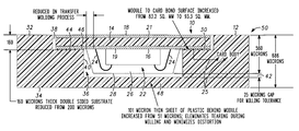
- Existing modules incorporate a 200 micron thick substrate and a 410 micron thick protective coating, giving a total module thickness of 610 microns.
- the total card thickness is typically specified at 762 microns ⁇ 76 microns, resulting in a card measuring 686 microns thick at the low end of the tolerance.
- the recess which receives the module is typically 635 microns deep, with a 25 micron tolerance for milling the recess in the card body.
- the bottom wall of the recess will have a thickness of 51 microns.
- such a thin bottom wall measuring about 51 microns increases distortion during the hot melt bonding used to secure the module to the card body.
- such a thin bottom wall frequently tears during milling when forming the recess in the card body.
- the glob topping process requires that a dam be dispensed around the die prior to application of the protective coating.
- the dam occupies a significant amount of surface area on the surface of the substrate, and thus less surface area is available for bonding the module to the card body.
- the available surface area is typically limited to about 83.2 square millimeters, which may not be sufficient to optimize the strength of the bond and which ultimately may lead to long term field reliability problems.
- Attempts have been made to employ thinner, metal rings as dams around the die in order to increase the available bonding area, but in practice such metal rings place the antenna pads too close to the metal rings, requiring much tighter tolerances which raises production costs.
- FIG. 1 is a schematic cross-sectional view of a dual mode module constructed in accordance with the teachings of a first preferred embodiment of the present invention and shown assembled in a card;
- FIG. 2 is a schematic cross-sectional view of a dual mode module constructed in accordance with the teachings of a second preferred embodiment of the present invention and shown assembled in a card;
- FIG. 3 is a schematic cross-sectional view of a prior art dual mode module
- FIG. 4 is a schematic cross-sectional view of the prior art dual mode module of FIG. 3 shown assembled in a card.
- FIG. 1 illustrates a dual mode smart card module assembled in accordance with the teachings of a first preferred embodiment of the present invention and which is referred to by the reference numeral 10 .
- the dual mode module 10 is adapted to enable both contacted and contactless smart card applications, which applications are known to those of skill in the art.
- the dual mode module 10 is shown installed in a card body or card 12 .
- the module 10 includes a double-sided substrate 14 having a lower side 16 and an upper side 18 . Each of the sides 16 , 18 has deposited thereon a metallic layer 19 , 21 , respectively.
- the substrate 14 has total thickness of one hundred sixty (160) microns, inclusive of the thickness of the metallic layers 19 , 21 , each of which measures thirty five (35) microns.
- the substrate 14 having the above-described dimensions is commercially available from a wide variety of sources.
- An integrated circuit (IC) wafer or die 22 is coupled to the metallic layer 19 of the lower side 16 , preferably by a plurality of wire bonds 24 .
- the die 22 may measure about 4.8 mm by about 5.2 mm, giving a total area of about 24 mm 2 .
- An antenna 25 of the type commonly employed in the art, such as a two turn wire antenna within the card body, is provided which enable the contactless application.
- the die 22 is preferably an EEPROM or an ASIC chip.
- a protective coating 26 covers the die 22 .
- the protective coating 26 is preferably an epoxy material, such as is commonly used in the semiconductor industry.
- the thickness of the protective coating 26 measures about four hundred (400) microns (i.e., the distance from the lower side 16 of the substrate 14 to a lower extent 28 of the protective coating 26 ). Accordingly, the module 10 will have a thickness of about 560 microns.
- a portion of the lower side 16 which remains uncovered by the protective coating 26 defines a bonding area 30 , which preferably measures about ninety three (93) square millimeters.
- the card 12 is generally rectangular in shape as would be known to those of skill in the art and is preferably manufactured of plastic such as PVC, ABS, PC, PET, or other suitable materials.
- the card 12 includes an upper face 32 and a lower face 34 .
- the card 12 also includes a cavity or recess 36 which includes an upper portion 38 sized to receive therein the substrate 14 and further includes a lower portion 40 sized to receive therein the die 22 including the full thickness of the protective coating 26 .
- a gap 42 is provided, preferably measuring twenty five (25) microns, for purposes of tolerance.
- the upper portion 38 of the recess 36 includes a ledge 44 , such that the bonding area 30 of the module 10 and card 12 meet at an interface 46 generally defined by the ledge 44 .
- the lower portion 40 of the recess 36 is bounded by a bottom layer or wall 48 , which preferably has a thickness of about one hundred and one (101) microns.
- both the upper portion 38 and the lower portion 40 of the recess 36 are formed in a known manner, such as by milling. With the module 10 secured in the card 12 as shown, the resulting dual mode smart card 50 will have a total thickness of about 686 microns.
- the card thickness is typically specified at 762 microns, ⁇ 76 microns, giving a lower limit of 686 microns. It will also be understood that when at this lower limit, the thickness of the bottom wall 48 becomes very important for two reasons. First, the bottom wall 48 , which has a minimum thickness that is thicker than the fifty one (51) micron minimum thickness found on prior art cards, is less susceptible to distortion in the presence of heat. Second, such a thicker bottom wall is less prone to tearing during the milling process used to create the recess 36 .
- the module 10 is assembled as follows.
- the die 22 is mounted adjacent the lower side 16 of the substrate 14 using conventional methods, the die 22 is glued or bonded in place, preferably using Tessa 8410 hot melt glue tape.
- the die 22 is operatively coupled to the conductive layer 21 on the lower side 16 of the substrate 14 .
- the antenna leads 25 are also connected to the die 22 in a known manner.
- the protective coating 26 is then formed by applying a sealed mold cavity, such as a hardened steel mold cavity (not shown) commonly employed for such purposes, around the die 22 .
- a sealed mold cavity such as a hardened steel mold cavity (not shown) commonly employed for such purposes.
- Molten epoxy is injected under pressure into the mold cavity in a conventional manner and allowed to cure.
- the mold cavity (not shown) is sized so that the resulting protective coating 26 is proportioned so that the bonding area 30 defined on the lower side 16 of the substrate 14 and surrounding the die/coating arrangement measures about ninety three (93) square millimeters.
- the card 12 is prepared by milling the upper portion 38 and the lower portion 40 of the recess 36 .
- the upper portion 38 must have a length and width sufficient to accept the corresponding length and width of the substrate 14 , and further must be deep enough to accommodate the thickness of the substrate (i.e., at least one hundred and sixty (160) microns). Further, the ledge 44 must have an area sufficient to receive thereon the full extent of the bonding area 30 along the interface 46 between the module 10 and the card 12 . After the recess 36 has been milled, the bottom wall 48 will have a thickness of about 101 microns, after allowing for a twenty five (25) micron tolerance at the gap 42 .
- the module 10 is secured to the card 12 , preferably by using the hot melt glue bonding which is well known in the art.
- the module 10 and the card 12 are secured along the interface 46 , such that the bonding area 30 has a total surface area of about ninety three (93) square millimeters.
- a dual mode smart card module assembled in accordance with the teachings of a second preferred embodiment of the present invention is referred to by the reference numeral 110 and is adapted to enable both contacted and contactless smart card applications.
- the dual mode module 110 is shown installed in a card 112 .
- the module 110 includes a double-sided substrate 114 having a lower side 116 and an upper side 118 . Each of the sides 116 , 118 has deposited thereon a metallic layer 119 , 121 , respectively.
- the substrate 114 has total thickness of one hundred twenty five (125) microns, inclusive of the thickness of the metallic layers 119 , 121 , each of which measures seventeen and one half (17.5) microns.
- a die 22 is operatively coupled to the metallic layer 119 of the lower side 116 by a plurality of wedge to wedge wire bonds 124 .
- a plurality of antennas 120 are provided which enable the contactless application.
- a protective coating 126 of an epoxy material covers the die 122 .
- the thickness of the protective coating 126 measures about three hundred seventy five (375) microns (i.e., the distance from the lower side 116 of the substrate 114 to a lower extent 128 of the protective coating 126 ). Accordingly, the module 110 will have a thickness of about five hundred (500) microns.
- a portion of the lower side 116 which remains uncovered by the protective coating 126 defines a bonding area 130 , which preferably measures about ninety three (93) square millimeters.
- the card 112 includes an upper face 132 and a lower face 134 .
- the card 112 also includes a cavity or recess 136 which includes an upper portion 138 sized to receive therein the substrate 114 and further includes a lower portion 140 sized to receive therein the die 122 including the full thickness of the protective coating 126 .
- a gap 142 is provided, preferably measuring twenty five (25) microns, for purposes of tolerance.
- the upper portion 138 of the recess 136 includes a ledge 144 , such that the bonding area 130 of the module 110 and card 112 meet at an interface 146 generally defined by the ledge 144 .
- the lower portion 140 of the recess 136 is bounded by a bottom layer or wall 148 , which preferably has a minimum thickness of about one hundred and sixty one (161) microns.
- both the upper portion 138 and the lower portion 140 of the recess 136 are formed in a known manner, such as by milling.
- the resulting dual mode smart card 150 will have a minimum total thickness of about six hundred eight six (686) microns.
Abstract
Description
Claims (32)
Priority Applications (2)
| Application Number | Priority Date | Filing Date | Title |
|---|---|---|---|
| US09/564,884 US6492717B1 (en) | 1999-08-03 | 2000-05-04 | Smart card module and method of assembling the same |
| US10/270,814 US6709889B2 (en) | 1999-08-03 | 2002-10-15 | Smart card module and method of assembling the same |
Applications Claiming Priority (2)
| Application Number | Priority Date | Filing Date | Title |
|---|---|---|---|
| US14692599P | 1999-08-03 | 1999-08-03 | |
| US09/564,884 US6492717B1 (en) | 1999-08-03 | 2000-05-04 | Smart card module and method of assembling the same |
Related Child Applications (1)
| Application Number | Title | Priority Date | Filing Date |
|---|---|---|---|
| US10/270,814 Division US6709889B2 (en) | 1999-08-03 | 2002-10-15 | Smart card module and method of assembling the same |
Publications (1)
| Publication Number | Publication Date |
|---|---|
| US6492717B1 true US6492717B1 (en) | 2002-12-10 |
Family
ID=26844419
Family Applications (2)
| Application Number | Title | Priority Date | Filing Date |
|---|---|---|---|
| US09/564,884 Expired - Fee Related US6492717B1 (en) | 1999-08-03 | 2000-05-04 | Smart card module and method of assembling the same |
| US10/270,814 Expired - Fee Related US6709889B2 (en) | 1999-08-03 | 2002-10-15 | Smart card module and method of assembling the same |
Family Applications After (1)
| Application Number | Title | Priority Date | Filing Date |
|---|---|---|---|
| US10/270,814 Expired - Fee Related US6709889B2 (en) | 1999-08-03 | 2002-10-15 | Smart card module and method of assembling the same |
Country Status (1)
| Country | Link |
|---|---|
| US (2) | US6492717B1 (en) |
Cited By (26)
| Publication number | Priority date | Publication date | Assignee | Title |
|---|---|---|---|---|
| US20030107138A1 (en) * | 2001-12-08 | 2003-06-12 | Micron Technology, Inc. | Die package |
| US20040084538A1 (en) * | 2000-01-25 | 2004-05-06 | Hitachi, Ltd. | IC card |
| US20040154161A1 (en) * | 2003-02-07 | 2004-08-12 | Hallys Corporation | Random-period chip transfer apparatus |
| US20040159709A1 (en) * | 2002-02-12 | 2004-08-19 | Eiji Ohta | IC card |
| US20040217178A1 (en) * | 2003-01-03 | 2004-11-04 | Ellen Lasch | Metal-containing transaction card and method of making the same |
| US6838758B1 (en) * | 2000-05-10 | 2005-01-04 | Advanced Micro Devices, Inc. | Package and method for making an underfilled integrated circuit |
| US6931234B1 (en) * | 1999-07-30 | 2005-08-16 | Nec Electronics Corporation | Data processing device and method of controlling operation of data processing device |
| US20060076662A1 (en) * | 2004-10-07 | 2006-04-13 | Cheng-Hsien Kuo | Memory card structure and manufacturing method thereof |
| US20060102729A1 (en) * | 2003-01-03 | 2006-05-18 | Priscilla Gandel | Metal-containing transaction card and method of making the same |
| US7193161B1 (en) * | 2006-02-15 | 2007-03-20 | Sandisk Corporation | SiP module with a single sided lid |
| US20070177359A1 (en) * | 2006-01-31 | 2007-08-02 | Cryovac, Inc. | Electronic device having improved electrical connection |
| US20070263368A1 (en) * | 2004-11-03 | 2007-11-15 | Gemplus | Device Comprising a Non-Detachable Electronic Device |
| US20080053617A1 (en) * | 2004-12-03 | 2008-03-06 | Hallys Corporation | Interposer Bonding Device |
| US20080314995A1 (en) * | 2003-01-03 | 2008-12-25 | American Express Travel Related Services Company, Inc. | Metal-containing transaction card and method of making same |
| US20090166431A1 (en) * | 2005-04-18 | 2009-07-02 | Hallys Corporation | Electronic component and manufacturing method thereof |
| US20090217515A1 (en) * | 2004-12-03 | 2009-09-03 | Hallys Corporation | Electronic component production method and electronic component production equipment |
| US7702538B2 (en) | 2000-08-01 | 2010-04-20 | Jpmorgan Chase Bank, N.A. | System and method for transponder-enabled account transactions |
| US20100176195A1 (en) * | 2006-08-22 | 2010-07-15 | Yoshinori Kubota | Discernment card and a discernment card business system using the discernment card |
| USD635186S1 (en) | 2008-06-30 | 2011-03-29 | Jpmorgan Chase Bank, N.A. | Metal transaction device |
| USD636020S1 (en) | 2008-07-17 | 2011-04-12 | Jpmorgan Chase Bank, N.A. | Eco-friendly transaction device |
| US8025086B2 (en) | 2005-04-06 | 2011-09-27 | Hallys Corporation | Electronic component manufacturing apparatus |
| US8033457B2 (en) | 2003-01-03 | 2011-10-11 | American Express Travel Related Services Company, Inc. | Metal-containing transaction card and method of making the same |
| US9305292B1 (en) | 2008-07-03 | 2016-04-05 | Jpmorgan Chase Bank, N.A. | Systems and methods for providing an adaptable transponder device |
| US20170293833A1 (en) * | 2016-04-12 | 2017-10-12 | Infineon Technologies Ag | Smart card and method for producing a smart card |
| US10607125B2 (en) | 2015-02-06 | 2020-03-31 | American Express Travel Related Services Company, Inc. | Method of making ceramic-containing transaction cards |
| US11088087B2 (en) * | 2018-07-25 | 2021-08-10 | Stmicroelectronics, Inc. | Micro module with a support structure |
Families Citing this family (19)
| Publication number | Priority date | Publication date | Assignee | Title |
|---|---|---|---|---|
| US6951596B2 (en) | 2002-01-18 | 2005-10-04 | Avery Dennison Corporation | RFID label technique |
| WO2002062588A1 (en) * | 2001-02-02 | 2002-08-15 | Hitachi, Ltd | Electronic device and method of manufacturing the same |
| JP2003346109A (en) * | 2002-05-22 | 2003-12-05 | Toshiba Corp | Ic card and semiconductor integrated circuit device package |
| US7500307B2 (en) * | 2004-09-22 | 2009-03-10 | Avery Dennison Corporation | High-speed RFID circuit placement method |
| US7623034B2 (en) * | 2005-04-25 | 2009-11-24 | Avery Dennison Corporation | High-speed RFID circuit placement method and device |
| US7555826B2 (en) | 2005-12-22 | 2009-07-07 | Avery Dennison Corporation | Method of manufacturing RFID devices |
| US7847380B2 (en) * | 2007-09-20 | 2010-12-07 | Samsung Electronics Co., Ltd. | Tape substrate and semiconductor module for smart card, method of fabricating the same, and smart card |
| US20090091424A1 (en) * | 2007-10-05 | 2009-04-09 | Manfred Rietzler | Transponder inlay for a personal document and method of manufacturing same |
| US8072764B2 (en) * | 2009-03-09 | 2011-12-06 | Apple Inc. | Multi-part substrate assemblies for low profile portable electronic devices |
| DE102014108626B4 (en) | 2014-06-18 | 2021-10-28 | Morpho Cards Gmbh | Manufacturing process for a laser-personalized chip card |
| CN108475344A (en) | 2015-08-14 | 2018-08-31 | 第资本服务有限责任公司 | Two-piece type transaction card structure |
| US11618191B2 (en) | 2016-07-27 | 2023-04-04 | Composecure, Llc | DI metal transaction devices and processes for the manufacture thereof |
| US10977540B2 (en) | 2016-07-27 | 2021-04-13 | Composecure, Llc | RFID device |
| US10762412B2 (en) | 2018-01-30 | 2020-09-01 | Composecure, Llc | DI capacitive embedded metal card |
| DK3491584T3 (en) | 2016-07-27 | 2022-10-17 | Composecure Llc | Molded electronic components for transaction cards and methods of making the same |
| CA3075405A1 (en) | 2017-09-07 | 2019-03-14 | Composecure, Llc | Transaction card with embedded electronic components and process for manufacture |
| US11151437B2 (en) | 2017-09-07 | 2021-10-19 | Composecure, Llc | Metal, ceramic, or ceramic-coated transaction card with window or window pattern and optional backlighting |
| WO2019079007A1 (en) | 2017-10-18 | 2019-04-25 | Composecure, Llc | Metal, ceramic, or ceramic-coated transaction card with window or window pattern and optional backlighting |
| USD948613S1 (en) | 2020-04-27 | 2022-04-12 | Composecure, Llc | Layer of a transaction card |
Citations (7)
| Publication number | Priority date | Publication date | Assignee | Title |
|---|---|---|---|---|
| US4625102A (en) * | 1983-06-09 | 1986-11-25 | Flonic | Memory card manufacturing method and cards thus obtained |
| US5378857A (en) | 1993-01-15 | 1995-01-03 | Advanced Interconnection Technology, Inc. | Directly bondable termination for a fixed discrete wire |
| US5519201A (en) | 1994-04-29 | 1996-05-21 | Us3, Inc. | Electrical interconnection for structure including electronic and/or electromagnetic devices |
| US6028774A (en) * | 1997-06-18 | 2000-02-22 | Samsung Electronics Co., Ltd. | Base cards and IC cards using the same |
| US6054774A (en) * | 1994-03-22 | 2000-04-25 | Kabushiki Kaisha Toshiba | Thin type semiconductor package |
| US6191366B1 (en) * | 1994-07-21 | 2001-02-20 | Hitachi Maxell, Ltd. | Board for IC card having component mounting recess |
| US6288905B1 (en) * | 1999-04-15 | 2001-09-11 | Amerasia International Technology Inc. | Contact module, as for a smart card, and method for making same |
-
2000
- 2000-05-04 US US09/564,884 patent/US6492717B1/en not_active Expired - Fee Related
-
2002
- 2002-10-15 US US10/270,814 patent/US6709889B2/en not_active Expired - Fee Related
Patent Citations (7)
| Publication number | Priority date | Publication date | Assignee | Title |
|---|---|---|---|---|
| US4625102A (en) * | 1983-06-09 | 1986-11-25 | Flonic | Memory card manufacturing method and cards thus obtained |
| US5378857A (en) | 1993-01-15 | 1995-01-03 | Advanced Interconnection Technology, Inc. | Directly bondable termination for a fixed discrete wire |
| US6054774A (en) * | 1994-03-22 | 2000-04-25 | Kabushiki Kaisha Toshiba | Thin type semiconductor package |
| US5519201A (en) | 1994-04-29 | 1996-05-21 | Us3, Inc. | Electrical interconnection for structure including electronic and/or electromagnetic devices |
| US6191366B1 (en) * | 1994-07-21 | 2001-02-20 | Hitachi Maxell, Ltd. | Board for IC card having component mounting recess |
| US6028774A (en) * | 1997-06-18 | 2000-02-22 | Samsung Electronics Co., Ltd. | Base cards and IC cards using the same |
| US6288905B1 (en) * | 1999-04-15 | 2001-09-11 | Amerasia International Technology Inc. | Contact module, as for a smart card, and method for making same |
Cited By (64)
| Publication number | Priority date | Publication date | Assignee | Title |
|---|---|---|---|---|
| US6931234B1 (en) * | 1999-07-30 | 2005-08-16 | Nec Electronics Corporation | Data processing device and method of controlling operation of data processing device |
| US20060157572A1 (en) * | 2000-01-25 | 2006-07-20 | Renesas Technology Corp. | IC card |
| US20040084538A1 (en) * | 2000-01-25 | 2004-05-06 | Hitachi, Ltd. | IC card |
| US7048197B2 (en) | 2000-01-25 | 2006-05-23 | Renesas Technology Corp. | IC card |
| US7552876B2 (en) | 2000-01-25 | 2009-06-30 | Renesas Technology Corp. | IC card |
| US20050090128A1 (en) * | 2000-01-25 | 2005-04-28 | Hitachi, Ltd. | IC card |
| US20050090129A1 (en) * | 2000-01-25 | 2005-04-28 | Hitachi, Ltd. | IC card |
| US20080257968A1 (en) * | 2000-01-25 | 2008-10-23 | Hirotaka Nishizawa | Ic card |
| US20060157573A1 (en) * | 2000-01-25 | 2006-07-20 | Renesas Technology Corp. | IC card |
| US7234644B2 (en) | 2000-01-25 | 2007-06-26 | Renesas Technology Corp. | IC card |
| US7303138B2 (en) | 2000-01-25 | 2007-12-04 | Renesas Technology Corp. | Integrated circuit card having staggered sequences of connector terminals |
| US7055757B2 (en) | 2000-01-25 | 2006-06-06 | Renesas Technology Corp. | IC card |
| US6838758B1 (en) * | 2000-05-10 | 2005-01-04 | Advanced Micro Devices, Inc. | Package and method for making an underfilled integrated circuit |
| US7702538B2 (en) | 2000-08-01 | 2010-04-20 | Jpmorgan Chase Bank, N.A. | System and method for transponder-enabled account transactions |
| US8781904B2 (en) | 2000-08-01 | 2014-07-15 | Jpmorgan Chase Bank, N.A. | System and method for transponder-enabled account transactions |
| US8781905B2 (en) | 2000-08-01 | 2014-07-15 | Jpmorgan Chase Bank, N.A. | System and method for transponder-enabled account transactions |
| US6919645B2 (en) | 2001-12-08 | 2005-07-19 | Micron Technology, Inc. | Die package |
| US20040164410A1 (en) * | 2001-12-08 | 2004-08-26 | Micron Technology, Inc. | Die package |
| US7489028B2 (en) * | 2001-12-08 | 2009-02-10 | Micron Technology, Inc. | Die package |
| US20050253226A1 (en) * | 2001-12-08 | 2005-11-17 | Micron Technology, Inc. | Die package |
| US20030107138A1 (en) * | 2001-12-08 | 2003-06-12 | Micron Technology, Inc. | Die package |
| US6825572B2 (en) * | 2001-12-08 | 2004-11-30 | Micron Technology, Inc. | Die package |
| US20040159709A1 (en) * | 2002-02-12 | 2004-08-19 | Eiji Ohta | IC card |
| US7377446B2 (en) * | 2002-12-02 | 2008-05-27 | Sony Corporation | IC card |
| US7494057B2 (en) | 2003-01-03 | 2009-02-24 | American Express Travel Related Services Company, Inc. | Metal-containing transaction card and method of making the same |
| US8033457B2 (en) | 2003-01-03 | 2011-10-11 | American Express Travel Related Services Company, Inc. | Metal-containing transaction card and method of making the same |
| US20040217178A1 (en) * | 2003-01-03 | 2004-11-04 | Ellen Lasch | Metal-containing transaction card and method of making the same |
| US8523062B2 (en) | 2003-01-03 | 2013-09-03 | American Express Travel Related Services Company, Inc. | Metal-containing transaction card and method of making the same |
| US8360312B2 (en) | 2003-01-03 | 2013-01-29 | American Express Travel Releated Services Company, Inc. | Metal-containing transaction card and method of making the same |
| US20070170264A1 (en) * | 2003-01-03 | 2007-07-26 | Ellen Lasch | Metal-containing transaction card and method of making the same |
| US20080314995A1 (en) * | 2003-01-03 | 2008-12-25 | American Express Travel Related Services Company, Inc. | Metal-containing transaction card and method of making same |
| US8079514B2 (en) | 2003-01-03 | 2011-12-20 | American Express Travel Related Services Company, Inc. | Metal-containing transaction card and method of making the same |
| US20110226858A1 (en) * | 2003-01-03 | 2011-09-22 | American Express Travel Related Services Company, Inc. | Metal-containing transaction card and method of making the same |
| US7530491B2 (en) | 2003-01-03 | 2009-05-12 | American Express Travel Related Services Company, Inc. | Metal-containing transaction card and method of making the same |
| US7971786B2 (en) | 2003-01-03 | 2011-07-05 | American Express Travel Related Services Company, Inc. | Metal-containing transaction card and method of making the same |
| US20060102729A1 (en) * | 2003-01-03 | 2006-05-18 | Priscilla Gandel | Metal-containing transaction card and method of making the same |
| US7823777B2 (en) | 2003-01-03 | 2010-11-02 | American Express Travel Related Services Company, Inc. | Metal-containing transaction card and method of making same |
| US7819310B2 (en) | 2003-01-03 | 2010-10-26 | American Express Travel Related Services Company Inc. | Metal-containing transaction card and method of making the same |
| US7588184B2 (en) * | 2003-01-03 | 2009-09-15 | American Express Travel Related Services Company, Inc. | Metal-containing transaction card and method of making the same |
| US7278203B2 (en) | 2003-02-07 | 2007-10-09 | Hallys Corporation | Random-period chip transfer apparatus |
| US20040154161A1 (en) * | 2003-02-07 | 2004-08-12 | Hallys Corporation | Random-period chip transfer apparatus |
| US7193304B2 (en) * | 2004-10-07 | 2007-03-20 | Advanced Flash Memory Card Technology Co., Ltd. | Memory card structure |
| US20060076662A1 (en) * | 2004-10-07 | 2006-04-13 | Cheng-Hsien Kuo | Memory card structure and manufacturing method thereof |
| US20070263368A1 (en) * | 2004-11-03 | 2007-11-15 | Gemplus | Device Comprising a Non-Detachable Electronic Device |
| US7578053B2 (en) | 2004-12-03 | 2009-08-25 | Hallys Corporation | Interposer bonding device |
| US20080053617A1 (en) * | 2004-12-03 | 2008-03-06 | Hallys Corporation | Interposer Bonding Device |
| US20090217515A1 (en) * | 2004-12-03 | 2009-09-03 | Hallys Corporation | Electronic component production method and electronic component production equipment |
| US8025086B2 (en) | 2005-04-06 | 2011-09-27 | Hallys Corporation | Electronic component manufacturing apparatus |
| US20090166431A1 (en) * | 2005-04-18 | 2009-07-02 | Hallys Corporation | Electronic component and manufacturing method thereof |
| US7551448B2 (en) | 2006-01-31 | 2009-06-23 | Cryovac, Inc. | Electronic device having improved electrical connection |
| US20070177359A1 (en) * | 2006-01-31 | 2007-08-02 | Cryovac, Inc. | Electronic device having improved electrical connection |
| US7193161B1 (en) * | 2006-02-15 | 2007-03-20 | Sandisk Corporation | SiP module with a single sided lid |
| US20100176195A1 (en) * | 2006-08-22 | 2010-07-15 | Yoshinori Kubota | Discernment card and a discernment card business system using the discernment card |
| US7975913B2 (en) | 2006-08-22 | 2011-07-12 | Rynne Group, Llc | Discernment card and a discernment card business system using the discernment card |
| USD643062S1 (en) | 2008-06-30 | 2011-08-09 | Jpmorgan Chase Bank, N.A. | Metal transaction device |
| USD635186S1 (en) | 2008-06-30 | 2011-03-29 | Jpmorgan Chase Bank, N.A. | Metal transaction device |
| US9305292B1 (en) | 2008-07-03 | 2016-04-05 | Jpmorgan Chase Bank, N.A. | Systems and methods for providing an adaptable transponder device |
| USD636020S1 (en) | 2008-07-17 | 2011-04-12 | Jpmorgan Chase Bank, N.A. | Eco-friendly transaction device |
| USD636021S1 (en) | 2008-07-17 | 2011-04-12 | Jpmorgan Chase Bank, N.A. | Eco-friendly transaction device |
| US10607125B2 (en) | 2015-02-06 | 2020-03-31 | American Express Travel Related Services Company, Inc. | Method of making ceramic-containing transaction cards |
| US11227201B1 (en) | 2015-02-06 | 2022-01-18 | American Express Travel Related Services Company, Inc | Ceramic transaction cards |
| US11915075B1 (en) | 2015-02-06 | 2024-02-27 | American Express Travel Related Services Company, Inc. | Ceramic transaction cards |
| US20170293833A1 (en) * | 2016-04-12 | 2017-10-12 | Infineon Technologies Ag | Smart card and method for producing a smart card |
| US11088087B2 (en) * | 2018-07-25 | 2021-08-10 | Stmicroelectronics, Inc. | Micro module with a support structure |
Also Published As
| Publication number | Publication date |
|---|---|
| US20030102541A1 (en) | 2003-06-05 |
| US6709889B2 (en) | 2004-03-23 |
Similar Documents
| Publication | Publication Date | Title |
|---|---|---|
| US6492717B1 (en) | Smart card module and method of assembling the same | |
| US5539251A (en) | Tie bar over chip lead frame design | |
| US5055913A (en) | Terminal arrangement for integrated circuit device | |
| US5545922A (en) | Dual sided integrated circuit chip package with offset wire bonds and support block cavities | |
| US5596225A (en) | Leadframe for an integrated circuit package which electrically interconnects multiple integrated circuit die | |
| KR100514023B1 (en) | Semiconductor device | |
| JPS6249741B2 (en) | ||
| US20010028107A1 (en) | Semiconductor device and a method of manufacturing the same | |
| US5898212A (en) | Lead frame and semiconductor package | |
| CN104303288A (en) | Fingerprint sensor package and method for manufacturing same | |
| US6002181A (en) | Structure of resin molded type semiconductor device with embedded thermal dissipator | |
| US20070170564A1 (en) | Chip card module | |
| US20030057536A1 (en) | Non-contact type IC card | |
| US6913951B2 (en) | Method of making a lead-on-chip device | |
| JPH0972804A (en) | Semiconductor pressure sensor | |
| US6166431A (en) | Semiconductor device with a thickness of 1 MM or less | |
| US6211573B1 (en) | Semiconductor device with an improved lead-chip adhesion structure and lead frame to be used therefor | |
| JPH08324166A (en) | Module for ic card and the card | |
| KR100262733B1 (en) | Chip On Board(COB) Package and Printed Circuit Board(PCB) thereof | |
| JPH0719859B2 (en) | Method for manufacturing IC card module | |
| JP2552887Y2 (en) | Insulator-coated electronic components | |
| US20120248589A1 (en) | Lead frame with coined inner leads | |
| KR940008329B1 (en) | Semiconductor package using inter connect lead and manufacturing method thereof | |
| US4918512A (en) | Semiconductor package having an outwardly arced die cavity | |
| JPH02251165A (en) | Resin seal type semiconductor device |
Legal Events
| Date | Code | Title | Description |
|---|---|---|---|
| AS | Assignment |
Owner name: MOTOROLA, INC., ILLINOIS Free format text: ASSIGNMENT OF ASSIGNORS INTEREST;ASSIGNORS:GORE, KIRON P.;HAAS, KEVIN;REEL/FRAME:010800/0579;SIGNING DATES FROM 20000503 TO 20000504 |
|
| CC | Certificate of correction | ||
| FPAY | Fee payment |
Year of fee payment: 4 |
|
| FPAY | Fee payment |
Year of fee payment: 8 |
|
| AS | Assignment |
Owner name: MOTOROLA SOLUTIONS, INC., ILLINOIS Free format text: CHANGE OF NAME;ASSIGNOR:MOTOROLA, INC;REEL/FRAME:026081/0001 Effective date: 20110104 |
|
| REMI | Maintenance fee reminder mailed | ||
| LAPS | Lapse for failure to pay maintenance fees | ||
| STCH | Information on status: patent discontinuation |
Free format text: PATENT EXPIRED DUE TO NONPAYMENT OF MAINTENANCE FEES UNDER 37 CFR 1.362 |
|
| FP | Lapsed due to failure to pay maintenance fee |
Effective date: 20141210 |