US6485873B1 - Electrophotographic photoconductor and electrophotographic apparatus - Google Patents

Electrophotographic photoconductor and electrophotographic apparatus Download PDF

Info

Publication number
US6485873B1
US6485873B1 US09/561,598 US56159800A US6485873B1 US 6485873 B1 US6485873 B1 US 6485873B1 US 56159800 A US56159800 A US 56159800A US 6485873 B1 US6485873 B1 US 6485873B1
Authority
US
United States
Prior art keywords
group
carbon atoms
alkyl
optionally substituted
atom
Prior art date
Legal status (The legal status is an assumption and is not a legal conclusion. Google has not performed a legal analysis and makes no representation as to the accuracy of the status listed.)
Expired - Fee Related
Application number
US09/561,598
Inventor
Kenichi Ohkura
Seizou Kitagawa
Masaru Takeuchi
Current Assignee (The listed assignees may be inaccurate. Google has not performed a legal analysis and makes no representation or warranty as to the accuracy of the list.)
Fuji Electric Co Ltd
Original Assignee
Fuji Electric Imaging Device Co Ltd
Priority date (The priority date is an assumption and is not a legal conclusion. Google has not performed a legal analysis and makes no representation as to the accuracy of the date listed.)
Filing date
Publication date
Application filed by Fuji Electric Imaging Device Co Ltd filed Critical Fuji Electric Imaging Device Co Ltd
Assigned to FUJI ELECTRIC IMAGING DEVICE CO., LTD. reassignment FUJI ELECTRIC IMAGING DEVICE CO., LTD. ASSIGNMENT OF ASSIGNORS INTEREST (SEE DOCUMENT FOR DETAILS). Assignors: KITAGAWA, SEIZOU, OHKURA, KENICHI, TAKEUCHI, MASARU
Application granted granted Critical
Publication of US6485873B1 publication Critical patent/US6485873B1/en
Assigned to FUJI ELECTRIC DEVICE TECHNOLOGY CO., LTD. reassignment FUJI ELECTRIC DEVICE TECHNOLOGY CO., LTD. ASSIGNMENT OF ASSIGNORS INTEREST (SEE DOCUMENT FOR DETAILS). Assignors: FUJI ELECTRIC HOLDINGS CO., LTD.
Assigned to FUJI ELECTRIC HOLDINGS CO., LTD. reassignment FUJI ELECTRIC HOLDINGS CO., LTD. CHANGE OF NAME (SEE DOCUMENT FOR DETAILS). Assignors: FUJI ELECTRIC CO., LTD.
Assigned to FUJI ELECTRIC SYSTEMS CO., LTD. reassignment FUJI ELECTRIC SYSTEMS CO., LTD. ASSIGNMENT OF ASSIGNORS INTEREST (SEE DOCUMENT FOR DETAILS). Assignors: FUJI ELECTRIC DEVICE TECHNOLOGY CO., LTD.
Anticipated expiration legal-status Critical
Expired - Fee Related legal-status Critical Current

Links

Images

Classifications

    • GPHYSICS
    • G03PHOTOGRAPHY; CINEMATOGRAPHY; ANALOGOUS TECHNIQUES USING WAVES OTHER THAN OPTICAL WAVES; ELECTROGRAPHY; HOLOGRAPHY
    • G03GELECTROGRAPHY; ELECTROPHOTOGRAPHY; MAGNETOGRAPHY
    • G03G5/00Recording members for original recording by exposure, e.g. to light, to heat, to electrons; Manufacture thereof; Selection of materials therefor
    • G03G5/02Charge-receiving layers
    • G03G5/04Photoconductive layers; Charge-generation layers or charge-transporting layers; Additives therefor; Binders therefor
    • G03G5/06Photoconductive layers; Charge-generation layers or charge-transporting layers; Additives therefor; Binders therefor characterised by the photoconductive material being organic
    • G03G5/0664Dyes
    • G03G5/0666Dyes containing a methine or polymethine group
    • G03G5/0672Dyes containing a methine or polymethine group containing two or more methine or polymethine groups
    • GPHYSICS
    • G03PHOTOGRAPHY; CINEMATOGRAPHY; ANALOGOUS TECHNIQUES USING WAVES OTHER THAN OPTICAL WAVES; ELECTROGRAPHY; HOLOGRAPHY
    • G03GELECTROGRAPHY; ELECTROPHOTOGRAPHY; MAGNETOGRAPHY
    • G03G5/00Recording members for original recording by exposure, e.g. to light, to heat, to electrons; Manufacture thereof; Selection of materials therefor
    • G03G5/02Charge-receiving layers
    • G03G5/04Photoconductive layers; Charge-generation layers or charge-transporting layers; Additives therefor; Binders therefor
    • G03G5/06Photoconductive layers; Charge-generation layers or charge-transporting layers; Additives therefor; Binders therefor characterised by the photoconductive material being organic
    • G03G5/0601Acyclic or carbocyclic compounds
    • G03G5/0605Carbocyclic compounds
    • GPHYSICS
    • G03PHOTOGRAPHY; CINEMATOGRAPHY; ANALOGOUS TECHNIQUES USING WAVES OTHER THAN OPTICAL WAVES; ELECTROGRAPHY; HOLOGRAPHY
    • G03GELECTROGRAPHY; ELECTROPHOTOGRAPHY; MAGNETOGRAPHY
    • G03G5/00Recording members for original recording by exposure, e.g. to light, to heat, to electrons; Manufacture thereof; Selection of materials therefor
    • G03G5/02Charge-receiving layers
    • G03G5/04Photoconductive layers; Charge-generation layers or charge-transporting layers; Additives therefor; Binders therefor
    • G03G5/06Photoconductive layers; Charge-generation layers or charge-transporting layers; Additives therefor; Binders therefor characterised by the photoconductive material being organic
    • G03G5/0601Acyclic or carbocyclic compounds
    • G03G5/0609Acyclic or carbocyclic compounds containing oxygen
    • GPHYSICS
    • G03PHOTOGRAPHY; CINEMATOGRAPHY; ANALOGOUS TECHNIQUES USING WAVES OTHER THAN OPTICAL WAVES; ELECTROGRAPHY; HOLOGRAPHY
    • G03GELECTROGRAPHY; ELECTROPHOTOGRAPHY; MAGNETOGRAPHY
    • G03G5/00Recording members for original recording by exposure, e.g. to light, to heat, to electrons; Manufacture thereof; Selection of materials therefor
    • G03G5/02Charge-receiving layers
    • G03G5/04Photoconductive layers; Charge-generation layers or charge-transporting layers; Additives therefor; Binders therefor
    • G03G5/06Photoconductive layers; Charge-generation layers or charge-transporting layers; Additives therefor; Binders therefor characterised by the photoconductive material being organic
    • G03G5/0601Acyclic or carbocyclic compounds
    • G03G5/0612Acyclic or carbocyclic compounds containing nitrogen
    • G03G5/0614Amines
    • G03G5/06142Amines arylamine
    • G03G5/06144Amines arylamine diamine
    • G03G5/061443Amines arylamine diamine benzidine
    • GPHYSICS
    • G03PHOTOGRAPHY; CINEMATOGRAPHY; ANALOGOUS TECHNIQUES USING WAVES OTHER THAN OPTICAL WAVES; ELECTROGRAPHY; HOLOGRAPHY
    • G03GELECTROGRAPHY; ELECTROPHOTOGRAPHY; MAGNETOGRAPHY
    • G03G5/00Recording members for original recording by exposure, e.g. to light, to heat, to electrons; Manufacture thereof; Selection of materials therefor
    • G03G5/02Charge-receiving layers
    • G03G5/04Photoconductive layers; Charge-generation layers or charge-transporting layers; Additives therefor; Binders therefor
    • G03G5/06Photoconductive layers; Charge-generation layers or charge-transporting layers; Additives therefor; Binders therefor characterised by the photoconductive material being organic
    • G03G5/0601Acyclic or carbocyclic compounds
    • G03G5/0612Acyclic or carbocyclic compounds containing nitrogen
    • G03G5/0614Amines
    • G03G5/06142Amines arylamine
    • G03G5/06145Amines arylamine triamine or greater
    • GPHYSICS
    • G03PHOTOGRAPHY; CINEMATOGRAPHY; ANALOGOUS TECHNIQUES USING WAVES OTHER THAN OPTICAL WAVES; ELECTROGRAPHY; HOLOGRAPHY
    • G03GELECTROGRAPHY; ELECTROPHOTOGRAPHY; MAGNETOGRAPHY
    • G03G5/00Recording members for original recording by exposure, e.g. to light, to heat, to electrons; Manufacture thereof; Selection of materials therefor
    • G03G5/02Charge-receiving layers
    • G03G5/04Photoconductive layers; Charge-generation layers or charge-transporting layers; Additives therefor; Binders therefor
    • G03G5/06Photoconductive layers; Charge-generation layers or charge-transporting layers; Additives therefor; Binders therefor characterised by the photoconductive material being organic
    • G03G5/0601Acyclic or carbocyclic compounds
    • G03G5/0612Acyclic or carbocyclic compounds containing nitrogen
    • G03G5/0614Amines
    • G03G5/06142Amines arylamine
    • G03G5/06147Amines arylamine alkenylarylamine
    • G03G5/061473Amines arylamine alkenylarylamine plural alkenyl groups linked directly to the same aryl group
    • GPHYSICS
    • G03PHOTOGRAPHY; CINEMATOGRAPHY; ANALOGOUS TECHNIQUES USING WAVES OTHER THAN OPTICAL WAVES; ELECTROGRAPHY; HOLOGRAPHY
    • G03GELECTROGRAPHY; ELECTROPHOTOGRAPHY; MAGNETOGRAPHY
    • G03G5/00Recording members for original recording by exposure, e.g. to light, to heat, to electrons; Manufacture thereof; Selection of materials therefor
    • G03G5/02Charge-receiving layers
    • G03G5/04Photoconductive layers; Charge-generation layers or charge-transporting layers; Additives therefor; Binders therefor
    • G03G5/06Photoconductive layers; Charge-generation layers or charge-transporting layers; Additives therefor; Binders therefor characterised by the photoconductive material being organic
    • G03G5/0601Acyclic or carbocyclic compounds
    • G03G5/0618Acyclic or carbocyclic compounds containing oxygen and nitrogen
    • GPHYSICS
    • G03PHOTOGRAPHY; CINEMATOGRAPHY; ANALOGOUS TECHNIQUES USING WAVES OTHER THAN OPTICAL WAVES; ELECTROGRAPHY; HOLOGRAPHY
    • G03GELECTROGRAPHY; ELECTROPHOTOGRAPHY; MAGNETOGRAPHY
    • G03G5/00Recording members for original recording by exposure, e.g. to light, to heat, to electrons; Manufacture thereof; Selection of materials therefor
    • G03G5/02Charge-receiving layers
    • G03G5/04Photoconductive layers; Charge-generation layers or charge-transporting layers; Additives therefor; Binders therefor
    • G03G5/06Photoconductive layers; Charge-generation layers or charge-transporting layers; Additives therefor; Binders therefor characterised by the photoconductive material being organic
    • G03G5/0601Acyclic or carbocyclic compounds
    • G03G5/062Acyclic or carbocyclic compounds containing non-metal elements other than hydrogen, halogen, oxygen or nitrogen
    • GPHYSICS
    • G03PHOTOGRAPHY; CINEMATOGRAPHY; ANALOGOUS TECHNIQUES USING WAVES OTHER THAN OPTICAL WAVES; ELECTROGRAPHY; HOLOGRAPHY
    • G03GELECTROGRAPHY; ELECTROPHOTOGRAPHY; MAGNETOGRAPHY
    • G03G5/00Recording members for original recording by exposure, e.g. to light, to heat, to electrons; Manufacture thereof; Selection of materials therefor
    • G03G5/02Charge-receiving layers
    • G03G5/04Photoconductive layers; Charge-generation layers or charge-transporting layers; Additives therefor; Binders therefor
    • G03G5/06Photoconductive layers; Charge-generation layers or charge-transporting layers; Additives therefor; Binders therefor characterised by the photoconductive material being organic
    • G03G5/0622Heterocyclic compounds
    • G03G5/0644Heterocyclic compounds containing two or more hetero rings
    • G03G5/0661Heterocyclic compounds containing two or more hetero rings in different ring systems, each system containing at least one hetero ring
    • GPHYSICS
    • G03PHOTOGRAPHY; CINEMATOGRAPHY; ANALOGOUS TECHNIQUES USING WAVES OTHER THAN OPTICAL WAVES; ELECTROGRAPHY; HOLOGRAPHY
    • G03GELECTROGRAPHY; ELECTROPHOTOGRAPHY; MAGNETOGRAPHY
    • G03G5/00Recording members for original recording by exposure, e.g. to light, to heat, to electrons; Manufacture thereof; Selection of materials therefor
    • G03G5/02Charge-receiving layers
    • G03G5/04Photoconductive layers; Charge-generation layers or charge-transporting layers; Additives therefor; Binders therefor
    • G03G5/06Photoconductive layers; Charge-generation layers or charge-transporting layers; Additives therefor; Binders therefor characterised by the photoconductive material being organic
    • G03G5/0664Dyes
    • G03G5/0666Dyes containing a methine or polymethine group
    • G03G5/0672Dyes containing a methine or polymethine group containing two or more methine or polymethine groups
    • G03G5/0674Dyes containing a methine or polymethine group containing two or more methine or polymethine groups containing hetero rings

Definitions

  • the present invention relates to electrophotographic photoconductors having improved electrical characteristics in a positive charging process.
  • the present invention further relates to electrophotographic apparatus using the aforementioned electrophotographic photoconductor.
  • a photosensitive layer of an organic electrophotographic photoconductor principally consists of a layer having organic photosensitive material dispersed in a resin material.
  • Many types of photosensitive layer structures have been proposed, including laminate structures and single-layer structures.
  • a laminate structure consists of a charge generation layer, containing a charge generation substance, dispersed in a resin, and a charge transport layer, containing charge transport substance, dispersed in a resin.
  • a single-layer structure consists of a single-layer containing both a charge generation substance and a charge transport substance dispersed in a resin.
  • a photosensitive layer In conventional functional-separated type photoconductor, a photosensitive layer consists of a charge transport layer and a charge generation layer. The charge transport layer is laminated on a charge generation layer.
  • This type of photoconductor is widely used because of its excellent photoconductor characteristics and durability.
  • the charge transport layer of the function-separated laminate type photoconductor generally uses a hole transport substance. Therefore, the type of photoconductor is utilized in a negative-charging process. Negative polar corona discharge in the negative-charging process is less stable and generates larger amount of ozone as compared to a positive polar corona discharge. This raises problems such as undesirable effects to the photoconductor and hazardous influence to the operation environment.
  • an organic electrophotographic photoconductor which can be used in a positive-charging process.
  • a positive-charging type photoconductor exhibiting high sensitivity is presently desired.
  • Numerous photosensitive layers of the positive-charging type photoconductor have been proposed.
  • a function-separated type photoconductor having a charge generation layer laminated on a hole transport layer has been proposed.
  • a function-separated type photoconductor having an electron transport layer laminated on a charge generation layer has also been proposed.
  • a single-layer type photoconductor having a charge generation substance and charge transport substance contained in the same layer has been proposed.
  • most of these conventional photoconductors are inferior in electrical characteristics, such as sensitivity, as compared to photosensitive layers of negative-charging function-separated photoconductors.
  • Biphenyl derivatives are used as a plasticizer for plastics.
  • Further applications of biphenyl derivatives, as a deactivating agent contemplating stability in repeated use by preventing dimerization or dissociation of certain charge transport substances have been proposed in Japanese Unexamined Patent Application Publications (KOKAI) Nos. H3-75754, H3-75755, and H3-75756.
  • biphenyl derivatives as an agent for increasing electrostatic force and van der Vaals' force contemplating high image density, is proposed in Japanese Unexamined Patent Application Publication (KOKAI) No. H5-273771.
  • an application containing the biphenyl derivative in a charge generating layer to improve adhesivity of the charge generating layer to a charge transport layer, an intermediate layer, or a substrate is proposed in Japanese Unexamined Patent Application Publication (KOKAI) No. H10-268532.
  • the present invention provides a biphenyl derivative included in a photosensitive layer of an electrophotographic photoconductor.
  • the electrophotographic photoconductor includes a single-layer photosensitive layer coated on a conductive substrate.
  • the photosensitive layer includes a resin binder, a charge generation substance, a hole transport substance, and an electron transport substance.
  • An electrophotographic apparatus using such an electrophotographic photoconductor has excellent electrical characteristics in a positive charging system and is stable in repeated use.
  • an electrophotographic photoconductor comprising: a conductive substrate; a single-layer photosensitive layer disposed on the conductive substrate; the single-layer photosensitive layer including a resin binder, a charge generation substance, a hole transport substance, and an electron transport substance; and the single-layer photosensitive layer contains a biphenyl derivative.
  • FIG. 1 is a schematic sectional view of an electrophotographic photoconductor according to the present invention.
  • the photosensitive layer includes a resin binder, a charge generating substance, a hole transport substance, and an electron transport substance acting as an acceptor compound.
  • the present invention is achieved based on this finding.
  • the present invention provides an electrophotographic photoconductor comprising a conductive substrate and a single-layer photosensitive layer disposed directly or through an undercoat layer on the substrate.
  • the photosensitive layer includes at least, a resin binder, a charge generating substance, a hole transport substance, and an electron transport substance, wherein the photosensitive layer contains a biphenyl derivative.
  • the biphenyl derivative has a structure represented by general formula (BP1).
  • R P1 is a hydrogen atom, an optionally substituted aryl group, an optionally substituted aralkyl group, or a cycloalkyl group.
  • Each of R P2 to R P10 is independently a hydrogen atom, a halogen atom, an alkyl group of 1 to 18 carbon atoms, an alkoxyl group of 1 to 18 carbon atoms, a hydroxyl group, an alkyl halide group, a cyano group, nitro group, or an alkyl-substituted amino group optionally forming a ring with a nitrogen atom.
  • the substituent in the formula (BP 1 ) is a halogen atom, an alkyl group of 1 to 6 carbon atoms, an alkoxyl group of 1 to 6 carbon atoms, a hydroxyl group, a cyano group, an amino group, a nitro group, or an alkyl halide group.
  • the biphenyl derivative is a compound selected from the group consisting of a biphenyl, o-terphenyl, m-terphenyl, p-terphenyl, p-benzylbiphenyl, and hydrogenated terphenyl.
  • An alkyl group may branched or straight chained.
  • At least one of the electron transport substances is selected from the acceptor compounds represented by the following general formulas (ET1) to (ET15).
  • each of R E1 to R E4 is independently a hydrogen atom, an alkyl group of 1 to 12 carbon atoms, an alkoxyl group of 1 to 12 carbon atoms, an optionally substituted aryl group, a cycloalkyl group, an optionally substituted aralkyl group, or an alkyl halide group.
  • the substituent in the formula (ET1) is a halogen atom, an alkyl group of 1 to 6 carbon atoms, an alkoxyl group of 1 to 6 carbon atoms, a hydroxyl group, a cyano group, an amino group, a nitro group, or an alkyl halide group.
  • each of R E5 to R E8 is independently a hydrogen atom, an alkyl group of 1 to 12 carbon atoms, an alkoxyl group of 1 to 12 carbon atoms, an optionally substituted aryl group, a cycloalkyl group, an optionally substituted aralkyl group, or an alkyl halide group.
  • the substituent in the formula (ET2) is a halogen atom, an alkyl group of 1 to 6 carbon atoms, an alkoxyl group of 1 to 6 carbon atoms, a hydroxyl group, a cyano group, an amino group, a nitro group, or an alkyl halide group.
  • each of R E9 to R E10 is independently a hydrogen atom, an alkyl group of 1 to 12 carbon atoms, an alkoxyl group of 1 to 12 carbon atoms, an optionally substituted aryl group, a cycloalkyl group, an optionally substituted aralkyl group, or an alkyl halide group.
  • the substituent in the formula (ET3) is a halogen atom, an alkyl group of 1 to 6 carbon atoms, an alkoxyl group of 1 to 6 carbon atoms, a hydroxyl group, a cyano group, an amino group, a nitro group, or an alkyl halide group.
  • each of R E11 and R E12 is independently a hydrogen atom, an alkyl group of 1 to 12 carbon atoms, an alkoxyl group of 1 to 12 carbon atoms, an optionally substituted aryl group, a cycloalkyl group, an optionally substituted aralkyl group, or an alkyl halide group.
  • Each of R E13 to R E17 is independently a hydrogen atom, a halogen atom, an alkyl group of 1 to 12 carbon atoms, an alkoxyl group of 1 to 12 carbon atoms, an optionally substituted aryl group, an optionally substituted aralkyl group, an optionally substituted phenoxy group, or an alkyl halide group, wherein two or more of the groups may bond one another to for a ring.
  • the substituent in the formula (ET4) is a halogen atom, an alkyl group of 1 to 6 carbon atoms, an alkoxyl group of 1 to 6 carbon atoms, a hydroxyl group, a cyano group, an amino group, a nitro group, or an alkyl halide group.
  • each of R E18 to R E21 is independently a hydrogen atom, an alkyl group of 1 to 12 carbon atoms, an alkoxyl group of 1 to 12 carbon atoms, an optionally substituted aryl group, a cycloalkyl group, an optionally substituted aralkyl group, or an alkyl halide group.
  • Each of R E22 and R E23 is independently a hydrogen atom, or an alkyl group of 1 to 12 carbon atoms.
  • Each of R E24 to R E31 is independently a hydrogen atom, a halogen atom, an alkyl group of 1 to 12 carbon atoms, an alkoxyl group of 1 to 12 carbon atoms, an optionally substituted aryl group, or an alkyl halide group.
  • the substituent in the formula (ET5) is a halogen atom, an alkyl group of 1 to 6 carbon atoms, an alkoxyl group of 1 to 6 carbon atoms, a hydroxyl group, a cyano group, an amino group, a nitro group, or an alkyl halide group.
  • each of R E32 to R E36 is independently a hydrogen atom, a halogen atom, a cyano group, a nitro group, an alkyl group of 1 to 12 carbon atoms, an alkoxyl group of 1 to 12 carbon atoms, an optionally substituted aryl group, an optionally substituted aralkyl group, an optionally substituted phenoxy group, or an alkyl halide group.
  • Each of R E37 to R E44 is a hydrogen atom or a nitro group, at least three of the R E37 to RS being nitro groups.
  • the substituent in the formula (ET6) is a halogen atom, an alkyl group of 1 to 6 carbon atoms, an alkoxyl group of 1 to 6 carbon atoms, a hydroxyl group, a cyano group, an amino group, a nitro group, or an alkyl halide group.
  • R E45 is an optionally substituted alkyl group or an optionally substituted aryl group.
  • R E46 is an optionally substituted alkyl group, an optionally substituted aryl group, or a group represented by the following formula (ET7a), in which R E47 is an optionally substituted alkyl group or an optionally substituted aryl group.
  • the substituent in the formula (ET7) and the formula (ET7a) is a halogen atom, an alkyl group of 1 to 6 carbon atoms, an alkoxyl group of 1 to 6 carbon atoms, a hydroxyl group, a cyano group, an amino group, a nitro group, or an alkyl halide group.
  • each of R E48 to R E60 is independently a hydrogen atom, an alkyl group of 1 to 6 carbon atoms, an alkoxyl group of 1 to 6 carbon atoms, an aryl group, an aralkyl group, a halogen atom, or an alkyl halide group.
  • each of R E61 to R E68 is independently a hydrogen atom, an alkyl group of 1 to 6 carbon atoms, an alkoxyl group of 1 to 6 carbon atoms, an aryl group, an aralkyl group, a halogen atom, or an alkyl halide group.
  • each of R E69 and R E70 is independently a cyano group or an alkoxycarbonyl group.
  • R E71 is a hydrogen atom, an alkyl group of 1 to 12 carbon atoms, or an optionally substituted aryl group.
  • R E72 to R E76 is independently a hydrogen atom, a halogen atom, an alkyl group of 1 to 12 carbon atoms, an alkoxyl group, an optionally substituted aryl group, an alkyl halide group, or alkyl-substituted amino group.
  • R E77 to R E79 is independently a hydrogen atom or an alkyl group of 1 to 12 carbon atoms.
  • R E80 and R E81 is independently a hydrogen atom, halogen atom, an alkyl group of 1 to 12 carbon atoms, or an optionally substituted aryl group.
  • X is a sulfur atom or an oxygen atom
  • n is 0 or 1.
  • the substituent in the formula (ET10) is a halogen atom, an alkyl group of 1 to 6 carbon atoms, an alkoxyl group of 1 to 6 carbon atoms, a hydroxyl group, a cyano group, an amino group, a nitro group, or an alkyl halide group.
  • each of R E82 to R E85 is independently a hydrogen atom or a halogen atom.
  • Each of R E86 and R E87 is independently a cyano group or an alkoxycarbonyl group.
  • Each of R E88 to R E92 is independently a hydrogen atom, a halogen atom, an alkyl group of 1 to 6 carbon atoms, a nitro group, or a cyano group.
  • each of R E93 to R E96 is independently a hydrogen atom or a halogen atom.
  • Each of R E97 and R E98 is independently a cyano group or an alkoxycarbonyl group.
  • Each of R E99 to R E103 is independently a hydrogen atom, a halogen atom, an alkyl group of 1 to 6 carbon atoms, a nitro group, or a cyano group.
  • At least one of the hole transport substances is a compound represented by the following general formulas (HT1) to (HT5).
  • each of R H1 -R H32 is independently a hydrogen atom, an alkyl group of 1 to 6 carbon atoms, or an alkoxyl group of 1 to 6 carbon atoms.
  • R H33 is a hydrogen atom or an alkyl group of 1 to 6 carbon atoms.
  • R H34 and R H35 is independently a hydrogen atom, an alkyl group of 1 to 6 carbon atoms, an alkoxyl group of 1 to 6 carbon atoms, or an optionally substituted aryl group, in which R H34 and R H35 may bond each other to form a ring, directly or through a carbon chain, an oxygen atom, or a sulfur atom.
  • Each of R H36 and R H37 is independently an alkyl group of 1 to 12 carbon atoms, an optionally substituted cycloalkyl group of 3 to 12 carbon atoms, an optionally substituted aryl group, or an optionally substituted aralkyl group.
  • Each of R H38 to R H41 is independently a hydrogen atom, an alkyl group of 1 to 6 carbon atoms, an alkoxyl group of 1 to 6 carbon atoms, or an optionally substituted aryl group. Two or more of the R H36 to R H41 may bond one another to form a ring, directly or through a carbon chain, an oxygen atom, or a sulfur atom.
  • m is 0 or 1.
  • the substituent in the formula (HT2) is a halogen atom, an alkyl group of 1 to 6 carbon atoms, an alkoxyl group of 1 to 6 carbon atoms, an optionally substituted aryl group, a hydroxyl group, a cyano group, an amino group, a nitro group, an alkyl halide group, or an alkyl-substituted amino group. Two or more of these substituent groups may bond one another to form a ring, directly or through a carbon chain, an oxygen atom, or a sulfur atom.
  • each of R H42 to R H60 is independently a hydrogen atom, a halogen atom, an alkyl group of 1 to 12 carbon atoms, an alkoxyl group of 1 to 12 carbon atoms, an alkyl-substituted amino group, or an optionally substituted aryl group, in which two or more of R H42 to R H60 may bond one another to form a ring, directly or through a carbon chain, an oxygen atom, or a sulfur atom.
  • the substituent in the formula (HT3) is a halogen atom, an alkyl group of 1 to 6 carbon atoms, an alkoxyl group of 1 to 6 carbon atoms, a hydroxyl group, a cyano group, an amino group, a nitro group, or an alkyl halide group, in which two or more of these substituent groups may bond one another to form a ring, directly or through a carbon chain, an oxygen atom, or a sulfur atom.
  • each of R H61 to R H88 is independently a hydrogen atom, a halogen atom, an aryl group, an alkyl group of 1 to 12 carbon atoms, an alkoxyl group of 1 to 12 carbon atoms or an optionally substituted aryl group.
  • the substituent in the formula (HT4) is a halogen atom, an alkyl group of 1 to 6 carbon atoms, or an alkoxyl group of 1 to 6 carbon atoms.
  • each of R H89 to R H92 is independently an alkyl group of 1 to 6 carbon atoms, or an optionally substituted aralkyl group.
  • Each of R H93 to R H102 is independently a hydrogen atom, a halogen atom, an alkyl group of 1 to 6 carbon atoms, or an alkoxyl group of 1 to 6 carbon atoms.
  • the substituent in the formula (HT5) is a halogen atom, an alkyl group of 1 to 6 carbon atoms, or an alkoxyl group of 1 to 6 carbon atoms.
  • At least one of the charge generation substances is an X-type metal-free phthalocyanine.
  • At least one of the resin binder is polycarbonate having a structural unit represented by the general formula (BD1) below as a principal repeating unit.
  • each of R B1 to R B8 is independently a hydrogen atom, an alkyl group of 1 to 6 carbon atoms, an optionally substituted aryl group, a cycloalkyl group, or an halogen atom.
  • Z is a group of atoms needed to form an optionally substituted carbon ring.
  • the substituent in the formula (BD1) is an alkyl group of 1 to 6 carbon atoms or a halogen atom.
  • the electrophotographic apparatus of the present invention is provided with the above-described electrophotographic photoconductor of the present invention.
  • the charging process of the electrophotographic apparatus of the present invention is performed by a positive-charging process.
  • FIG. 1 is a cross sectional view showing an electrophotographic photoconductor according to the present invention.
  • An undercoat layer 2 is coated on a conductive substrate 1 .
  • a photosensitive layer 3 and an optional protection layer 4 are then subsequently coated on conductive substrate 1 .
  • Undercoat layer 2 and protection layer 4 are provided as needed.
  • Photosensitive layer 3 of the present invention is preferably of a single-layer type, performing both a charge generation function and a charge transport function.
  • Conductive substrate 1 acting as a support for the other layers, functions as an electrode of the photoconductor.
  • Conductive substrate 1 may have a cylindrical shape, planar shape, or film-like shape, and may be formed of a metal, such as aluminum, stainless steel or nickel, or glass or resin that has been treated to be given a certain conductivity.
  • Undercoat layer 2 which may be formed of a layer containing a resin as a major component, or of an oxide film such as alumite, is provided as needed for the purposes of preventing unnecessary charges from injecting from conductive substrate 1 into photosensitive layer 3 .
  • Undercoat layer 2 also acts to cover defects on the surface of conductive substrate 1 , and improving the adhesivity of photosensitive layer 3 .
  • the binder resin of undercoat layer 2 is preferably selected from polycarbonate resin, polyester resin, polyvinylacetal resin, polyvinylbutyral resin, polyvinylalcohol resin, vinylchloride resin, vinylacetate resin, polyethylene, polypropylene, acrylic resin, polyurethane resin, epoxy resin, melamine resin, silicon resin, polyamide resin, polystyrene resin, polyacetal resin, polyarylate resin, polysulfone resin, and polymer of methacrylic acid ester, and copolymers of these resins, which may be used in suitable combination.
  • a mixture of resins of the same species but different molecular weight may also be used as a binder resin.
  • the binder resin may contain fine particles of a metal oxide, such as silicon oxide (silica), titanium oxide, zinc oxide, calcium oxide, aluminum oxide (alumina), or zirconium oxide, a metal sulfate, such as barium sulfate or calcium sulfate, or a metal nitride, such as silicon nitride or aluminum nitride.
  • a metal oxide such as silicon oxide (silica), titanium oxide, zinc oxide, calcium oxide, aluminum oxide (alumina), or zirconium oxide
  • a metal sulfate such as barium sulfate or calcium sulfate
  • a metal nitride such as silicon nitride or aluminum nitride.
  • the binder resin may contain an organic metal compound, a silane coupling agent, or a material formed of an organic metal compound and a silane coupling agent. The content of these additives may be set to a desired value within a range in which an undercoat layer can be actually formed.
  • Undercoat layer 2 which is formed of a resin as a major component, may contain a charge transport substance for the purpose to give charge transport ability or to suppress charge trapping.
  • the content of such charge transport substance is from about 0.1 to about 60 wt. %, preferably from about 5 to about 40 wt. % with respect to a solid component of undercoat layer 2 .
  • Undercoat layer 2 may further contain other known additives as needed, so far as the additives don't much deteriorate electrophotographic characteristics.
  • undercoat layer 2 may be used in the form of a single-layer, undercoat layer 2 may also be used in a form of a laminate, consisting of two or more different layers. While the film thickness of undercoat layer 2 depends on the composition of the materials used in the layer, the film thickness may be set to a desired value within a range in which the photoconductor does not suffer from adverse influences, such as an increase in the residual potential, when it is repeatedly and continuously used.
  • the film thickness of undercoat layer 2 is preferably from about 0.1 ⁇ m to about 10 ⁇ m.
  • Photosensitive layer 3 is principally formed of a resin binder, a charge generation substance, a hole transport substance, and an electron transport substance.
  • Photosensitive layer 3 according to the present invention, is a single-layer containing a biphenyl derivative.
  • the biphenyl derivatives used in the present invention preferably have the structural formula represented by the general formula(BP1). More preferably, the biphenyl derivative is a compound selected from the group consisting of the biphenyl represented by the formula (BP1-1), o-terphenyl represented by the formula (BP1-4), m-terphenyl represented by the formula (BP1-3), p-terphenyl represented by the formula (BP1-2), p-benzylbiphenyl represented by formula (BP1-5), and hydrogenated terphenyl represented by the formulas (BP1-6)-(BP1-8).
  • BP1-1 the biphenyl represented by the formula (BP1-1)
  • BP1-4 o-terphenyl represented by the formula
  • BP1-3 m-terphenyl represented by the formula (BP1-3)
  • BP1-2 p-terphenyl represented by the formula (BP1-2)
  • BP1-5 p-benzylbiphenyl represented by formula (BP1-5)
  • biphenyl derivatives include the compounds represented by the structural formulas (BP1-1)-(BP1-78), but are not limited to those compounds.
  • the content of the biphenyl derivative is in the range from about 0.1 to about 20 wt. %, preferably from about 0.5 to about 10 wt. % with respect to a solid component of photosensitive layer 3 .
  • the charge generation substance in the present invention is preferably a phthalocyanine pigment, a naphthalocyanine pigment, an azo pigment, a polycyclic quinone pigment such as anthraquinone and anthanthrone, a perylene pigment, a perynone pigment, a squarylium dye, an azulenium dye, a thiapyrylium dye, a cyanine dye, a quinacridone dye, and any combination of these pigments and dyes may be used.
  • the charge generation substance are pigments including disazo pigments and trisazo pigments as azo pigments, 3,9-dibromo anthanthrone as an anthanthrone pigment, N-N′-bis(3,5dimethylphenyl)-3,4:9,10-perylene bis(carboxyimide) as a perylene pigment, metal-free phthalocyanine, copper phthalocyanine, and titanylphthalocyanine as phthalocyanines, in particular, X-type metal-free phthalocyanine, ⁇ -type metal-free phthalocyanine, ⁇ -type copper phthalocyanine, ⁇ -type titanylphthalocyanine, ⁇ -type titanylphthalocyanine, amorphous titanylphthalocyanine, Y-type titanylphthalocyanine, I-type titanylphthalocyanine, and the titanylphthalocyanine disclosed in Japanese unexamined patent application publication No.
  • H8-209023 exhibiting a maximum peak at 9.6° of Bragg angle 2 ⁇ in an X-ray diffraction spectrum observed with Cu K ⁇ radiation.
  • the content of such charge generation substance is in the range from about 0.1 to about 20 wt. %, preferably from about 0.5 to about 10 wt. %.
  • the electron transport substance is preferaby selected from the compounds represented by the above-described general formulas (ET1) to (ET15).
  • Other electron transport substances which may be suitably used include succinic anhydride, maleic anhydride, dibromosuccinic anhydride, phthalic anhydride, 3-nitrophthalic anhydride, 4-nitrophthalic anhydride, pyromellitic anhydride, pyromellitic acid, trimellitic acid, trimellitic anhydride, phthalimide, 4-nitro phthalimide, tetracyanoethylene, tetracyanoquinodimethane, chloranil, bromanil, o-nitro benzoic acid, malononitrile, trinitrofluorenone, trinitrothioxanthone, dinitrobenzene, dinitroanthracene, dinitroacridine, nitroanthraquinone, dinitroanthraquinon, thiopyran compounds, quinone compounds, benzoquinone compounds, diphenoquinon
  • the specific examples of the compounds represented by the general formulas (ET1) to (ET15) include the compounds represented by the following structural formulas (ET1-1)-(ET15-16).
  • the specific examples of the other electron transport substances include the compounds represented by the structural formulas (ET-1)-(ET-42), but are not limited to those compounds.
  • the content of the electron transport substance is in the range from about 1 to about 50 wt. %, preferably from about 5 to about 40 wt. % with respect to the solid component of the photosensitive layer.
  • the hole transport substance is preferably selected from the compounds represented by the general formulas (HT1) to (HT5).
  • Other hole transport substances which may be used include a hydrazone compound, a pyrazoline compound, a pyrazolone compound, an oxadiazole compound, an oxazole compound, an arylamine compound, a benzidine compound, a stilbene compound, a styryl compound, polyvinylcarbazole, polysilane, and an appropriate combination of these hole transport substances.
  • the specific compounds represented by the general formulas (HT1) to (HT5) include the compounds represented by the following structural formulas (HT1-1) to (HT5-10).
  • the specific examples of the other hole transport substance include the compounds represented by the following structural formulas (HT-1) to (HT-37), but are not limited to those compounds.
  • the content of the hole transport substance is in the range from about 5 to about 80 wt. %, preferably from about 10 to about 60 wt. % with respect to the solid component of the photosensitive layer.
  • the resin binder of photosensitive layer 3 may be selected from polycarbonate resin, polyester resin, polyvinylacetal resin, polyvinylbutyral resin, polyvinylalcohol resin, vinylchloride resin, vinylacetate resin, polyethylene, polypropylene, acrylic resin, polyurethane resin, epoxy resin, melamine resin, silicone resin, polyamide resin, polystylene resin, polyacetal resin, polyarylate resin, polysulfone resin, and polymer of methacrylic acid ester, and copolymers of these resins, which may be used in suitable combination.
  • polycarbonates, in which bisphenol Z type polycarbonate is a typical one, having the principal repeating unit represented by the general formula (BD1) may be suitably used.
  • polycarbonates include the polycarbonates having the repeating unit represented by the following structural formulas (BD1-1) to (BD1-16).
  • any polycarbonate resin having one or more repeating units represented by the following structural units (BD-1)-(BD7), as well as any polyester resin, may be used, but are not limited to those resins.
  • a mixture of resins of the same species, but different molecular weight, may also be used as a binder resin.
  • the content of the binder resin is in the range from about 10 to about 90 wt. %, preferably from about 20 to about 80 wt. % with respect to the solid component of the photosensitive layer.
  • the film thickness of the photosensitive layer is preferably in a range from about 3 to about 100 ⁇ m, more preferably from about 10 to about 50 ⁇ m, so as to maintain a practically effective surface potential.
  • Photosensitive layer 3 may contain an antioxidant or a photo-stabilizing agent to enable photosensitive layer 3 to withstand hazardous environment or improve stability against hazardous light.
  • the compound used for these purposes may be selected from chromanol derivatives such as tocopherol, polyarylalkane compounds, hydroquinone derivatives, benzophenone derivatives, benzotriazole derivatives, thioether compounds, phenylene diamine derivatives, phosphonic ester, phosphorous ester, phenol compounds, hindered phenol compounds, straight chain amine compounds, cyclic amine compounds, and hindered amine compounds.
  • Photosensitive layer 3 may contain a leveling agent such as silicone oil or fluoro oil for improving flatness and lubrication performance of the formed film.
  • a leveling agent such as silicone oil or fluoro oil for improving flatness and lubrication performance of the formed film.
  • Photosensitive layer 3 may further contain, for the purposes of reducing friction coefficient and providing lubrication, fine particles of a metal oxide, such as silicon oxide (silica), titanium oxide, zinc oxide, calcium oxide, aluminum oxide (alumina), or zirconium oxide, a metal sulfate such as barium sulfate or calcium sulfate, a metal nitride such as silicon nitride or aluminum nitride, particles of fluororesin, such as tetrafluoroethylene resin, or comb-type graft polymerized fluororesin.
  • a metal oxide such as silicon oxide (silica), titanium oxide, zinc oxide, calcium oxide, aluminum oxide (alumina), or zirconium oxide
  • a metal sulfate such as barium sulfate or calcium sulfate
  • a metal nitride such as silicon nitride or aluminum nitride
  • particles of fluororesin such as tetrafluoroethylene resin, or comb
  • photosensitive layer 3 may contain other known additives as needed, in the range in which electrophotographic characteristics are not much deteriorated.
  • Protection layer 4 may be provided, as needed, to improve durability in repeated printings. Protection layer 4 is preferably formed from a layer of a resin binder as a major component, or a thin film of inorganic material, such as amorphous carbon.
  • the binder resin of protection layer 4 may contain, to improve electrical conductivity, reduce friction coefficient, or provide lubrication, fine particles of a metal oxide, such as silicon oxide (silica), titanium oxide, zinc oxide, calcium oxide, aluminum oxide (alumina), or zirconium oxide, a metal sulfate such as barium sulfate or calcium sulfate, a metal nitride such as silicon nitride or aluminum nitride, particles of fluororesin such as tetrafluoroethylene resin, or comb-type graft polymerized fluororesin.
  • a metal oxide such as silicon oxide (silica), titanium oxide, zinc oxide, calcium oxide, aluminum oxide (alumina), or zirconium oxide
  • Protection layer 4 may further contain a hole transport substance or an electron transport substance used in photosensitive layer 3 , to provide charge transport capability. Protection layer 4 may also contain a leveling agent, such as silicone oil or fluoro oil, to improve flatness or provide lubrication of the formed film. Other known additives may be contained, as needed, in a range in which electrophotographic characteristics are not significantly deteriorated.
  • a preferred processes is described for forming undercoat layer 2 , photosensitive layer 3 , and protection layer 4 .
  • a coating liquid for each of the layers is prepared by dissolving and dispersing the materials described above in an appropriate solvent. The coating liquid is then coated by an appropriate coating method and dried.
  • the solvent is preferably selected from alcohols such as methanol, ethanol, n-propanol, i-propanol, n-butanol, and benzylalcohol, ketons such as acetone, MEK (methyl ethyl keton), methylisobutyl keton, and cyclohexanone, amides such as DMF (dimethy folmaldehyde) and dimethy acetoamide, sulfoxide such as dimethysulfoxide, cyclic and straight chain ethers such as THF (tetrahydrofuran), dioxane, dioxolane, diethylether, methyl cellosolve, and ethyl cellosolve, esters such as methyl acetate, ethyl acetate, and n-butyl acetate, aliphatic hydrocarbon halides such as methylene chloride, chloroform, carbon tetrachloride
  • the method for dissolving and dispersing the coating liquid is preferably selected from known methods including beads mill such as paint shaker, ball mill and DYNO-MIL® (manufactured by Wab Co.), and ultrasonic dispersion.
  • the coating method is preferably selected from known methods including dip-coating, seal-coating, spray-coating, bar-coating and blade-coating.
  • Temperature and time of the drying process is decided in view of the solvent used and a manufacturing cost.
  • drying temperature is in the range from room temperature to 200° C., and the drying time is from 10 minutes to 2 hours. More preferably, drying temperature is from a boiling point of the solvent to a temperature 80° C. higher than the boiling point.
  • the drying process is usually conducted under the atmospheric pressure or lower pressure, and in a static or ventilated place.
  • a plate shape photoconductor was fabricated for evaluating electrical characteristics.
  • a drum shape photoconductor (30 mm diameter) was fabricated for evaluating printing performances.
  • Each of an aluminum plate and an aluminum blank tube was dipped in a coating solution for forming an undercoat layer, and dried at 100° C. for 60 minutes to obtain an undercoat layer having a film thickness of 0.3 ⁇ m.
  • the coating solution for the undercoat layer had a composition as follows:
  • Dispersion liquid for a photosensitive layer was prepared by dispersing a mixture of the materials listed below in a DYNO-MIL® (manufactured by Wab Co.). Each of the aluminum plate and the aluminum tube coated with the undercoat layer was dipped in the dispersion liquid for forming a single-layer photosensitive layer, and dried at 100° C. for 60 minutes to obtain a single-layer photosensitive layer having a film thickness of 25 ⁇ m.
  • the mixture for preparing the dispersion liquid had a composition as follows:
  • antioxidant agent BHT (2,6-di-t-butyl-4-methylphenol),
  • binder resin bisphenol Z polycarbonate resin
  • Example 1 the electrophotographic photoconductor of Example 1 was fabricated.
  • Photoconductor Examples 2 to 44 and Comparative Examples 1 to 21 were fabricated in the same manner as in Example 1 except that biphenyl derivative, electron transport substance, and hole transport substance were replaced by those indicated in Tables 1, 2 and 3.
  • the surface of the photoconductor specimen was charged in the dark up to about +600 V under an environment having a temperature of 23° C. and a relative humidity of 50%. Then, the retention rate of surface potential in 5 seconds until light exposure was obtained.
  • the retention rate is defined by the expression indicated below.
  • V 0 is the surface voltage just after the end of charging
  • V 5 is the surface potential at 5 seconds after the end of charging (or just before start of light exposure).
  • the surface of the photoconductor specimen was charged up to about +600 V. Then, the surface of the photoconductor was irradiated with monochromatic light generated by a halogen lamp and filtered to have a wavelength of 780 nm and intensity of 1.0 ⁇ W/cm 2 for 5 seconds, so as to obtain the sensitivity E 1 ⁇ 2 ( ⁇ J/cm 2 ) defined as an amount of exposed light required to attenuate the surface potential from +600 V to +300 V. Also, the residual potential Vr (V), defined as the surface potential at the end of the irradiation for 5 seconds was obtained.
  • Durability in actual printings was evaluated on a drum-shaped photoconductor mounted on a laser printer HL-730 manufactured by Brother Co., Ltd.
  • An entirely black image and an entirely white image were printed under an environment having a temperature of 30° C. and a relative humidity of 75% (high temperature and high humidity environment).
  • Evaluation of initial image was conducted by measuring density of the images using a densitometer: Macbeth RD914. Then, an image of printed area percentage of 5% was printed on 5,000 sheets of paper. After the 5,000 sheets of printings, the entirely black image and the entirely white image were printed to evaluate the image quality after 5,000 printings.
  • the numerals in the parenthesis in the columns for image quality are image density values measured by Macbeth densitometer.
  • the standard image density value was set at 0.04 for a white image and at 1.77 for a black image.
  • Mark A for poor images e.g., ‘poor (1.21) A’, means that printing of an entirely black image generated a partially faint and uneven image.
  • Mark B for poor images e.g., ‘poor (0.15) B’, means that printing of an entirely white image generated numerous dots called fogging in a whole sheet.
  • Tables 4 to 7 shows that the photoconductors of Comparative Examples 15 to 21, containing no electron transport substance, caused high residual potential and resulted in the printed images of low density for an entirely black image under a high temperature and humidity environment. Also, Tables 4 to 7 indicate that the photoconductors of Comparative Examples 1 to 14, containing no biphenyl compound, resulted in the printed images displaying fogging for an entirely white image in the 5,000 sheets of test printings under a high temperature and humidity environment. In contrast, the photoconductors of the present invention, containing electron transport substance and a biphenyl compound, exhibited low residual potential, and generated no image defect in the initial printing and even after 5,000 printings under a high temperature and humidity environment. Thus, the photoconductors according to the present invention exhibited excellent residual potential and image characteristics.
  • an electrophotographic photoconductor comprises a conductive substrate, and a single-layer photosensitive layer including at least a resin binder, a charge generation substance, a hole transport substance, and an electron transport substance.
  • the photosensitive layer contains a biphenyl derivative.
  • Such a photoconductor of the present invention exhibits low residual potential and excellent stability in various environments.
  • the present invention provides an electrophotographic photoconductor having excellent characteristics.
  • the photoconductors of the present invention are useful in printers, copiers, and facsimile machines employing electrophotographic technology.

Abstract

A biphenyl derivative is included in a photosensitive layer of an electrophotographic photoconductor. The electrophotographic photoconductor includes a single-layer photosensitive layer coated on a conductive substrate. The photosensitive layer includes a resin binder, a charge generation substance, a hole transport substance, and an electron transport substance. An electrophotographic apparatus using such an electrophotographic photoconductor has excellent electrical characteristics in a positive chargine system and is stable in repeated use.

Description

BACKGROUND OF THE INVENTION
The present invention relates to electrophotographic photoconductors having improved electrical characteristics in a positive charging process. The present invention further relates to electrophotographic apparatus using the aforementioned electrophotographic photoconductor.
In recent years, numerous electrophotographic photoconductors using organic photosensitive materials have been proposed and put to practical use. These conventional electrophotographic photoconductors had certain advantages over the prior photoconductors, such as freedom from environmental pollution, low cost, and flexibility of designing electrophotographic characteristics provided by wide variety in material selection.
A photosensitive layer of an organic electrophotographic photoconductor principally consists of a layer having organic photosensitive material dispersed in a resin material. Many types of photosensitive layer structures have been proposed, including laminate structures and single-layer structures. A laminate structure consists of a charge generation layer, containing a charge generation substance, dispersed in a resin, and a charge transport layer, containing charge transport substance, dispersed in a resin. A single-layer structure consists of a single-layer containing both a charge generation substance and a charge transport substance dispersed in a resin.
In conventional functional-separated type photoconductor, a photosensitive layer consists of a charge transport layer and a charge generation layer. The charge transport layer is laminated on a charge generation layer. This type of photoconductor is widely used because of its excellent photoconductor characteristics and durability. The charge transport layer of the function-separated laminate type photoconductor generally uses a hole transport substance. Therefore, the type of photoconductor is utilized in a negative-charging process. Negative polar corona discharge in the negative-charging process is less stable and generates larger amount of ozone as compared to a positive polar corona discharge. This raises problems such as undesirable effects to the photoconductor and hazardous influence to the operation environment.
These problems are effectively solved by an organic electrophotographic photoconductor which can be used in a positive-charging process. Thus, a positive-charging type photoconductor exhibiting high sensitivity is presently desired. Numerous photosensitive layers of the positive-charging type photoconductor have been proposed. A function-separated type photoconductor having a charge generation layer laminated on a hole transport layer has been proposed. Furthermore, a function-separated type photoconductor having an electron transport layer laminated on a charge generation layer has also been proposed. Additionally, a single-layer type photoconductor having a charge generation substance and charge transport substance contained in the same layer has been proposed. However, most of these conventional photoconductors are inferior in electrical characteristics, such as sensitivity, as compared to photosensitive layers of negative-charging function-separated photoconductors.
In the meantime, many kinds of electron transport substances and electrophotographic photoconductors using these electron transport substances have been proposed. Such substances and photoconductors have recently received extensive attention. The references include Japanese Unexamined Patent Application Publication (KOKAI) Nos. H1-206349 and H4-360148, Denshishashin gakkaishi (Electrophotography) vol. 30, p. 266-273 (1991), Japanese Unexamined Patent Application Publication (KOKAI) Nos. H3-290666, H5-92936, Preprint p.207-210 of Pan-Pacific Imaging Conference/Japan Hardcopy '98 Jul. 15-17, 1998, J A Hall, Tokyo, Japan, Japanese Unexamined Patent Application Publication (KOKAI) No. H9-151157, Proceedings p.21-24 of Japan Hardcopy '97, Jul. 9-11, 1997, J A Hall, Tokyo, Japan, Japanese Unexamined Patent Application Publication (KOKAI) Nos. H5-279582 and H7-179775, Proceedings p.173-176 of Japan Hardcopy '92, Jul. 6-8, 1992, J A Hall, Tokyo, Japan, and Japanese Unexamined Patent Application Publication (KOKAI) No. H10-73937. A photoconductor having a single-layer photosensitive layer containing an electron transport substance drew attention as possessing high sensitivity. Some of these photoconductors have been put into practice.
Conventional single-layer type electrophotographic photoconductors containing electron transport substance, as disclosed in the above-cited references, exhibit initial electrical characteristics, such as sensitivity and residual potential, better than photoconductors without electron transport substance. There still remains, however, the problem that repeated use of these conventional single-layer type electrophotographic photoconductors deteriorates the electrical characteristics. This problem is remarkable when used in an environment with high temperature and high humidity or with low temperature and low humidity.
Biphenyl derivatives are used as a plasticizer for plastics. Some applications of biphenyl derivatives in an electrophotographic photoconductor, as a plasticizer for relaxation of residual stress, have been proposed in Japanese Unexamined Patent Application Publications (KOKAI) Nos. H3-134670, H6-75394, H6-148914, and H7-92702. Further applications of biphenyl derivatives, as a deactivating agent contemplating stability in repeated use by preventing dimerization or dissociation of certain charge transport substances, have been proposed in Japanese Unexamined Patent Application Publications (KOKAI) Nos. H3-75754, H3-75755, and H3-75756. An additional application of biphenyl derivatives, as an agent for increasing electrostatic force and van der Vaals' force contemplating high image density, is proposed in Japanese Unexamined Patent Application Publication (KOKAI) No. H5-273771. An application of biphenyl derivatives in combination with an undercoat layer containing inorganic pigment for improving resistance to NOx, contemplating stability in repeated use, is disclosed in Japanese Unexamined Patent Application Publication (KOKAI) No. H7-306540. Finally, an application containing the biphenyl derivative in a charge generating layer to improve adhesivity of the charge generating layer to a charge transport layer, an intermediate layer, or a substrate is proposed in Japanese Unexamined Patent Application Publication (KOKAI) No. H10-268532.
OBJECTS AND SUMMARY OF THE INVENTION
It is therefore an object of the present invention to provide an electrophotographic photoconductor having a single-layer photosensitive layer containing electron transport substance that is free from the above faults.
It is a further object of the present invention to provide an electrophotographic photoconductor that exhibits excellent electrical characteristics in a positive charging process and excellent stability in repeated use.
It is also an object of the present invention to provide an electrophotographic apparatus equipped with such a photoconductor.
Briefly stated, the present invention provides a biphenyl derivative included in a photosensitive layer of an electrophotographic photoconductor. The electrophotographic photoconductor includes a single-layer photosensitive layer coated on a conductive substrate. The photosensitive layer includes a resin binder, a charge generation substance, a hole transport substance, and an electron transport substance. An electrophotographic apparatus using such an electrophotographic photoconductor has excellent electrical characteristics in a positive charging system and is stable in repeated use.
According to an embodiment of the present invention, there is provided an electrophotographic photoconductor comprising: a conductive substrate; a single-layer photosensitive layer disposed on the conductive substrate; the single-layer photosensitive layer including a resin binder, a charge generation substance, a hole transport substance, and an electron transport substance; and the single-layer photosensitive layer contains a biphenyl derivative.
The above, and other objects, features and advantages of the present invention will become apparent from the following description read in conjunction with the accompanying drawings, in which like reference numerals designate the same elements.
BRIEF DESCRIPTION OF THE DRAWING
FIG. 1 is a schematic sectional view of an electrophotographic photoconductor according to the present invention.
DETAILED DESCRIPTION OF THE INVENTION
As a result of intensive studies to accomplish the above object, the inventors of the present invention have found that the stability of electrical characteristics in the positive charging process is improved when a biphenyl derivative is contained in a single-layer photosensitive layer of a photoconductor. The photosensitive layer includes a resin binder, a charge generating substance, a hole transport substance, and an electron transport substance acting as an acceptor compound. The present invention is achieved based on this finding.
The present invention provides an electrophotographic photoconductor comprising a conductive substrate and a single-layer photosensitive layer disposed directly or through an undercoat layer on the substrate. The photosensitive layer includes at least, a resin binder, a charge generating substance, a hole transport substance, and an electron transport substance, wherein the photosensitive layer contains a biphenyl derivative.
According to one aspect of the present invention, the biphenyl derivative has a structure represented by general formula (BP1).
Figure US06485873-20021126-C00001
In general formula (BPI), RP1 is a hydrogen atom, an optionally substituted aryl group, an optionally substituted aralkyl group, or a cycloalkyl group. Each of RP2 to RP10 is independently a hydrogen atom, a halogen atom, an alkyl group of 1 to 18 carbon atoms, an alkoxyl group of 1 to 18 carbon atoms, a hydroxyl group, an alkyl halide group, a cyano group, nitro group, or an alkyl-substituted amino group optionally forming a ring with a nitrogen atom. The substituent in the formula (BP1) is a halogen atom, an alkyl group of 1 to 6 carbon atoms, an alkoxyl group of 1 to 6 carbon atoms, a hydroxyl group, a cyano group, an amino group, a nitro group, or an alkyl halide group.
Preferably, the biphenyl derivative is a compound selected from the group consisting of a biphenyl, o-terphenyl, m-terphenyl, p-terphenyl, p-benzylbiphenyl, and hydrogenated terphenyl.
An alkyl group, according to the present invention, may branched or straight chained.
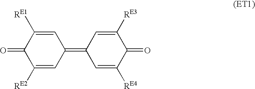
Advantageously, at least one of the electron transport substances is selected from the acceptor compounds represented by the following general formulas (ET1) to (ET15).
Figure US06485873-20021126-C00002
In the formula (ET1), each of RE1 to RE4 is independently a hydrogen atom, an alkyl group of 1 to 12 carbon atoms, an alkoxyl group of 1 to 12 carbon atoms, an optionally substituted aryl group, a cycloalkyl group, an optionally substituted aralkyl group, or an alkyl halide group. The substituent in the formula (ET1) is a halogen atom, an alkyl group of 1 to 6 carbon atoms, an alkoxyl group of 1 to 6 carbon atoms, a hydroxyl group, a cyano group, an amino group, a nitro group, or an alkyl halide group.
Figure US06485873-20021126-C00003
In the formula (ET2), each of RE5 to RE8 is independently a hydrogen atom, an alkyl group of 1 to 12 carbon atoms, an alkoxyl group of 1 to 12 carbon atoms, an optionally substituted aryl group, a cycloalkyl group, an optionally substituted aralkyl group, or an alkyl halide group. The substituent in the formula (ET2) is a halogen atom, an alkyl group of 1 to 6 carbon atoms, an alkoxyl group of 1 to 6 carbon atoms, a hydroxyl group, a cyano group, an amino group, a nitro group, or an alkyl halide group.
Figure US06485873-20021126-C00004
In the formula (ET3), each of RE9 to RE10 is independently a hydrogen atom, an alkyl group of 1 to 12 carbon atoms, an alkoxyl group of 1 to 12 carbon atoms, an optionally substituted aryl group, a cycloalkyl group, an optionally substituted aralkyl group, or an alkyl halide group. The substituent in the formula (ET3) is a halogen atom, an alkyl group of 1 to 6 carbon atoms, an alkoxyl group of 1 to 6 carbon atoms, a hydroxyl group, a cyano group, an amino group, a nitro group, or an alkyl halide group.
Figure US06485873-20021126-C00005
In the formula (ET4), each of RE11 and RE12 is independently a hydrogen atom, an alkyl group of 1 to 12 carbon atoms, an alkoxyl group of 1 to 12 carbon atoms, an optionally substituted aryl group, a cycloalkyl group, an optionally substituted aralkyl group, or an alkyl halide group. Each of RE13 to RE17 is independently a hydrogen atom, a halogen atom, an alkyl group of 1 to 12 carbon atoms, an alkoxyl group of 1 to 12 carbon atoms, an optionally substituted aryl group, an optionally substituted aralkyl group, an optionally substituted phenoxy group, or an alkyl halide group, wherein two or more of the groups may bond one another to for a ring. The substituent in the formula (ET4) is a halogen atom, an alkyl group of 1 to 6 carbon atoms, an alkoxyl group of 1 to 6 carbon atoms, a hydroxyl group, a cyano group, an amino group, a nitro group, or an alkyl halide group.
Figure US06485873-20021126-C00006
In the formula (ET5), each of RE18 to RE21 is independently a hydrogen atom, an alkyl group of 1 to 12 carbon atoms, an alkoxyl group of 1 to 12 carbon atoms, an optionally substituted aryl group, a cycloalkyl group, an optionally substituted aralkyl group, or an alkyl halide group. Each of RE22 and RE23 is independently a hydrogen atom, or an alkyl group of 1 to 12 carbon atoms. Each of RE24 to RE31 is independently a hydrogen atom, a halogen atom, an alkyl group of 1 to 12 carbon atoms, an alkoxyl group of 1 to 12 carbon atoms, an optionally substituted aryl group, or an alkyl halide group. The substituent in the formula (ET5) is a halogen atom, an alkyl group of 1 to 6 carbon atoms, an alkoxyl group of 1 to 6 carbon atoms, a hydroxyl group, a cyano group, an amino group, a nitro group, or an alkyl halide group.
Figure US06485873-20021126-C00007
In the formula (ET6), each of RE32 to RE36 is independently a hydrogen atom, a halogen atom, a cyano group, a nitro group, an alkyl group of 1 to 12 carbon atoms, an alkoxyl group of 1 to 12 carbon atoms, an optionally substituted aryl group, an optionally substituted aralkyl group, an optionally substituted phenoxy group, or an alkyl halide group. Each of RE37 to RE44 is a hydrogen atom or a nitro group, at least three of the RE37 to RS being nitro groups. The substituent in the formula (ET6) is a halogen atom, an alkyl group of 1 to 6 carbon atoms, an alkoxyl group of 1 to 6 carbon atoms, a hydroxyl group, a cyano group, an amino group, a nitro group, or an alkyl halide group.
Figure US06485873-20021126-C00008
In the formula (ET7), RE45 is an optionally substituted alkyl group or an optionally substituted aryl group. RE46 is an optionally substituted alkyl group, an optionally substituted aryl group, or a group represented by the following formula (ET7a), in which RE47 is an optionally substituted alkyl group or an optionally substituted aryl group.
—O—RE47  (ET7a)
The substituent in the formula (ET7) and the formula (ET7a) is a halogen atom, an alkyl group of 1 to 6 carbon atoms, an alkoxyl group of 1 to 6 carbon atoms, a hydroxyl group, a cyano group, an amino group, a nitro group, or an alkyl halide group.
Figure US06485873-20021126-C00009
In the formula (ET8), each of RE48 to RE60 is independently a hydrogen atom, an alkyl group of 1 to 6 carbon atoms, an alkoxyl group of 1 to 6 carbon atoms, an aryl group, an aralkyl group, a halogen atom, or an alkyl halide group.
Figure US06485873-20021126-C00010
In the formula (ET9), each of RE61 to RE68 is independently a hydrogen atom, an alkyl group of 1 to 6 carbon atoms, an alkoxyl group of 1 to 6 carbon atoms, an aryl group, an aralkyl group, a halogen atom, or an alkyl halide group.
Figure US06485873-20021126-C00011
In the formula (ET10), each of RE69 and RE70 is independently a cyano group or an alkoxycarbonyl group. RE71 is a hydrogen atom, an alkyl group of 1 to 12 carbon atoms, or an optionally substituted aryl group. Each of RE72 to RE76 is independently a hydrogen atom, a halogen atom, an alkyl group of 1 to 12 carbon atoms, an alkoxyl group, an optionally substituted aryl group, an alkyl halide group, or alkyl-substituted amino group. Each of RE77 to RE79 is independently a hydrogen atom or an alkyl group of 1 to 12 carbon atoms. Each of RE80 and RE81 is independently a hydrogen atom, halogen atom, an alkyl group of 1 to 12 carbon atoms, or an optionally substituted aryl group. X is a sulfur atom or an oxygen atom, n is 0 or 1. The substituent in the formula (ET10) is a halogen atom, an alkyl group of 1 to 6 carbon atoms, an alkoxyl group of 1 to 6 carbon atoms, a hydroxyl group, a cyano group, an amino group, a nitro group, or an alkyl halide group.
Figure US06485873-20021126-C00012
In the formulas (ET11). (ET12), and (ET13), each of RE82 to RE85 is independently a hydrogen atom or a halogen atom. Each of RE86 and RE87 is independently a cyano group or an alkoxycarbonyl group. Each of RE88 to RE92 is independently a hydrogen atom, a halogen atom, an alkyl group of 1 to 6 carbon atoms, a nitro group, or a cyano group.
Figure US06485873-20021126-C00013
In the formulas (ET14) and (ET15), each of RE93 to RE96 is independently a hydrogen atom or a halogen atom. Each of RE97 and RE98 is independently a cyano group or an alkoxycarbonyl group. Each of RE99 to RE103 is independently a hydrogen atom, a halogen atom, an alkyl group of 1 to 6 carbon atoms, a nitro group, or a cyano group.
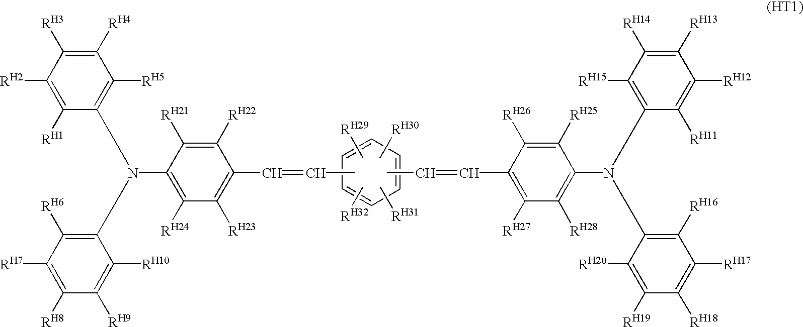
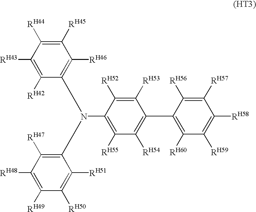
Advantageously, at least one of the hole transport substances is a compound represented by the following general formulas (HT1) to (HT5).
Figure US06485873-20021126-C00014
In the formula (HT1), each of RH1-RH32 is independently a hydrogen atom, an alkyl group of 1 to 6 carbon atoms, or an alkoxyl group of 1 to 6 carbon atoms.
Figure US06485873-20021126-C00015
In the formula (HT2), RH33 is a hydrogen atom or an alkyl group of 1 to 6 carbon atoms. Each of RH34 and RH35 is independently a hydrogen atom, an alkyl group of 1 to 6 carbon atoms, an alkoxyl group of 1 to 6 carbon atoms, or an optionally substituted aryl group, in which RH34 and RH35 may bond each other to form a ring, directly or through a carbon chain, an oxygen atom, or a sulfur atom. Each of RH36 and RH37 is independently an alkyl group of 1 to 12 carbon atoms, an optionally substituted cycloalkyl group of 3 to 12 carbon atoms, an optionally substituted aryl group, or an optionally substituted aralkyl group. Each of RH38 to RH41 is independently a hydrogen atom, an alkyl group of 1 to 6 carbon atoms, an alkoxyl group of 1 to 6 carbon atoms, or an optionally substituted aryl group. Two or more of the RH36 to RH41 may bond one another to form a ring, directly or through a carbon chain, an oxygen atom, or a sulfur atom. m is 0 or 1. The substituent in the formula (HT2) is a halogen atom, an alkyl group of 1 to 6 carbon atoms, an alkoxyl group of 1 to 6 carbon atoms, an optionally substituted aryl group, a hydroxyl group, a cyano group, an amino group, a nitro group, an alkyl halide group, or an alkyl-substituted amino group. Two or more of these substituent groups may bond one another to form a ring, directly or through a carbon chain, an oxygen atom, or a sulfur atom.
Figure US06485873-20021126-C00016
In the formula (HT3), each of RH42 to RH60 is independently a hydrogen atom, a halogen atom, an alkyl group of 1 to 12 carbon atoms, an alkoxyl group of 1 to 12 carbon atoms, an alkyl-substituted amino group, or an optionally substituted aryl group, in which two or more of RH42 to RH60 may bond one another to form a ring, directly or through a carbon chain, an oxygen atom, or a sulfur atom. The substituent in the formula (HT3) is a halogen atom, an alkyl group of 1 to 6 carbon atoms, an alkoxyl group of 1 to 6 carbon atoms, a hydroxyl group, a cyano group, an amino group, a nitro group, or an alkyl halide group, in which two or more of these substituent groups may bond one another to form a ring, directly or through a carbon chain, an oxygen atom, or a sulfur atom.
Figure US06485873-20021126-C00017
In the formula (HT4), each of RH61 to RH88 is independently a hydrogen atom, a halogen atom, an aryl group, an alkyl group of 1 to 12 carbon atoms, an alkoxyl group of 1 to 12 carbon atoms or an optionally substituted aryl group. The substituent in the formula (HT4) is a halogen atom, an alkyl group of 1 to 6 carbon atoms, or an alkoxyl group of 1 to 6 carbon atoms.
Figure US06485873-20021126-C00018
In the formula (HT5), each of RH89 to RH92 is independently an alkyl group of 1 to 6 carbon atoms, or an optionally substituted aralkyl group. Each of RH93 to RH102 is independently a hydrogen atom, a halogen atom, an alkyl group of 1 to 6 carbon atoms, or an alkoxyl group of 1 to 6 carbon atoms. The substituent in the formula (HT5) is a halogen atom, an alkyl group of 1 to 6 carbon atoms, or an alkoxyl group of 1 to 6 carbon atoms.
Advantageously, at least one of the charge generation substances is an X-type metal-free phthalocyanine.
Advantageously, at least one of the resin binder is polycarbonate having a structural unit represented by the general formula (BD1) below as a principal repeating unit.
Figure US06485873-20021126-C00019
In the formula (BD1), each of RB1 to RB8 is independently a hydrogen atom, an alkyl group of 1 to 6 carbon atoms, an optionally substituted aryl group, a cycloalkyl group, or an halogen atom. Z is a group of atoms needed to form an optionally substituted carbon ring. The substituent in the formula (BD1) is an alkyl group of 1 to 6 carbon atoms or a halogen atom.
The electrophotographic apparatus of the present invention is provided with the above-described electrophotographic photoconductor of the present invention. The charging process of the electrophotographic apparatus of the present invention is performed by a positive-charging process.
Although a definite mechanism of how the present invention leads to excellent electrical characteristics in positive-charging process and improved stability is not thoroughly understood, it may be assumed that the favorable results are brought about by the effect of the biphenyl derivative to suppress undesirable trapping of electrons during electron transport by the electron transport substance, and are not caused by the effects as a plasticizer agent, as a deactivating agent, as an agent for increasing electrostatic force or van der Vaals' force, or resistance to NOx.
The invention will be described with reference to some preferred embodiments thereof and the accompanying drawing.
Structure of Layers
FIG. 1 is a cross sectional view showing an electrophotographic photoconductor according to the present invention. An undercoat layer 2 is coated on a conductive substrate 1. A photosensitive layer 3 and an optional protection layer 4 are then subsequently coated on conductive substrate 1. Undercoat layer 2 and protection layer 4 are provided as needed. Photosensitive layer 3 of the present invention is preferably of a single-layer type, performing both a charge generation function and a charge transport function.
Conductive Substrate
Conductive substrate 1, acting as a support for the other layers, functions as an electrode of the photoconductor. Conductive substrate 1 may have a cylindrical shape, planar shape, or film-like shape, and may be formed of a metal, such as aluminum, stainless steel or nickel, or glass or resin that has been treated to be given a certain conductivity.
Undercoat layer
Undercoat layer 2, which may be formed of a layer containing a resin as a major component, or of an oxide film such as alumite, is provided as needed for the purposes of preventing unnecessary charges from injecting from conductive substrate 1 into photosensitive layer 3. Undercoat layer 2 also acts to cover defects on the surface of conductive substrate 1, and improving the adhesivity of photosensitive layer 3.
The binder resin of undercoat layer 2 is preferably selected from polycarbonate resin, polyester resin, polyvinylacetal resin, polyvinylbutyral resin, polyvinylalcohol resin, vinylchloride resin, vinylacetate resin, polyethylene, polypropylene, acrylic resin, polyurethane resin, epoxy resin, melamine resin, silicon resin, polyamide resin, polystyrene resin, polyacetal resin, polyarylate resin, polysulfone resin, and polymer of methacrylic acid ester, and copolymers of these resins, which may be used in suitable combination. A mixture of resins of the same species but different molecular weight may also be used as a binder resin.
The binder resin may contain fine particles of a metal oxide, such as silicon oxide (silica), titanium oxide, zinc oxide, calcium oxide, aluminum oxide (alumina), or zirconium oxide, a metal sulfate, such as barium sulfate or calcium sulfate, or a metal nitride, such as silicon nitride or aluminum nitride. Alternatively, the binder resin may contain an organic metal compound, a silane coupling agent, or a material formed of an organic metal compound and a silane coupling agent. The content of these additives may be set to a desired value within a range in which an undercoat layer can be actually formed.
Undercoat layer 2, which is formed of a resin as a major component, may contain a charge transport substance for the purpose to give charge transport ability or to suppress charge trapping. The content of such charge transport substance is from about 0.1 to about 60 wt. %, preferably from about 5 to about 40 wt. % with respect to a solid component of undercoat layer 2. Undercoat layer 2 may further contain other known additives as needed, so far as the additives don't much deteriorate electrophotographic characteristics.
Although undercoat layer 2 may be used in the form of a single-layer, undercoat layer 2 may also be used in a form of a laminate, consisting of two or more different layers. While the film thickness of undercoat layer 2 depends on the composition of the materials used in the layer, the film thickness may be set to a desired value within a range in which the photoconductor does not suffer from adverse influences, such as an increase in the residual potential, when it is repeatedly and continuously used. The film thickness of undercoat layer 2 is preferably from about 0.1 μm to about 10 μm.
Photosensitive Layer
Photosensitive layer 3 is principally formed of a resin binder, a charge generation substance, a hole transport substance, and an electron transport substance. Photosensitive layer 3, according to the present invention, is a single-layer containing a biphenyl derivative.
The biphenyl derivatives used in the present invention preferably have the structural formula represented by the general formula(BP1). More preferably, the biphenyl derivative is a compound selected from the group consisting of the biphenyl represented by the formula (BP1-1), o-terphenyl represented by the formula (BP1-4), m-terphenyl represented by the formula (BP1-3), p-terphenyl represented by the formula (BP1-2), p-benzylbiphenyl represented by formula (BP1-5), and hydrogenated terphenyl represented by the formulas (BP1-6)-(BP1-8). A mixture of two or more of the compounds of the formula (BP1) may also be used in the invention. Specific examples of such biphenyl derivatives include the compounds represented by the structural formulas (BP1-1)-(BP1-78), but are not limited to those compounds. The content of the biphenyl derivative is in the range from about 0.1 to about 20 wt. %, preferably from about 0.5 to about 10 wt. % with respect to a solid component of photosensitive layer 3.
Figure US06485873-20021126-C00020
Figure US06485873-20021126-C00021
Figure US06485873-20021126-C00022
Figure US06485873-20021126-C00023
Figure US06485873-20021126-C00024
Figure US06485873-20021126-C00025
Figure US06485873-20021126-C00026
The charge generation substance in the present invention is preferably a phthalocyanine pigment, a naphthalocyanine pigment, an azo pigment, a polycyclic quinone pigment such as anthraquinone and anthanthrone, a perylene pigment, a perynone pigment, a squarylium dye, an azulenium dye, a thiapyrylium dye, a cyanine dye, a quinacridone dye, and any combination of these pigments and dyes may be used. More preferably, the charge generation substance are pigments including disazo pigments and trisazo pigments as azo pigments, 3,9-dibromo anthanthrone as an anthanthrone pigment, N-N′-bis(3,5dimethylphenyl)-3,4:9,10-perylene bis(carboxyimide) as a perylene pigment, metal-free phthalocyanine, copper phthalocyanine, and titanylphthalocyanine as phthalocyanines, in particular, X-type metal-free phthalocyanine, τ-type metal-free phthalocyanine, ε-type copper phthalocyanine, α-type titanylphthalocyanine, β-type titanylphthalocyanine, amorphous titanylphthalocyanine, Y-type titanylphthalocyanine, I-type titanylphthalocyanine, and the titanylphthalocyanine disclosed in Japanese unexamined patent application publication No. H8-209023, exhibiting a maximum peak at 9.6° of Bragg angle 2θ in an X-ray diffraction spectrum observed with Cu Kα radiation. The content of such charge generation substance is in the range from about 0.1 to about 20 wt. %, preferably from about 0.5 to about 10 wt. %.
The electron transport substance is preferaby selected from the compounds represented by the above-described general formulas (ET1) to (ET15). Other electron transport substances which may be suitably used include succinic anhydride, maleic anhydride, dibromosuccinic anhydride, phthalic anhydride, 3-nitrophthalic anhydride, 4-nitrophthalic anhydride, pyromellitic anhydride, pyromellitic acid, trimellitic acid, trimellitic anhydride, phthalimide, 4-nitro phthalimide, tetracyanoethylene, tetracyanoquinodimethane, chloranil, bromanil, o-nitro benzoic acid, malononitrile, trinitrofluorenone, trinitrothioxanthone, dinitrobenzene, dinitroanthracene, dinitroacridine, nitroanthraquinone, dinitroanthraquinon, thiopyran compounds, quinone compounds, benzoquinone compounds, diphenoquinone compounds, naphthoquinone compounds, anthraquinone compounds, stilbenequinone compounds, and any appropriate combination of these compounds. The specific examples of the compounds represented by the general formulas (ET1) to (ET15) include the compounds represented by the following structural formulas (ET1-1)-(ET15-16). The specific examples of the other electron transport substances include the compounds represented by the structural formulas (ET-1)-(ET-42), but are not limited to those compounds.
The content of the electron transport substance is in the range from about 1 to about 50 wt. %, preferably from about 5 to about 40 wt. % with respect to the solid component of the photosensitive layer.
Figure US06485873-20021126-C00027
Figure US06485873-20021126-C00028
Figure US06485873-20021126-C00029
Figure US06485873-20021126-C00030
Figure US06485873-20021126-C00031
Figure US06485873-20021126-C00032
Figure US06485873-20021126-C00033
Figure US06485873-20021126-C00034
Figure US06485873-20021126-C00035
Figure US06485873-20021126-C00036
Figure US06485873-20021126-C00037
Figure US06485873-20021126-C00038
Figure US06485873-20021126-C00039
Figure US06485873-20021126-C00040
Figure US06485873-20021126-C00041
Figure US06485873-20021126-C00042
Figure US06485873-20021126-C00043
Figure US06485873-20021126-C00044
Figure US06485873-20021126-C00045
Figure US06485873-20021126-C00046
Figure US06485873-20021126-C00047
Figure US06485873-20021126-C00048
Figure US06485873-20021126-C00049
Figure US06485873-20021126-C00050
Figure US06485873-20021126-C00051
Figure US06485873-20021126-C00052
Figure US06485873-20021126-C00053
Figure US06485873-20021126-C00054
Figure US06485873-20021126-C00055
Figure US06485873-20021126-C00056
The hole transport substance is preferably selected from the compounds represented by the general formulas (HT1) to (HT5). Other hole transport substances which may be used include a hydrazone compound, a pyrazoline compound, a pyrazolone compound, an oxadiazole compound, an oxazole compound, an arylamine compound, a benzidine compound, a stilbene compound, a styryl compound, polyvinylcarbazole, polysilane, and an appropriate combination of these hole transport substances. The specific compounds represented by the general formulas (HT1) to (HT5) include the compounds represented by the following structural formulas (HT1-1) to (HT5-10). The specific examples of the other hole transport substance include the compounds represented by the following structural formulas (HT-1) to (HT-37), but are not limited to those compounds.
The content of the hole transport substance is in the range from about 5 to about 80 wt. %, preferably from about 10 to about 60 wt. % with respect to the solid component of the photosensitive layer.
Figure US06485873-20021126-C00057
Figure US06485873-20021126-C00058
Figure US06485873-20021126-C00059
Figure US06485873-20021126-C00060
Figure US06485873-20021126-C00061
Figure US06485873-20021126-C00062
Figure US06485873-20021126-C00063
Figure US06485873-20021126-C00064
Figure US06485873-20021126-C00065
Figure US06485873-20021126-C00066
Figure US06485873-20021126-C00067
Figure US06485873-20021126-C00068
Figure US06485873-20021126-C00069
Figure US06485873-20021126-C00070
Figure US06485873-20021126-C00071
Figure US06485873-20021126-C00072
Figure US06485873-20021126-C00073
Figure US06485873-20021126-C00074
Figure US06485873-20021126-C00075
Figure US06485873-20021126-C00076
Figure US06485873-20021126-C00077
Figure US06485873-20021126-C00078
Figure US06485873-20021126-C00079
Figure US06485873-20021126-C00080
Figure US06485873-20021126-C00081
Figure US06485873-20021126-C00082
Figure US06485873-20021126-C00083
Figure US06485873-20021126-C00084
Figure US06485873-20021126-C00085
Figure US06485873-20021126-C00086
Figure US06485873-20021126-C00087
Figure US06485873-20021126-C00088
Figure US06485873-20021126-C00089
Figure US06485873-20021126-C00090
Figure US06485873-20021126-C00091
Figure US06485873-20021126-C00092
Figure US06485873-20021126-C00093
Figure US06485873-20021126-C00094
Figure US06485873-20021126-C00095
Figure US06485873-20021126-C00096
Figure US06485873-20021126-C00097
Figure US06485873-20021126-C00098
Figure US06485873-20021126-C00099
Figure US06485873-20021126-C00100
Figure US06485873-20021126-C00101
Figure US06485873-20021126-C00102
Figure US06485873-20021126-C00103
The resin binder of photosensitive layer 3 may be selected from polycarbonate resin, polyester resin, polyvinylacetal resin, polyvinylbutyral resin, polyvinylalcohol resin, vinylchloride resin, vinylacetate resin, polyethylene, polypropylene, acrylic resin, polyurethane resin, epoxy resin, melamine resin, silicone resin, polyamide resin, polystylene resin, polyacetal resin, polyarylate resin, polysulfone resin, and polymer of methacrylic acid ester, and copolymers of these resins, which may be used in suitable combination. In particular, polycarbonates, in which bisphenol Z type polycarbonate is a typical one, having the principal repeating unit represented by the general formula (BD1) may be suitably used. The specific examples of the polycarbonates include the polycarbonates having the repeating unit represented by the following structural formulas (BD1-1) to (BD1-16). Alternatively, any polycarbonate resin, having one or more repeating units represented by the following structural units (BD-1)-(BD7), as well as any polyester resin, may be used, but are not limited to those resins. A mixture of resins of the same species, but different molecular weight, may also be used as a binder resin.
The content of the binder resin is in the range from about 10 to about 90 wt. %, preferably from about 20 to about 80 wt. % with respect to the solid component of the photosensitive layer.
Figure US06485873-20021126-C00104
Figure US06485873-20021126-C00105
Figure US06485873-20021126-C00106
The film thickness of the photosensitive layer is preferably in a range from about 3 to about 100 μm, more preferably from about 10 to about 50 μm, so as to maintain a practically effective surface potential.
Photosensitive layer 3 may contain an antioxidant or a photo-stabilizing agent to enable photosensitive layer 3 to withstand hazardous environment or improve stability against hazardous light. The compound used for these purposes may be selected from chromanol derivatives such as tocopherol, polyarylalkane compounds, hydroquinone derivatives, benzophenone derivatives, benzotriazole derivatives, thioether compounds, phenylene diamine derivatives, phosphonic ester, phosphorous ester, phenol compounds, hindered phenol compounds, straight chain amine compounds, cyclic amine compounds, and hindered amine compounds.
Photosensitive layer 3 may contain a leveling agent such as silicone oil or fluoro oil for improving flatness and lubrication performance of the formed film.
Photosensitive layer 3 may further contain, for the purposes of reducing friction coefficient and providing lubrication, fine particles of a metal oxide, such as silicon oxide (silica), titanium oxide, zinc oxide, calcium oxide, aluminum oxide (alumina), or zirconium oxide, a metal sulfate such as barium sulfate or calcium sulfate, a metal nitride such as silicon nitride or aluminum nitride, particles of fluororesin, such as tetrafluoroethylene resin, or comb-type graft polymerized fluororesin.
Further, photosensitive layer 3 may contain other known additives as needed, in the range in which electrophotographic characteristics are not much deteriorated.
Protection Layer
Protection layer 4 may be provided, as needed, to improve durability in repeated printings. Protection layer 4 is preferably formed from a layer of a resin binder as a major component, or a thin film of inorganic material, such as amorphous carbon. The binder resin of protection layer 4 may contain, to improve electrical conductivity, reduce friction coefficient, or provide lubrication, fine particles of a metal oxide, such as silicon oxide (silica), titanium oxide, zinc oxide, calcium oxide, aluminum oxide (alumina), or zirconium oxide, a metal sulfate such as barium sulfate or calcium sulfate, a metal nitride such as silicon nitride or aluminum nitride, particles of fluororesin such as tetrafluoroethylene resin, or comb-type graft polymerized fluororesin.
Protection layer 4 may further contain a hole transport substance or an electron transport substance used in photosensitive layer 3, to provide charge transport capability. Protection layer 4 may also contain a leveling agent, such as silicone oil or fluoro oil, to improve flatness or provide lubrication of the formed film. Other known additives may be contained, as needed, in a range in which electrophotographic characteristics are not significantly deteriorated.
Method for Forming Layers
A preferred processes is described for forming undercoat layer 2, photosensitive layer 3, and protection layer 4. A coating liquid for each of the layers is prepared by dissolving and dispersing the materials described above in an appropriate solvent. The coating liquid is then coated by an appropriate coating method and dried.
The solvent is preferably selected from alcohols such as methanol, ethanol, n-propanol, i-propanol, n-butanol, and benzylalcohol, ketons such as acetone, MEK (methyl ethyl keton), methylisobutyl keton, and cyclohexanone, amides such as DMF (dimethy folmaldehyde) and dimethy acetoamide, sulfoxide such as dimethysulfoxide, cyclic and straight chain ethers such as THF (tetrahydrofuran), dioxane, dioxolane, diethylether, methyl cellosolve, and ethyl cellosolve, esters such as methyl acetate, ethyl acetate, and n-butyl acetate, aliphatic hydrocarbon halides such as methylene chloride, chloroform, carbon tetrachloride, dichloroethylene, trichloroethylene, mineral oils such as ligroin, aromatic hydrocarbons such as benzene, toluene, and xylene, aromatic hydrocarbon halides such as chlorobenzene and dichlorobenzene, and any mixture thereof.
The method for dissolving and dispersing the coating liquid is preferably selected from known methods including beads mill such as paint shaker, ball mill and DYNO-MIL® (manufactured by Wab Co.), and ultrasonic dispersion. The coating method is preferably selected from known methods including dip-coating, seal-coating, spray-coating, bar-coating and blade-coating.
Temperature and time of the drying process is decided in view of the solvent used and a manufacturing cost. Preferably, drying temperature is in the range from room temperature to 200° C., and the drying time is from 10 minutes to 2 hours. More preferably, drying temperature is from a boiling point of the solvent to a temperature 80° C. higher than the boiling point. The drying process is usually conducted under the atmospheric pressure or lower pressure, and in a static or ventilated place.
EXAMPLES
The present invention will be described in greater detail referring to some preferred embodiment examples.
Photoconductor Example 1 (E1)
A plate shape photoconductor was fabricated for evaluating electrical characteristics. A drum shape photoconductor (30 mm diameter) was fabricated for evaluating printing performances. Each of an aluminum plate and an aluminum blank tube was dipped in a coating solution for forming an undercoat layer, and dried at 100° C. for 60 minutes to obtain an undercoat layer having a film thickness of 0.3 μm. The coating solution for the undercoat layer had a composition as follows:
3 parts soluble nylon (AMILAN CM8000 available from Toray Industries, Inc.), and
97 parts mixed solvent of methanol and methylene chloride with weight ratio 5/5.
Dispersion liquid for a photosensitive layer was prepared by dispersing a mixture of the materials listed below in a DYNO-MIL® (manufactured by Wab Co.). Each of the aluminum plate and the aluminum tube coated with the undercoat layer was dipped in the dispersion liquid for forming a single-layer photosensitive layer, and dried at 100° C. for 60 minutes to obtain a single-layer photosensitive layer having a film thickness of 25 μm. The mixture for preparing the dispersion liquid had a composition as follows:
0.2 parts charge transport substance: X-type metal-free phthalocyanine,
0.5 parts biphenyl derivative: the compound of formula (BP1-1),
3 parts electron transport substance: the compound of formula (ET1-8),
5 parts hole transport substance: the compound of formula (HT1-66),
0.5 parts antioxidant agent: BHT (2,6-di-t-butyl-4-methylphenol),
0.01 part silicone oil: KF-50 available from Shin'etsu Chemical Industries Co., Ltd.
11 parts binder resin: bisphenol Z polycarbonate resin,
a resin having the structural unit of formula (BD1-1): PANLITE
TS2020 available from Teijin Chemicals Ltd., and
100 parts methylene chloride.
Thus, the electrophotographic photoconductor of Example 1 was fabricated.
Photoconductor Examples 2 to 44 (E2 to E44) and Comparative Examples 1 to 21 (C1 to C21)
Photoconductor Examples 2 to 44 and Comparative Examples 1 to 21 were fabricated in the same manner as in Example 1 except that biphenyl derivative, electron transport substance, and hole transport substance were replaced by those indicated in Tables 1, 2 and 3.
TABLE 1
electron hole
biphenyl transport transport
specimen derivative substance substance
E1 (BP1-1) (ET1-8) (HT1-66)
E2 (BP1-2) (ET1-8) (HT1-66)
E3 (BP1-3) (ET1-8) (HT1-66)
E4 (BP1-4) (ET1-8) (HT1-66)
E5 (BP1-5) (ET1-8) (HT1-66)
E6 (BP1-6) (ET1-8) (HT1-66)
E7 (BP1-1) (ET2-11) (HT2-22)
E8 (BP1-2) (ET2-11) (HT2-22)
E9 (BP1-3) (ET2-11) (HT2-22)
E10 (BP1-4) (ET2-11) (HT2-22)
E11 (BP1-5) (ET2-11) (HT2-22)
E12 (BP1-6) (ET2-11) (HT2-22)
E13 (BP1-1) (ET3-2) (HT3-30)
E14 (BP1-2) (ET3-2) (HT3-30)
E15 (BP1-3) (ET3-2) (HT3-30)
E16 (BP1-4) (ET3-2) (HT3-30)
E17 (BP1-5) (ET3-2) (HT3-30)
E18 (BP1-6) (ET3-2) (HT3-30)
E19 (BP1-1) (ET4-5) (HT1-101)
E20 (BP1-2) (ET4-5) (HT1-101)
E21 (BP1-3) (ET4-5) (HT1-101)
E22 (BP1-4) (ET4-5) (HT1-101)
E23 (BP1-5) (ET4-5) (HT1-101)
E24 (BP1-6) (ET4-5) (HT1-101)
TABLE 2
electron hole
biphenyl transport transport
specimen derivative substance substance
E25 (BP1-1) (ET4-5) (HT2-34)
E26 (BP1-2) (ET4-5) (HT2-34)
E27 (BP1-3) (ET4-5) (HT2-34)
E28 (BP1-4) (ET4-5) (HT2-34)
E29 (BP1-5) (ET4-5) (HT2-34)
E30 (BP1-6) (ET4-5) (HT2-34)
E31 (BP1-3) (ET4-5) (HT3-3)
E32 (BP1-3) (ET4-5) (HT4-2)
E33 (BP1-3) (ET4-5) (HT5-4)
E34 (BP1-3) (ET4-5) (HT-11)
E35 (BP1-3) (ET4-5) (HT-25)
E36 (BP1-3) (ET5-1) (HT3-19)
E37 (BP1-3) (ET6-6) (HT2-12)
E38 (BP1-3) (ET7-12) (ET4-2)
E39 (BP1-3) (ET8-2) (HT1-4)
E40 (BP1-3) (ET9-1) (HT1-4)
E41 (BP1-3) (ET10-2) (HT3-3)
E42 (BP1-3) (ET12-3) (HT2-9)
E43 (BP1-3) (ET14-2) (HT2-9)
E44 (BP1-3) (ET-10) (HT1-101)
TABLE 3
electron hole
biphenyl transport transport
specimen derivative substance substance
C1 none (ET1-8) (HT1-66)
C2 none (ET2-11) (HT2-22)
C3 none (ET3-2) (HT3-30)
C4 none (ET4-5) (HT1-101)
C5 none (ET4-5) (HT2-34)
C6 none (ET5-1) (HT3-19)
C7 none (ET6-6) (HT2-12)
C8 none (ET7-12) (HT4-2)
C9 none (ET8-2) (HT1-4)
C10 none (ET9-1) (HT1-4)
C11 none (ET10-2) (HT3-3)
C12 none (ET12-3) (HT2-9)
C13 none (ET14-2) (HT2-9)
C14 none (ET-10) (HT1-101)
C15 BP1-1 none (HT1-101)
C16 BP1-2 none (HT1-101)
C17 BP1-3 none (HT1-101)
C18 BP1-4 none (HT1-101)
C19 BP1-5 none (HT1-101)
C20 BP1-6 none (HT1-101)
C21 none none (HT1-101)
TABLE 4
electrical characteristics image quality (under high temp & humidity)
by EPA-800 by HL-730
retention sensitivity residual initial image after 5,000 printings
rate Vk5 E1/2 potential entirely entirely entirely entirely
specimen (%) μJ/cm2 Vr(V) black image white image black image white image
E1  84.4 0.54 73 good(1.44) good(0.05) good(1.38) good(0.04)
E2  83.2 0.57 70 good(1.44) good(0.04) good(1.32) good(0.04)
E3  80.3 0.55 72 good(1.43) good(0.05) good(1.37) good(0.08)
E4  85.2 0.54 77 good(1.44) good(0.05) good(1.34) good(0.05)
E5  83.0 0.60 80 good(1.42) good(0.05) good(1.34) good(0.07)
E6  82.8 0.57 77 good(1.42) good(0.05) good(1.36) good(0.05)
E7  83.5 0.60 80 good(1.41) good(0.05) good(1.38) good(0.06)
E8  84.2 0.57 76 good(1.43) good(0.05) good(1.35) good(0.05)
E9  85.0 0.61 75 good(1,45) good(0.04) good(1.39) good(0.05)
E10 88.1 0.55 83 good(1.44) good(0.05) good(1.40) good(0.05)
E11 79.9 0.58 80 good(1.41) good(0.05) good(1.37) good(0.08)
E12 83.6 0.62 77 good(1.41) good(0.06) good(1.34) good(0.07)
E13 87.5 0.69 75 good(1.42) good(0.06) good(1.39) good(0.10)
E14 84.2 0.65 69 good(1.45) good(0.05) good(1.32) good(0.09)
E15 81.0 0.66 70 good(1.42) good(0.05) good(1.38) good(0.06)
E16 79.9 0.68 70 good(1.43) good(0.05) good(1.36) good(0.04)
E17 82.2 0.71 73 good(1.44) good(0.04) good(1.35) good(0.05)
E18 81.9 0.65 68 good(1.44) good(0.05) good(1.35) good(0.05)
E19 85.7 0.44 65 good(1.42) good(0.05) good(1.38) good(0.05)
E20 86.4 0.42 60 good(1.46) good(0.05) good(1.32) good(0.06)
E21 86.2 0.41 59 good(1.43) good(0.05) good(1.33) good(0.07)
E22 87.1 0.42 63 good(1.44) good(0.05) good(1.37) good(0.08)
TABLE 5
electrical characteristics image quality (under high temp & humidity)
by EPA-800 by HL-730
retention sensitivity residual initial image after 5,000 printings
rate Vk5 E1/2 potential entirely entirely entirely entirely
specimen (%) μJ/cm2 Vr(V) black image white image black image white image
E23 88.0 0.42 66 good(1.43) good(0.04) good(1.38) good(0.06)
E24 86.5 0.48 70 good(1.42) good(0.05) good(1.40) good(0.06)
E25 85.0 0.49 57 good(1.42) good(0.05) good(1.33) good(0.07)
E26 82.9 0.52 60 good(1.44) good(0.05) good(1.37) good(0.05)
E27 82.7 0.47 58 good(1.45) good(0.05) good(1.36) good(0.06)
E28 84.0 0.54 60 good(1.43) good(0.04) good(1.33) good(0.05)
E29 86.0 0.48 59 good(1.45) good(0.04) good(1.40) good(0.05)
E30 81.3 0.48 65 good(1.41) good(0.05) good(1.37) good(0.08)
E31 83.6 0.55 70 good(1.43) good(0.05) good(1.37) good(0.09)
E32 84.0 0.53 78 good(1.42) good(0.05) good(1.41) good(0.06)
E33 86.0 0.49 80 good(1.42) good(0.04) good(1.37) good(0.06)
E34 81.4 0.74 90 good(1.40) good(0.05) good(1.36) good(0.05)
E35 78.6 0.68 86 good(1.44) good(0.05) good(1.34) good(0.05)
E36 86.7 0.88 88 good(1.45) good(0.05) good(1.31) good(0.06)
E37 85.6 0.92 96 good(1.40) good(0.04) good(1.39) good(0.04)
E38 82.5 0.70 75 good(1.44) good(0.05) good(1.38) good(0.07)
E39 84.5 0.95 89 good(1.38) good(0.05) good(1.37) good(0.06)
E40 82.6 0.91 94 good(1.41) good(0.05) good(1.40) good(0.05)
E41 88.6 0.87 87 good(1.41) good(0.05) good(1.40) good(0.05)
E42 84.4 0.84 90 good(1.37) good(0.04) good(1.29) good(0.08)
E43 81.9 0.90 93 good(1.39) good(0.05) good(1.33) good(0.08)
E44 79.6 1.05 112  good(1.35) good(0.05) good(1.34) good(0.08)
TABLE 6
electrical characteristics image quality (under high temp & humidity)
by EPA-800 by HL-730
retention sensitivity residual initial image after 5,000 printings
rate Vk5 E1/2 potential entirely entirely entirely entirely
specimen (%) μJ/cm2 Vr(V) black image white image black image white image
C1 84.8 0.54 68 good(1.42) good(0.04) good(1.35) poor(0.15)B
C2 83.7 0.55 71 good(1.42) good(0.05) poor(1.26)A poor(0.14)B
C3 87.6 0.68 66 good(1.43) good(0.05) poor(1.21)A poor(0.13)B
C4 86.0 0.43 59 good(1.40) good(0.04) good(1.34) poor(0.16)B
C5 82.2 0.47 56 good(1.44) good(0.05) poor(1.27)A poor(0.15)B
C6 85.5 0.91 87 good(1.39) good(0.04) good(1.32) poor(0.15)B
C7 85.9 0.89 94 good(1.43) good(0.05) good(1.33) poor(0.14)B
C8 84.5 0.70 75 good(1.43) good(0.05) poor(1.20)A poor(0.15)B
C9 83.0 0.94 91 good(1.44) good(0.05) poor(1.14)A poor(0.19)B
 C10 81.8 0.96 90 good(1.41) good(0.06) poor(1.22)A poor(0.16)B
 C11 86.1 0.90 86 good(1.40) good(0.05) good(1.30) poor(0.14)B
 C12 83.5 0.82 90 good(1.38) good(0.05) poor(1.27)A poor(0.24)B
 C13 80.5 0.88 89 good(1.39) good(0.04) good(1.32) poor(0.28)B
 C14 80.4 1.10 100  good(1.39) good(0.04) poor(1.3)A  poor(0.26)B
 C15 89.0 1.24 115  poor(1.21)A good(0.05) poor(1.19)A good(0.11)
TABLE 7
electrical characteristics image quality (under high temp & humidity)
by EPA-800 by HL-730
retention sensitivity residual initial image after 5,000 printings
rate Vk5 E1/2 potential entirely entirely entirely entirely
specimen (%) μJ/cm2 Vr(V) black image white image black image white image
C16 90.1 1.23 160 poor(1.15)A good(0.05) poor(1.22)A poor(0.16)B
C17 91.4 1.18 157 poor(1.27)A good(0.04) poor(1.07)A poor(0.20)B
C18 89.3 1.20 160 poor(1.09)A good(0.05) poor(1.13)A good(0.07)
C19 90.0 1.21 160 poor(1.11)A good(0.05) poor(1.19)A poor(0.28)B
C20 89.8 1.17 158 poor(1.25)A good(0.05) poor(1.21)A poor(0.19)B
C21 88.8 1.21 154 poor(1.22)A good(0.05) poor(1.09)A poor(0.24)B
Evaluation of Photoconductor Examples 1 to 44 and Comparative Examples 1 to 21
Evaluation of electrical characteristics was conducted on plate-shaped photoconductors using an electrostatic copying-paper testing apparatus: type EPA-8100 manufactured by Kawaguchi Electric Works Co., Ltd., as described below.
The surface of the photoconductor specimen was charged in the dark up to about +600 V under an environment having a temperature of 23° C. and a relative humidity of 50%. Then, the retention rate of surface potential in 5 seconds until light exposure was obtained. The retention rate is defined by the expression indicated below.
retention rate Vk5 (%)=V5/V0×100
Here, V0 is the surface voltage just after the end of charging, and V5 is the surface potential at 5 seconds after the end of charging (or just before start of light exposure).
Similarly, the surface of the photoconductor specimen was charged up to about +600 V. Then, the surface of the photoconductor was irradiated with monochromatic light generated by a halogen lamp and filtered to have a wavelength of 780 nm and intensity of 1.0 μW/cm2 for 5 seconds, so as to obtain the sensitivity E½(μJ/cm2) defined as an amount of exposed light required to attenuate the surface potential from +600 V to +300 V. Also, the residual potential Vr (V), defined as the surface potential at the end of the irradiation for 5 seconds was obtained.
Durability in actual printings was evaluated on a drum-shaped photoconductor mounted on a laser printer HL-730 manufactured by Brother Co., Ltd. An entirely black image and an entirely white image were printed under an environment having a temperature of 30° C. and a relative humidity of 75% (high temperature and high humidity environment). Evaluation of initial image was conducted by measuring density of the images using a densitometer: Macbeth RD914. Then, an image of printed area percentage of 5% was printed on 5,000 sheets of paper. After the 5,000 sheets of printings, the entirely black image and the entirely white image were printed to evaluate the image quality after 5,000 printings.
The results of these evaluations are shown in Tables 4 to 7.
In Tables 4 to 7, the numerals in the parenthesis in the columns for image quality, e.g., ‘poor (1.21) A’, are image density values measured by Macbeth densitometer. The standard image density value was set at 0.04 for a white image and at 1.77 for a black image.
Mark A for poor images, e.g., ‘poor (1.21) A’, means that printing of an entirely black image generated a partially faint and uneven image.
Mark B for poor images, e.g., ‘poor (0.15) B’, means that printing of an entirely white image generated numerous dots called fogging in a whole sheet.
Tables 4 to 7 shows that the photoconductors of Comparative Examples 15 to 21, containing no electron transport substance, caused high residual potential and resulted in the printed images of low density for an entirely black image under a high temperature and humidity environment. Also, Tables 4 to 7 indicate that the photoconductors of Comparative Examples 1 to 14, containing no biphenyl compound, resulted in the printed images displaying fogging for an entirely white image in the 5,000 sheets of test printings under a high temperature and humidity environment. In contrast, the photoconductors of the present invention, containing electron transport substance and a biphenyl compound, exhibited low residual potential, and generated no image defect in the initial printing and even after 5,000 printings under a high temperature and humidity environment. Thus, the photoconductors according to the present invention exhibited excellent residual potential and image characteristics.
According to the present invention, an electrophotographic photoconductor comprises a conductive substrate, and a single-layer photosensitive layer including at least a resin binder, a charge generation substance, a hole transport substance, and an electron transport substance. The photosensitive layer contains a biphenyl derivative. Such a photoconductor of the present invention exhibits low residual potential and excellent stability in various environments. Thus, the present invention provides an electrophotographic photoconductor having excellent characteristics. The photoconductors of the present invention are useful in printers, copiers, and facsimile machines employing electrophotographic technology.
Having described preferred embodiments of the invention with reference to the accompanying drawings, it is to be understood that the invention is not limited to those precise embodiments, and that various changes and modifications may be effected therein by one skilled in the art without departing from the scope or spirit of the invention as defined in the appended claims.

Claims (24)

What is claimed is:
1. An electrophotographic photoconductor comprising;
a conductive substrate;
a single-layer photosensitive layer disposed on said conductive substrate;
said single-layer photosensitive layer including a resin binder, a charge generation substance, a hole transport substance, and an electron transport substance;
said single-layer photosensitive layer containing a biphenyl compound;
said biphenyl compound is represented by the following structural formula (BP1):
Figure US06485873-20021126-C00107
wherein RP1 is selected from the group consisting of a hydrogen atom, an optionally substituted aryl group, an optionally substituted aralkyl group, and a cycloalkyl group; each of RP2 to RP10 is independently selected from the group consisting of a hydrogen atom, a halogen atom, an alkyl group of 1 to 18 carbon atoms, an alkoxyl group of 1 to 18 carbon atoms, a hydroxyl group, an alkyl halide group, a cyano group, nitro group, and an alkyl-substituted amino group optionally forming a ring with a nitrogen atom; the substituent being selected from the group consisting of a halogen atom, an alkyl group of 1 to 6 carbon atoms, an alkoxyl group of 1 to 6 carbon atoms, a hydroxyl group, a cyano group, an amino group, a nitro group, and an alkyl halide group; and
said electron transport substance includes a compound represented by the following structural formula (ET2):
Figure US06485873-20021126-C00108
wherein each of RE5 to RE8 is independently selected from the group consisting of a hydrogen atom, an alkyl group of 1 to 12 carbon atoms, an alkoxyl group of 1 to 12 carbon atoms, an optionally substituted aryl group, a cycloalkyl group, an optionally substituted aralkyl group, and an alkyl halide group; the substituent being selected from the group consisting of a halogen atom, an alkyl group of 1 to 6 carbon atoms, an alkoxyl group of 1 to 6 carbon atoms, a hydroxyl group, a cyano group, an amino group, a nitro group, and an alkyl halide group.
2. The electrophotographic photoconductor according to claim 1, further comprising:
an undercoat layer interposed between said single-layer photosensitive layer and said conductive substrate.
3. The electrophotographic photoconductor according to claim 1, wherein said biphenyl compound is selected from the group consisting of a biphenyl, an o-terphenyl, a m-terphenyl, a p-terphenyl, a p-benzylbiphenyl, and a hydrogenated terphenyl.
4. The electrophotographic photoconductor according to claim 1, wherein said hole transport substance is selected from the group consisting of
a compound represented by the following structural formula (HT1):
Figure US06485873-20021126-C00109
wherein each of RH1 to RH32 is independently selected from the group consisting of a hydrogen atom, an alkyl group of 1 to 6 carbon atoms, and an alkoxyl group of 1 to 6 carbon atoms,
a compound represented by a compound represented by the following structural formula (HT2):
Figure US06485873-20021126-C00110
wherein RH33 is selected from the group consisting of a hydrogen atom and an alkyl group of 1 to 6 carbon atoms; each of RH34 and RH35 is independently selected from the group consisting of a hydrogen atom, an alkyl group of 1 to 6 carbon atoms, an alkoxyl group of 1 to 6 carbon atoms, and an optionally substituted aryl group, RH34 and RH35 optionally bonding each other to form a ring, directly or through a carbon chain, an oxygen atom, or a sulfur atom; each of RH36 and RH37 is independently selected from the group consisting of an alkyl group of 1 to 12 carbon atoms, an optionally substituted cycloalkyl group of 3 to 12 carbon atoms, an optionally substituted aryl group, and an optionally substituted aralkyl group; each of RH38 to RH41 is independently selected from the group consisting of a hydrogen atom, an alkyl group of 1 to 6 carbon atoms, an alkoxyl group of 1 to 6 carbon atoms, and an optionally substituted aryl group; two or more of the RH36 to RH41 optionally bond one another to form a ring, directly or through a carbon chain, an oxygen atom, or a sulfur atom; m is 0 or 1; the substituent being selected from the group consisting of a halogen atom, an alkyl group of 1 to 6 carbon atoms, an alkoxyl group of 1 to 6 carbon atoms, an optionally substituted aryl group, a hydroxyl group, a cyano group, an amino group, a nitro group, an alkyl halide group, and an alkyl-substituted amino group; two or more of these substituent groups optionally bond one another to form a ring, directly or through a carbon chain, an oxygen atom, or a sulfur atom,
a compound represented by the following structural formula (HT3):
Figure US06485873-20021126-C00111
wherein each of RH42 to RH60 is independently selected from the group consisting of a hydrogen atom, a halogen atom, an alkyl group of 1 to 12 carbon atoms, an alkoxyl group of 1 to 12 carbon atoms, an alkyl-substituted amino group, and an optionally substituted aryl group, two or more of RH42 to RH60 optionally bonding one another to form a ring, directly or through a carbon chain, an oxygen atom, or a sulfur atom the substituent being selected from the group consisting of a halogen atom, an alkyl group of 1 to 6 carbon atoms, an alkoxyl group of 1 to 6 carbon atoms, a hydroxyl group, a cyano group, an amino group, a nitro group, and an alkyl halide group, two or more of these substituent groups optionally bonding one another to form a ring, directly or through a carbon chain, an oxygen atom, or a sulfur atom,
a compound represented by the following structural formula (HT4):
Figure US06485873-20021126-C00112
wherein each of RH61 to RH88 is independently selected from the group consisting of a hydrogen atom, a halogen atom, an aryl group, an alkyl group of 1 to 12 carbon atoms, an alkoxyl group of 1 to 12 carbon atoms, and an optionally substituted aryl group; the substituent being selected from the group consisting of a halogen atom, an alkyl group of 1 to 6 carbon atoms, and an alkoxyl group of 1 to 6 carbon atoms,
and a compound represented by the following structural formula (HT5):
Figure US06485873-20021126-C00113
wherein each of RH89 to RH92 is independently selected from the group consisting of an alkyl group of 1 to 6 carbon atoms and an optionally substituted aralkyl group; each of RH93 to RH102 is independently selected from the group consisting of a hydrogen atom, a halogen atom, an alkyl group of 1 to 6 carbon atoms, and an alkoxyl group of 1 to 6 carbon atoms; the substituent being selected from the group consisting of a halogen atom, an alkyl group of 1 to 6 carbon atoms, and an alkoxyl group of 1 to 6 carbon atoms.
5. The electrophotographic photoconductor according to claim 1, wherein at least one binder resin is a a polycarbonate having a structural unit represented by the following general formula (BD1) as a principal repeating unit:
Figure US06485873-20021126-C00114
wherein each of RB1 to RB8 is independently selected from the group consisting of a hydrogen atom, an alkyl group of 1 to 6 carbon atoms, an optionally substituted aryl group, a cycloalkyl group, and an halogen atom; Z is a group of atoms needed to form an optionally substituted carbon ring; the substituent being selected from the group consisting of an alkyl group of 1 to 6 carbon atoms and a halogen atom.
6. An electrophotographic photoconductor according to claim 1, wherein at least one charge generation substance is X-type metal-free phthalocyanine.
7. An electrophotographic photoconductor comprising;
a conductive substrate;
a single-layer photosensitive layer disposed on said conductive substrate;
said single-layer photosensitive layer including a resin binder, a charge generation substance, a hole transport substance, and an electron transport substance;
said single-layer photosensitive layer containing a biphenyl compound;
said biphenyl compound is represented by the following structural formula (BP1):
Figure US06485873-20021126-C00115
wherein RP1 is selected from the group consisting of a hydrogen atom, an optionally substituted aryl group, an optionally substituted aralkyl group, and a cycloalkyl group; each of RP2 to RP10 is independently selected from the group consisting of a hydrogen atom, a halogen atom, an alkyl group of 1 to 18 carbon atoms, an alkoxyl group of 1 to 18 carbon atoms, a hydroxyl group, an alkyl halide group, a cyano group, nitro group, and an alkyl-substituted amino group optionally forming a ring with a nitrogen atom; the substituent being selected from the group consisting of a halogen atom, an alkyl group of 1 to 6 carbon atoms, an alkoxyl group of 1 to 6 carbon atoms, a hydroxyl group, a cyano group, an amino group, a nitro group, and an alkyl halide group; and
said electron transport substance includes a compound represented by the following structural formula (ET3):
Figure US06485873-20021126-C00116
wherein each of RE9 to RE10 is independently selected from the group consisting of a hydrogen atom, an alkyl group of 1 to 12 carbon atoms, an alkoxyl group of 1 to 12 carbon atoms, an optionally substituted aryl group, a cycloalkyl group, an optionally substituted aralkyl group, and an alkyl halide group; the substituent being selected from the group consisting of a halogen atom, an alkyl group of 1 to 6 carbon atoms, an alkoxyl group of 1 to 6 carbon atoms, a hydroxyl group, a cyano group, an amino group, a nitro group, and an alkyl halide group.
8. The electrophotographic photoconductor according to claim 7, wherein said hole transport substance is selected from the group consisting of
a compound represented by the following structural formula (HT1):
Figure US06485873-20021126-C00117
wherein each of RH1 to RH32 is independently selected from the group consisting of a hydrogen atom, an alkyl group of 1 to 6 carbon atoms, and an alkoxyl group of 1 to 6 carbon atoms,
a compound represented by a compound represented by the following structural formula (HT2):
Figure US06485873-20021126-C00118
wherein RH33 is selected from the group consisting of a hydrogen atom and an alkyl group of 1 to 6 carbon atoms; each of RH34 and RH35 is independently selected from the group consisting of a hydrogen atom, an alkyl group of 1 to 6 carbon atoms, an alkoxyl group of 1 to 6 carbon atoms, and an optionally substituted aryl group, RH34 and RH35 optionally bonding each other to form a ring, directly or through a carbon chain, an oxygen atom, or a sulfur atom; each of RH36 and RH37 is independently selected from the group consisting of an alkyl group of 1 to 12 carbon atoms, an optionally substituted cycloalkyl group of 3 to 12 carbon atoms, an optionally substituted aryl group, and an optionally substituted aralkyl group; each of RH38 to RH41 is independently selected from the group consisting of a hydrogen atom, an alkyl group of 1 to 6 carbon atoms, an alkoxyl group of 1 to 6 carbon atoms, and an optionally substituted aryl group; two or more of the RH36 to RH41 optionally bond one another to form a ring, directly or through a carbon chain, an oxygen atom, or a sulfur atom; m is 0 or 1; the substituent being selected from the group consisting of a halogen atom, an alkyl group of 1 to 6 carbon atoms, an alkoxyl group of 1 to 6 carbon atoms, an optionally substituted aryl group, a hydroxyl group, a cyano group, an amino group, a nitro group, an alkyl halide group, and an alkyl-substituted amino group; two or more of these substituent groups optionally bond one another to form a ring, directly or through a carbon chain, an oxygen atom, or a sulfur atom,
a compound represented by the following structural formula (HT3):
Figure US06485873-20021126-C00119
wherein each of RH42 to RH60 is independently selected from the group consisting of a hydrogen atom, a halogen atom, an alkyl group of 1 to 12 carbon atoms, an alkoxyl group of 1 to 12 carbon atoms, an alkyl-substituted amino group, and an optionally substituted aryl group, two or more of RH42 to RH60 optionally bonding one another to form a ring, directly or through a carbon chain, an oxygen atom, or a sulfur atom; the substituent being selected from the group consisting of a halogen atom, an alkyl group of 1 to 6 carbon atoms, an alkoxyl group of 1 to 6 carbon atoms, a hydroxyl group, a cyano group, an amino group, a nitro group, and an alkyl halide group, two or more of these substituent groups optionally bonding one another to form a ring, directly or through a carbon chain, an oxygen atom, or a sulfur atom,
a compound represented by the following structural formula (HT4):
Figure US06485873-20021126-C00120
wherein each of RH61 to RH88 is independently selected from the group consisting of a hydrogen atom, a halogen atom, an aryl group, an alkyl group of 1 to 12 carbon atoms, an alkoxyl group of 1 to 12 carbon atoms, and an optionally substituted aryl group; the substituent being selected from the group consisting of a halogen atom, an alkyl group of 1 to 6 carbon atoms, and an alkoxyl group of 1 to 6 carbon atoms,
and a compound represented by the following structural formula (HT5):
Figure US06485873-20021126-C00121
wherein each of RH89 to RH92 is independently selected from the group consisting of an alkyl group of 1 to 6 carbon atoms and an optionally substituted aralkyl group; each of RH93 to RH102 is independently selected from the group consisting of a hydrogen atom, a halogen atom, an alkyl group of 1 to 6 carbon atoms, and an alkoxyl group of 1 to 6 carbon atoms; the substituent being selected from the group consisting of a halogen atom, an alkyl group of 1 to 6 carbon atoms, and an alkoxyl group of 1 to 6 carbon atoms.
9. The electrophotographic photoconductor according to claim 7, wherein at least one binder resin is a polycarbonate having a structural unit represented by the following general formula (BD1) as a principal repeating unit:
Figure US06485873-20021126-C00122
wherein each of RB1 to RB8 is independently selected from the group consisting of a hydrogen atom, an alkyl group of 1 to 6 carbon atoms, an optionally substituted aryl group, a cycloalkyl group, and an halogen atom; Z is a group of atoms needed to form an optionally substituted carbon ring; the substituent being selected from the group consisting of an alkyl group of 1 to 6 carbon atoms and a halogen atom.
10. An electrophotographic photoconductor comprising;
a conductive substrate;
a single-layer photosensitive layer disposed on said conductive substrate;
said single-layer photosensitive layer including a resin binder, a charge generation substance, a hole transport substance, and an electron transport substance;
said single-layer photosensitive layer containing a biphenyl compound;
said biphenyl compound is represented by the following structural formula (BP1):
Figure US06485873-20021126-C00123
wherein RP1 is selected from the group consisting of a hydrogen atom, an optionally substituted aryl group, an optionally substituted aralkyl group, and a cycloalkyl group; each of RP2 to RP10 is independently selected from the group consisting of a hydrogen atom, a halogen atom, an alkyl group of 1 to 18 carbon atoms, an alkoxyl group of 1 to 18 carbon atoms, a hydroxyl group, an alkyl halide group, a cyano group, nitro group, and an alkyl-substituted amino group optionally forming a ring with a nitrogen atom; the substituent being selected from the group consisting of a halogen atom, an alkyl group of 1 to 6 carbon atoms, an alkoxyl group of 1 to 6 carbon atoms, a hydroxyl group, a cyano group, an amino group, a nitro group, and an alkyl halide group; and
said electron transport substance includes a compound represented by the following structural formula (ET4):
Figure US06485873-20021126-C00124
wherein each of RE11 and RE12 is independently selected from the group consisting of a hydrogen atom, an alkyl group of 1 to 12 carbon atoms, an alkoxyl group of 1 to 12 carbon atoms, an optionally substituted aryl group, a cycloalkyl group, an optionally substituted aralkyl group, and an alkyl halide group; each of RE13 to RE17 is independently selected from the group consisting of a hydrogen atom, a halogen atom, an alkyl group of 1 to 12 carbon atoms, an alkoxyl group of 1 to 12 carbon atoms, an optionally substituted aryl group, an optionally substituted aralkyl group, an optionally substituted phenoxy group, and an alkyl halide group, two or more of the groups optionally being bonded to form a ring; the substituent being selected from the group consisting of a halogen atom, an alkyl group of 1 to 6 carbon atoms, an alkoxyl group of 1 to 6 carbon atoms, a hydroxyl group, a cyano group, an amino group, a nitro group, and an alkyl halide group.
11. The electrophotographic photoconductor according to claim 10, wherein said hole transport substance is selected from the group consisting of
a compound represented by the following structural formula (HT1):
Figure US06485873-20021126-C00125
wherein each of RH1 to RH32 is independently selected from the group consisting of a hydrogen atom, an alkyl group of 1 to 6 carbon atoms, and an alkoxyl group of 1 to 6 carbon atoms,
a compound represented by a compound represented by the following structural formula (HT2):
Figure US06485873-20021126-C00126
wherein RH33 is selected from the group consisting of a hydrogen atom and an alkyl group of 1 to 6carbon atoms; each of RH34 and RH35 is independently selected from the group consisting of a hydrogen atom, an alkyl group of 1 to 6 carbon atoms, an alkoxyl group of 1 to 6 carbon atoms, and an optionally substituted aryl group, RH34 and RH35 optionally bonding each other to form a ring, directly or through a carbon chain, an oxygen atom, or a sulfur atom; each of RH36 and RH37 is independently selected from the group consisting of an alkyl group of 1 to 12 carbon atoms, an optionally substituted cycloalkyl group of 3 to 12 carbon atoms, an optionally substituted aryl group, and an optionally substituted aralkyl group; each of RH38 to RH41 is independently selected from the group consisting of a hydrogen atom, an alkyl group of 1 to 6 carbon atoms, an alkoxyl group of 1 to 6 carbon atoms, and an optionally substituted aryl group; two or more of the RH36 to RH41 optionally bond one another to form a ring, directly or through a carbon chain, an oxygen atom, or a sulfur atom; m is 0 or 1; the substituent being selected from the group consisting of a halogen atom, an alkyl group of 1 to 6 carbon atoms, an alkoxyl group of 1 to 6 carbon atoms, an optionally substituted aryl group, a hydroxyl group, a cyano group, an amino group, a nitro group, an alkyl halide group, and an alkyl-substituted amino group; two or more of these substituent groups optionally bond one another to form a ring, directly or through a carbon chain, an oxygen atom, or a sulfur atom,
a compound represented by the following structural formula (HT3):
Figure US06485873-20021126-C00127
wherein each of RH42 to RH60 is independently selected from the group consisting of a hydrogen atom, a halogen atom, an alkyl group of 1 to 12 carbon atoms, an alkoxyl group of 1 to 12 carbon atoms, an alkyl-substituted amino group, and an optionally substituted aryl group, two or more of RH42 to RH60 optionally bonding one another to form a ring, directly or through a carbon chain, an oxygen atom, or a sulfur atom; the substituent being selected from the group consisting of a halogen atom, an alkyl group of 1 to 6 carbon atoms, an alkoxyl group of 1 to 6 carbon atoms, a hydroxyl group, a cyano group, an amino group, a nitro group, and an alkyl halide group, two or more of these substituent groups optionally bonding one another to form a ring, directly or through a carbon chain, an oxygen atom, or a sulfur atom,
a compound represented by the following structural formula (HT4):
Figure US06485873-20021126-C00128
wherein each of RH61 to RH88 is independently selected from the group consisting of a hydrogen atom, a halogen atom, an aryl group, an alkyl group of 1 to 12 carbon atoms, an alkoxyl group of 1 to 12 carbon atoms, and an optionally substituted aryl group; the substituent being selected from the group consisting of a halogen atom, an alkyl group of 1 to 6 carbon atoms, and an alkoxyl group of 1 to 6 carbon atoms,
and a compound represented by the following structural formula (HT5):
Figure US06485873-20021126-C00129
wherein each of RH89 to RH92 is independently selected from the group consisting of an alkyl group of 1 to 6 carbon atoms and an optionally substituted aralkyl group; each of RH93 to RH102 is independently selected from the group consisting of a hydrogen atom, a halogen atom, an alkyl group of 1 to 6 carbon atoms, and an alkoxyl group of 1 to 6 carbon atoms; the substituent being selected from the group consisting of a halogen atom an alkyl group of 1 to 6 carbon atoms, and an alkoxyl group of 1 to 6 carbon atoms.
12. The electrophotographic photoconductor according to claim 10, wherein at least one binder resin is a a polycarbonate having a structural unit represented by the following general formula (BD1) as a principal repeating unit:
Figure US06485873-20021126-C00130
wherein each of RB1 to RB8 is independently selected from the group consisting of a hydrogen atom, an alkyl group of 1 to 6 carbon atoms, an optionally substituted aryl group, a cycloalkyl group, and an halogen atom; Z is a group of atoms needed to form an optionally substituted carbon ring; the substituent being selected from the group consisting of an alkyl group of 1 to 6 carbon atoms and a halogen atom.
13. An electrophotographic photoconductor comprising;
a conductive substrate;
a single-layer photosensitive layer disposed on said conductive substrate;
said single-layer photosensitive layer including a resin binder, a charge generation substance, a hole transport substance, and an electron transport substance;
said single-layer photosensitive layer containing a biphenyl compound;
said biphenyl compound is represented by the following structural formula (BP1):
Figure US06485873-20021126-C00131
wherein RP1 is selected from the group consisting of a hydrogen atom, an optionally substituted aryl group, an optionally substituted aralkyl group, and a cycloalkyl group; each of RP2 to RP10 is independently selected from the group consisting of a hydrogen atom, a halogen atom, an alkyl group of 1 to 18 carbon atoms, an alkoxyl group of 1 to 18 carbon atoms, a hydroxyl group, an alkyl halide group, a cyano group, nitro group, and an alkyl-substituted amino group optionally forming a ring with a nitrogen atom; the substituent being selected from the group consisting of a halogen atom, an alkyl group of 1 to 6 carbon atoms, an alkoxyl group of 1 to 6 carbon atoms, a hydroxyl group, a cyano group, an amino group, a nitro group, and an alkyl halide group; and
said electron transport substance includes a compound represented by the following structural formula (ET5):
Figure US06485873-20021126-C00132
wherein each of RE18 to RE21 is independently selected from the group consisting of a hydrogen atom, an alkyl group of 1 to 12 carbon atoms, an alkoxyl group of 1 to 12 carbon atoms, an optionally substituted aryl group, a cycloalkyl group, an optionally substituted aralkyl group, and an alkyl halide group; each of RE22 and RE23 is independently from the group consisting of a hydrogen atom, and an alkyl group of 1 to 12 carbon atoms; each of RE24 to RE31 is independently selected from the group consisting of a hydrogen atom, a halogen atom, an alkyl group of 1 to 12 carbon atoms, an alkoxyl group of 1 to 12 carbon atoms, an optionally substituted aryl group, and an alkyl halide group; the substituent being selected from the group consisting of a halogen atom, an alkyl group of 1 to 6 carbon atoms, an alkoxyl group of 1 to 6 carbon atoms, a hydroxyl group, a cyano group, an amino group, a nitro group, and an alkyl halide group.
14. The electrophotographic photoconductor according to claim 13, wherein said hole transport substance is selected from the group consisting of
a compound represented by the following structural formula (HT1):
Figure US06485873-20021126-C00133
wherein each of RH1 to RH32 is independently selected from the group consisting of a hydrogen atom, an alkyl group of 1 to 6 carbon atoms, and an alkoxyl group of 1 to 6 carbon atoms,
a compound represented by a compound represented by the following structural formula (HT2):
Figure US06485873-20021126-C00134
wherein RH33 is selected from the group consisting of a hydrogen atom and an alkyl group of 1 to 6 carbon atoms; each of RH34 and RH35 is independently selected from the group consisting of a hydrogen atom, an alkyl group of 1 to 6 carbon atoms, an alkoxyl group of 1 to 6 carbon atoms, and an optionally substituted aryl group, RH34 and RH35 optionally bonding each other to form a ring, directly or through a carbon chain, an oxygen atom, or a sulfur atom; each of RH36 and RH37 is independently selected from the group consisting of an alkyl group of 1 to 12 carbon atoms, an optionally substituted cycloalkyl group of 3 to 12 carbon atoms, an optionally substituted aryl group, and an optionally substituted aralkyl group; each of RH38 to RH41 is independently selected from the group consisting of a hydrogen atom, an alkyl group of 1 to 6 carbon atoms, an alkoxyl group of 1 to 6 carbon atoms, and an optionally substituted aryl group; two or more of the RH36 to RH41 optionally bond one another to form a ring, directly or through a carbon chain, an oxygen atom, or a sulfur atom; m is 0 or 1; the substituent being selected from the group consisting of a halogen atom, an alkyl group of 1 to 6 carbon atoms, an alkoxyl group of 1 to 6 carbon atoms, an optionally substituted aryl group, a hydroxyl group, a cyano group, an amino group, a nitro group, an alkyl halide group, and an alkyl-substituted amino group; two or more of these substituent groups optionally bond one another to form a ring, directly or through a carbon chain, an oxygen atom, or a sulfur atom,
a compound represented by the following structural formula (HT3):
Figure US06485873-20021126-C00135
wherein each of RH42 to RH60 is independently selected from the group consisting of a hydrogen atom, a halogen atom, an alkyl group of 1 to 12 carbon atoms, an alkoxyl group of 1 to 12 carbon atoms, an alkyl-substituted amino group, and an optionally substituted aryl group, two or more of RH42 to RH60 optionally bonding one another to form a ring, directly or through a carbon chain, an oxygen atom, or a sulfur atom; the substituent being selected from the group consisting of a halogen atom, an alkyl group of 1 to 6 carbon atoms, an alkoxyl group of 1 to 6 carbon atoms, a hydroxyl group, a cyano group, an amino group, a nitro group, and an alkyl halide group, two or more of these substituent groups optionally bonding one another to form a ring, directly or through a carbon chain, an oxygen atom, or a sulfur atom,
a compound represented by the following structural formula (HT4):
Figure US06485873-20021126-C00136
wherein each of RH61 to RH88 is independently selected from the group consisting of a hydrogen atom, a halogen atom, an aryl group, an alkyl group of 1 to 12 carbon atoms, an alkoxyl group of 1 to 12 carbon atoms, and an optionally substituted aryl group; the substituent being selected from the group consisting of a halogen atom, an alkyl group of 1 to 12 carbon atoms, and an alkoxyl group of 1 to 12 carbon atoms,
and a compound represented by the following structural formula (HT5):
Figure US06485873-20021126-C00137
wherein each of RH89 to RH92 is independently selected from the group consisting of an alkyl group of 1 to 6 carbon atoms and an optionally substituted aralkyl group; each of RH93 to RH102 is independently selected from the group consisting of a hydrogen atom, a halogen atom, an alkyl group of 1 to 6 carbon atoms, and an alkoxyl group of 1 to 6 carbon atoms; the substituent being selected from the group consisting of a halogen atom, an alkyl group of 1 to 6 carbon atoms, and an alkoxyl group of 1 to 6 carbon atoms.
15. The electrophotographic photoconductor according to claim 13, wherein at least one binder resin is a a polycarbonate having a structural unit represented by the following general formula (BD1) as a principal repeating unit:
Figure US06485873-20021126-C00138
wherein each of RB1 to RB8 is independently selected from the group consisting of a hydrogen atom, an alkyl group of 1 to 6 carbon atoms, an optionally substituted aryl group, a cycloalkyl group, and an halogen atom; Z is a group of atoms needed to form an optionally substituted carbon ring; the substituent being selected from the group consisting of an alkyl group of 1 to 6 carbon atoms and a halogen atom.
16. An electrophotographic photoconductor comprising;
a conductive substrate;
a single-layer photosensitive layer disposed on said conductive substrate;
said single-layer photosensitive layer including a resin binder, a charge generation substance, a hole transport substance, and an electron transport substance;
said single-layer photosensitive layer containing a biphenyl compound;
said biphenyl compound is represented by the following structural formula (BP1):
Figure US06485873-20021126-C00139
wherein RP1 is selected from the group consisting of a hydrogen atom, an optionally substituted aryl group, an optionally substituted aralkyl group, and a cycloalkyl group; each of RP2 to RP10 is independently selected from the group consisting of a hydrogen atom, a halogen atom, an alkyl group of 1 to 18 carbon atoms, an alkoxyl group of 1 to 18 carbon atoms, a hydroxyl group, an alkyl halide group, a cyano group, nitro group, and an alkyl-substituted amino group optionally forming a ring with a nitrogen atom; the substituent being selected from the group consisting of a halogen atom, an alkyl group of 1 to 6 carbon atoms, an alkoxyl group of 1 to 6 carbon atoms, a hydroxyl group, a cyano group, an amino group, a nitro group, and an alkyl halide group; and
said electron transport substance includes a compound represented by the following structural formula (ET10):
Figure US06485873-20021126-C00140
wherein each of RE69 and RE70 is independently selected from the group consisting of a cyano group and alkoxycarbonyl group; RE71 is selected from the group consisting of a hydrogen atom, an alkyl group of 1 to 12 carbon atoms, and an optionally substituted aryl group; each of RE72 to RE76 is independently selected from the group consisting of a hydrogen atom, a halogen atom, an alkyl group of 1 to 12 carbon atoms, an alkoxyl group, an optionally substituted aryl group, an alkyl halide group, and alkyl-substituted amino group; each of RE77 to RE79 is independently selected from the group consisting of a hydrogen atom and an alkyl group of 1 to 12 carbon atoms: each of RE80 and RE81 is independently selected from the group consisting of a hydrogen atom, halogen atom, an alkyl group of 1 to 12 carbon atoms, and an optionally substituted aryl group; X is one of a sulfur atom and an oxygen atom; n is 0 or 1; the substituent being selected from the group consisting of a halogen atom, an alkyl group of 1 to 6 carbon atoms, an alkoxyl group of 1 to 6 carbon atoms, a hydroxyl group, a cyano group, an amino group, a nitro group, and an alkyl halide group.
17. The electrophotographic photoconductor according to claim 16, wherein said hole transport substance is selected from the group consisting of
a compound represented by the following structural formula (HT1):
Figure US06485873-20021126-C00141
wherein each of RH1 to RH32 is independently selected from the group consisting of a hydrogen atom, an alkyl group of 1 to 6 carbon atoms, and an alkoxyl group of 1 to 6 carbon atoms,
a compound represented by a compound represented by the following structural formula (HT2):
Figure US06485873-20021126-C00142
wherein RH33 is selected from the group consisting of a hydrogen atom and an alkyl group of 1 to 6 carbon atoms; each of RH34 and RH35 is independently selected from the group consisting of a hydrogen atom, an alkyl group of 1 to 6 carbon atoms, an alkoxyl group of 1 to 6 carbon atoms, and an optionally substituted aryl group, RH34 and RH35 optionally bonding each other to form a ring, directly or through a carbon chain, an oxygen atom, or a sulfur atom; each of RH36 and RH37 is independently selected from the group consisting of an alkyl group of 1 to 12 carbon atoms, an optionally substituted cycloalkyl group of 3 to 12 carbon atoms, an optionally substituted aryl group, and an optionally substituted aralkyl group; each of RH38 to RH41 is independently selected from the group consisting of a hydrogen atom, an alkyl group of 1 to 6 carbon atoms, an alkoxyl group of 1 to 6 carbon atoms, and an optionally substituted aryl group; two or more of the RH36 to RH41 optionally bond one another to form a ring, directly or through a carbon chain, an oxygen atom, or a sulfur atom; m is 0 or 1; the substituent being selected from the group consisting of a halogen atom, an alkyl group of 1 to 6 carbon atoms, an alkoxyl group of 1 to 6 carbon atoms, an optionally substituted aryl group, a hydroxyl group, a cyano group, an amino group, a nitro group, an alkyl halide group, and an alkyl-substituted amino group; two or more of these substituent groups optionally bond one another to form a ring, directly or through a carbon chain, an oxygen atom, or a sulfur atom,
a compound represented by the following structural formula (HT3):
Figure US06485873-20021126-C00143
wherein each of RH42 to RH60 is independently selected from the group consisting of a hydrogen atom, a halogen atom, an alkyl group of 1 to 12 carbon atoms, an alkoxyl group of 1 to 12 carbon atoms, an alkyl-substituted amino group, and an optionally substituted aryl group, two or more of RH42 to RH60 optionally bonding one another to form a ring, directly or through a carbon chain, an oxygen atom, or a sulfur atom; the substituent being selected from the group consisting of a halogen atom, an alkyl group of 1 to 6 carbon atoms, an alkoxyl group of 1 to 6 carbon atoms, a hydroxyl group, a cyano group, an amino group, a nitro group, and an alkyl halide group, two or more of these substituent groups optionally bonding one another to form a ring, directly or through a carbon chain, an oxygen atom, or a sulfur atom,
a compound represented by the following structural formula (HT4):
Figure US06485873-20021126-C00144
wherein each of RH61 to RH88 is independently selected from the group consisting of a hydrogen atom, a halogen atom, an aryl group, an alkyl group of 1 to 12 carbon atoms, an alkoxyl group of 1 to 12 carbon atoms, and an optionally substituted aryl group; the substituent being selected from the group consisting of a halogen atom, an alkyl group of 1 to 6 carbon atoms, and an alkoxyl group of 1 to 6 carbon atoms,
and a compound represented by the following structural formula (HT5):
Figure US06485873-20021126-C00145
wherein each of RH89 to RH92 is independently selected from the group consisting of an alkyl group of 1 to 6 carbon atoms and an optionally substituted aralkyl group; each of RH93 to RH102 is independently selected from the group consisting of a hydrogen atom, a halogen atom, an alkyl group of 1 to 6 carbon atoms, and an alkoxyl group of 1 to 6 carbon atoms; the substituent being selected from the group consisting of a halogen atom, an alkyl group of 1 to 6 carbon atoms, and an alkoxyl group of 1 to 6 carbon atoms.
18. The electrophotographic photoconductor according to claim 16, wherein at least one binder resin is a a polycarbonate having a structural unit represented by the following general formula (BD1) as a principal repeating unit:
Figure US06485873-20021126-C00146
wherein each of RB1 to RB8 is independently selected from the group consisting of a hydrogen atom, an alkyl group of 1 to 6 carbon atoms, an optionally substituted aryl group a cycloalkyl group, and an halogen atom; Z is a group of atoms needed to form an optionally substituted carbon ring, the substituent being selected from the group consisting of an alkyl group of 1 to 6 carbon atoms and a halogen atom.
19. An electrophotographic photoconductor comprising;
a conductive substrate;
a single-layer photosensitive layer disposed on said conductive substrate;
said single-layer photosensitive layer including a resin binder, a charge generation substance, a hole transport substance, and an electron transport substance;
said single-layer photosensitive layer containing a biphenyl compound;
said biphenyl compound is represented by the following structural formula (BP1):
Figure US06485873-20021126-C00147
wherein RP1 is selected from the group consisting of a hydrogen atom, an optionally substituted aryl group, an optionally substituted aralkyl group, and a cycloalkyl group; each of RP2 to RP10 is independently selected from the group consisting of a hydrogen atom, a halogen atom, an alkyl group of 1 to 18 carbon atoms, an alkoxyl group of 1 to 18 carbon atoms, a hydroxyl group, an alkyl halide group, a cyano group, nitro group, and an alkyl-substituted amino group optionally forming a ring with a nitrogen atom; the substituent being selected from the group consisting of a halogen atom, an alkyl group of 1 to 6 carbon atoms, an alkoxyl group of 1 to 6 carbon atoms, a hydroxyl group, a cyano group, an amino group, a nitro group, and an alkyl halide group; and
said electron transport substance includes a compound selected from the group consisting of a compound represented by the following structural formula (ET11), a compound represented by the following structural formula (ET12), and a compound represented by the following structural formula (ET13):
Figure US06485873-20021126-C00148
wherein each of RE82 to RE85 is independently selected from the group consisting of a hydrogen atom and a halogen atom; each of RE86 and RE87 is independently selected from the group consisting of a cyano group and an alkoxycarbonyl group; and each of RE88 to RE92 is independently selected from the group consisting of a hydrogen atom, a halogen atom, an alkyl group of 1 to 6 carbon atoms, a nitro group, and a cyano group.
20. The electrophotographic photoconductor according to claim 19, wherein said hole transport substance is selected from the group consisting of
a compound represented by the following structural formula (HT1):
Figure US06485873-20021126-C00149
wherein each of RH1 to RH32 is independently selected from the group consisting of a hydrogen atom, an alkyl group of 1 to 6 carbon atoms, and an alkoxyl group of 1 to 6 carbon atoms,
a compound represented by a compound represented by the following structural formula (HT2):
Figure US06485873-20021126-C00150
wherein RH33 is selected from the group consisting of a hydrogen atom and an alkyl group of 1 to 6 carbon atoms; each of RH34 and RH35 is independently selected from the group consisting of a hydrogen atom, an alkyl group of 1 to 6 carbon atoms, an alkoxyl group of 1 to 6 carbon atoms, and an optionally substituted aryl group, RH34 and RH35 optionally bonding each other to form a ring, directly or through a carbon chain, an oxygen atom, or a sulfur atom; each of RH36 and RH37 is independently selected from the group consisting of an alkyl group of 1 to 12 carbon atoms, an optionally substituted cycloalkyl group of 3 to 12 carbon atoms, an optionally substituted aryl group, and an optionally substituted aralkyl group; each of RH38 to RH41 is independently selected from the group consisting of a hydrogen atom, an alkyl group of 1 to 6 carbon atoms an alkoxyl group of 1 to 6 carbon atoms, and an optionally substituted aryl group; two or more of the RH36 to RH41 optionally bond one another to form a ring, directly or through a carbon chain, an oxygen atom, or a sulfur atom; m is 0 or 1; the substituent being selected from the group consisting of a halogen atom, an alkyl group of 1 to 6 carbon atoms, an alkoxyl group of 1 to 6 carbon atoms, an optionally substituted aryl group, a hydroxyl group, a cyano group, an amino group, a nitro group, an alkyl halide group, and an alkyl-substituted amino group; two or more of these substituent groups optionally bond one another to form a ring, directly or through a carbon chain, an oxygen atom, or a sulfur atom,
a compound represented by the following structural formula (HT3):
Figure US06485873-20021126-C00151
wherein each of RH42 to RH60 is independently selected from the group consisting of a hydrogen atom, a halogen atom, an alkyl group of 1 to 12 carbon atoms, an alkoxyl group of 1 to 12 carbon atoms, an alkyl-substituted amino group, and an optionally substituted aryl group, two or more of RH42 to RH60 optionally bonding one another to form a ring, directly or through a carbon chain, an oxygen atom, or a sulfur atom; the substituent being selected from the group consisting of a halogen atom, an alkyl group of 1 to 6 carbon atoms, an alkoxyl group of 1 to 6 carbon atoms, a hydroxyl group, a cyano group, an amino group, a nitro group, and an alkyl halide group, two or more of these substituent groups optionally bonding one another to form a ring, directly or through a carbon chain, an oxygen atom, or a sulfur atom,
a compound represented by the following structural formula (HT4):
Figure US06485873-20021126-C00152
wherein each of RH61 to RH88 is independently selected from the group consisting of a hydrogen atom, a halogen atom, an aryl group, an alkyl group of 1 to 12 carbon atoms, an alkoxyl group of 1 to 12 carbon atoms, and an optionally substituted aryl group; the substituent being selected from the group consisting of a halogen atom, an alkyl group of 1 to 6 carbon atoms, and an alkoxyl group of 1 to 6 carbon atoms,
and a compound represented by the following structural formula (HT5):
Figure US06485873-20021126-C00153
wherein each of RH89 to RH92 is independently selected from the group consisting of an alkyl group of 1 to 6 carbon atoms and an optionally substituted aralkyl group; each of RH93 to RH102 is independently selected from the group consisting of a hydrogen atom, a halogen atom, an alkyl group of 1 to 6 carbon atoms, and an alkoxyl group of 1 to 6 carbon atoms; the substituent being selected from the group consisting of a halogen atom, an alkyl group of 1 to 6 carbon atoms, and an alkoxyl group of 1 to 6 carbon atoms.
21. The electrophotographic photoconductor according to claim 19, wherein at least one binder resin is a a polycarbonate having a structural unit represented by the following general formula (BD1) as a principal repeating unit:
Figure US06485873-20021126-C00154
wherein each of RB1 to RB8 is independently selected from the group consisting of a hydrogen atom, an alkyl group of 1 to 6 carbon atoms, an optionally substituted aryl group, a cycloalkyl group, and an halogen atom: Z is a group of atoms needed to form an optionally substituted carbon ring; the substituent being selected from the group consisting of an alkyl group of 1 to 6 carbon atoms and a halogen atom.
22. An electrophotographic photoconductor comprising;
a conductive substrate;
a single-layer photosensitive layer disposed on said conductive substrate;
said single-layer photosensitive layer including a resin binder, a charge generation substance, a hole transport substance, and an electron transport substance;
said single-layer photosensitive layer containing a biphenyl compound;
said biphenyl compound is represented by the following structural formula (BP1):
Figure US06485873-20021126-C00155
wherein RP1 is selected from the group consisting of a hydrogen atom, an optionally substituted aryl group, an optionally substituted aralkyl group, and a cycloalkyl group; each of RP2 to RP10 is independently selected from the group consisting of a hydrogen atom, a halogen atom, an alkyl group of 1 to 18 carbon atoms, an alkoxyl group of 1 to 18 carbon atoms, a hydroxyl group, an alkyl halide group, a cyano group, nitro group, and an alkyl-substituted amino group optionally forming a ring with a nitrogen atom; the substituent being selected from the group consisting of a halogen atom, an alkyl group of 1 to 6 carbon atoms, an alkoxyl group of 1 to 6 carbon atoms, a hydroxyl group, a cyano group, an amino group, a nitro group, and an alkyl halide group; and
said electron transport substance includes a compound selected from the group consisting of a compound represented by the following structural formula (ET14) and a compound represented by the following structural formula (ET15):
Figure US06485873-20021126-C00156
wherein each of RE93 to RE96 is independently selected from the group consisting of a hydrogen atom and a halogen atom; each of RE97 and RE98 is independently selected from the group consisting of a cyano group and an alkoxycarbonyl group; and each of RE99 to RE103 is independently selected from the group consisting of a hydrogen atom, a halogen atom, an alkyl group of 1 to 6 carbon atoms, a nitro group, and a cyano group.
23. The electrophotographic photoconductor according to claim 22, wherein said hole transport substance is selected from the group consisting of
a compound represented by the following structural formula (HT1):
Figure US06485873-20021126-C00157
wherein each of RH1 to RH32 is independently selected from the group consisting of a hydrogen atom, an alkyl group of 1 to 6 carbon atoms, and an alkoxyl group of 1 to 6 carbon atoms,
a compound represented by a compound represented by the following structural formula (HT2):
Figure US06485873-20021126-C00158
wherein RH33 is selected from the group consisting of a hydrogen atom and an alkyl group of 1 to 6 carbon atoms; each of RH34 and RH35 is independently selected from the group consisting of a hydrogen atom, an alkyl group of 1 to 6 carbon atoms, an alkoxyl group of 1 to 6 carbon atoms, and an optionally substituted aryl group, RH34 and RH35 optionally bonding each other to form a ring, directly or through a carbon chain, an oxygen atom, or a sulfur atom; each of RH36 and RH37 is independently selected from the group consisting of an alkyl group of 1 to 12 carbon atoms, an optionally substituted cycloalkyl group of 3 to 12 carbon atoms, an optionally substituted aryl group, and an optionally substituted aralkyl group; each of RH38 to RH41 is independently selected from the group consisting of a hydrogen atom, an alkyl group of 1 to 6 carbon atoms, an alkoxyl group of 1 to 6 carbon atoms, and an optionally substituted aryl group; two or more of the RH36 to RH41 optionally bond one another to form a ring, directly or through a carbon chain, an oxygen atom, or a sulfur atom; m is 0 or 1; the substituent being selected from the group consisting of a halogen atom, an alkyl group of 1 to 6 carbon atoms, an alkoxyl group of 1 to 6 carbon atoms, an optionally substituted aryl group, a hydroxyl group, a cyano group, an amino group, a nitro group, an alkyl halide group, and an alkyl-substituted amino group; two or more of these substituent groups optionally bond one another to form a ring, directly or through a carbon chain, an oxygen atom, or a sulfur atom,
a compound represented by the following structural formula (HT3):
Figure US06485873-20021126-C00159
wherein each of RH42 to RH60 is independently selected from the group consisting of a hydrogen atom, a halogen atom, an alkyl group of 1 to 12 carbon atoms, an alkoxyl group of 1 to 12 carbon atoms, an alkyl-substituted amino group, and an optionally substituted aryl group, two or more of RH42 to RH60 optionally bonding one another to form a ring, directly or through a carbon chain, an oxygen atom, or a sulfur atom; the substituent being selected from the group consisting of a halogen atom, an alkyl group of 1 to 6 carbon atoms, an alkoxyl group of 1 to 6 carbon atoms, a hydroxyl group, a cyano group, an amino group, a nitro group, and an alkyl halide group, two or more of these substituent groups optionally bonding one another to form a ring, directly or through a carbon chain, an oxygen atom, or a sulfur atom,
a compound represented by the following structural formula (HT4):
Figure US06485873-20021126-C00160
wherein each of RH61 to RH88 is independently selected from the group consisting of a hydrogen atom, a halogen atom, an aryl group, an alkyl group of 1 to 12 carbon atoms, an alkoxyl group of 1 to 12 carbon atoms, and an optionally substituted aryl group; the substituent being selected from the group consisting of a halogen atom, an alkyl group of 1 to 6 carbon atoms, and an alkoxyl group of 1 to 6 carbon atoms,
and a compound represented by the following structural formula (HT5):
Figure US06485873-20021126-C00161
wherein each of RH89 to RH92 is independently selected from the group consisting of an alkyl group of 1 to 6 carbon atoms and an optionally substituted aralkyl group; each of RH93 to RH102 is independently selected from the group consisting of a hydrogen atom, a halogen atom, an alkyl group of 1 to 6 carbon atoms, and an alkoxyl group of 1 to 6 carbon atoms; the substituent being selected from the group consisting of a halogen atom, an alkyl group of 1 to 6 carbon atoms, and an alkoxyl group of 1 to 6 carbon atoms.
24. The electrophotographic photoconductor according to claim 22, wherein at least one binder resin is a a polycarbonate having a structural unit represented by the following general formula (BD1) as a principal repeating unit:
Figure US06485873-20021126-C00162
wherein each of RB1 to RB8 is independently selected from the group consisting of a hydrogen atom, an alkyl group of 1 to 6 carbon atoms, an optionally substituted aryl group, a cycloalkyl group, and an halogen atom; Z is a group of atoms needed to form an optionally substituted carbon ring; the substituent being selected from the group consisting of an alkyl group of 1 to 6 carbon atoms and a halogen atom.
US09/561,598 1999-04-30 2000-04-27 Electrophotographic photoconductor and electrophotographic apparatus Expired - Fee Related US6485873B1 (en)

Applications Claiming Priority (2)

Application Number Priority Date Filing Date Title
JP11125133A JP2000314969A (en) 1999-04-30 1999-04-30 Electrophotographic photoreceptor and electrophotographic device
JP11-125133 1999-04-30

Publications (1)

Publication Number Publication Date
US6485873B1 true US6485873B1 (en) 2002-11-26

Family

ID=14902685

Family Applications (1)

Application Number Title Priority Date Filing Date
US09/561,598 Expired - Fee Related US6485873B1 (en) 1999-04-30 2000-04-27 Electrophotographic photoconductor and electrophotographic apparatus

Country Status (4)

Country Link
US (1) US6485873B1 (en)
JP (1) JP2000314969A (en)
DE (1) DE10020692A1 (en)
GB (1) GB2351354B (en)

Cited By (19)

* Cited by examiner, † Cited by third party
Publication number Priority date Publication date Assignee Title
US20030211413A1 (en) * 2002-05-10 2003-11-13 Xerox Corporation. Imaging members
US20040009418A1 (en) * 2002-07-02 2004-01-15 Xerox Corporation. Imaging members
US20040197685A1 (en) * 2003-04-04 2004-10-07 Xerox Corporation Imaging members
US20040266910A1 (en) * 2003-06-30 2004-12-30 Teikoku Printing Inks Mfg. Co., Ltd. Printing ink, and decorated sheet obtained using the same
US20050287454A1 (en) * 2004-06-29 2005-12-29 Xerox Corporation Imaging members
US20060093932A1 (en) * 2004-10-29 2006-05-04 Nusrallah Jubran Bisazo-based charge transport materials having 4-oxo-2,5-cyclohexadiene-1-ylidinyl groups
US20060275681A1 (en) * 2005-06-03 2006-12-07 Lexmark International, Inc. Plasticized photoconductor
US20070054209A1 (en) * 2005-09-07 2007-03-08 Jun Azuma Electrophotographic photoconductor
US20070231733A1 (en) * 2006-04-04 2007-10-04 Takeshi Takada Image forming apparatus and image forming method
US20090088550A1 (en) * 2004-10-18 2009-04-02 Seiko Epson Corporation Composition for conductive materials, conductive material, conductive layer, electronic device, and electronic equipment
US20110300476A1 (en) * 2010-06-04 2011-12-08 Kyocera Mita Corporation Positive charging single-layer electrophotographic photoconductor, image-forming apparatus and method for forming an image
CN101604125B (en) * 2008-06-11 2012-02-15 株式会社理光 Electrophotographic photoconductor
US20150093696A1 (en) * 2013-09-27 2015-04-02 Kyocera Document Solutions Inc. Electrophotographic photosensitive member
US9250545B2 (en) 2014-03-24 2016-02-02 Fuji Xerox Co., Ltd. Electrophotographic photoreceptor, process cartridge, and image forming apparatus
EP3051352A1 (en) * 2015-02-02 2016-08-03 Kyocera Document Solutions Inc. Electrophotographic photosensitive member and method for manufacturing the same, and image forming apparatus
CN106019866A (en) * 2015-03-27 2016-10-12 富士施乐株式会社 Electrophotographic photoreceptor, process cartridge, and image forming apparatus
US9563138B2 (en) 2015-02-13 2017-02-07 Fuji Xerox Co., Ltd. Electrophotographic photoreceptor, process cartridge, and image forming apparatus
US10175589B2 (en) * 2016-06-15 2019-01-08 Kyocera Document Solutions Inc. Quinone derivative and electrophotographic photosensitive member
US20190025719A1 (en) * 2016-03-29 2019-01-24 Mitsubishi Chemical Corporation Electrophotographic photoreceptor for positive charging, electrophotographic photoreceptor cartridge, and image forming apparatus

Families Citing this family (16)

* Cited by examiner, † Cited by third party
Publication number Priority date Publication date Assignee Title
JP2003238561A (en) 2002-02-13 2003-08-27 Fuji Denki Gazo Device Kk Quinomethane compound
JP3712062B2 (en) 2002-02-04 2005-11-02 富士電機画像デバイス株式会社 Electrophotographic photoreceptor and electrophotographic apparatus using the same
KR20040072176A (en) 2003-02-10 2004-08-18 삼성전자주식회사 Naphthoquinone derivatives and electrophotographic photoreceptor comprising the same
JP4891003B2 (en) * 2005-09-07 2012-03-07 京セラミタ株式会社 Electrophotographic photoreceptor
JP2007114364A (en) 2005-10-19 2007-05-10 Kyocera Mita Corp Electrophotographic photoreceptor and image forming apparatus
JPWO2007083652A1 (en) * 2006-01-18 2009-06-11 富士電機デバイステクノロジー株式会社 Quinone compound, electrophotographic photoreceptor and electrophotographic apparatus
JP5288835B2 (en) * 2008-02-29 2013-09-11 京セラドキュメントソリューションズ株式会社 Single layer type electrophotographic photosensitive member and image forming apparatus
JP6204230B2 (en) * 2014-03-10 2017-09-27 京セラドキュメントソリューションズ株式会社 Electrophotographic photoreceptor
US9575423B2 (en) * 2014-03-07 2017-02-21 Kyocera Document Solutions Inc. Electrophotographic photosensitive member
JP6357823B2 (en) * 2014-03-24 2018-07-18 富士ゼロックス株式会社 Electrophotographic photosensitive member, image forming apparatus, and process cartridge
JP6354255B2 (en) * 2014-03-27 2018-07-11 三菱ケミカル株式会社 Electrophotographic photosensitive member and image forming apparatus
JP6413968B2 (en) * 2015-07-28 2018-10-31 京セラドキュメントソリューションズ株式会社 Positively charged single layer type electrophotographic photosensitive member, process cartridge, and image forming apparatus
CN108885418B (en) * 2016-04-25 2022-03-29 京瓷办公信息系统株式会社 Electrophotographic photoreceptor, process cartridge, and image forming apparatus
JP6717217B2 (en) * 2017-01-27 2020-07-01 京セラドキュメントソリューションズ株式会社 Electrophotographic photoreceptor, process cartridge and image forming apparatus
JP7067212B2 (en) * 2018-04-04 2022-05-16 富士フイルムビジネスイノベーション株式会社 Electrophotographic photoconductors, process cartridges, and image forming equipment
JP7417417B2 (en) 2019-12-26 2024-01-18 キヤノン株式会社 Electrophotographic photoreceptors, process cartridges, and electrophotographic devices

Citations (17)

* Cited by examiner, † Cited by third party
Publication number Priority date Publication date Assignee Title
GB1360554A (en) * 1971-10-06 1974-07-17 Matsushita Electric Ind Co Ltd Photosensitive compositions
US4806443A (en) * 1987-06-10 1989-02-21 Xerox Corporation Polyarylamine compounds and systems utilizing polyarylamine compounds
EP0413338A1 (en) * 1989-08-17 1991-02-20 Mita Industrial Co. Ltd. Electrophotosensitive material
JPH0375754A (en) * 1989-08-18 1991-03-29 Mita Ind Co Ltd Electrophotograhic sensitive body
US5166016A (en) * 1991-08-01 1992-11-24 Xerox Corporation Photoconductive imaging members comprising a polysilylene donor polymer and an electron acceptor
JPH05150486A (en) * 1991-11-29 1993-06-18 Mita Ind Co Ltd Electrophotographic sensitive body
EP0550161A1 (en) * 1991-12-30 1993-07-07 Xerox Corporation Single layer photoreceptor
JPH06148914A (en) * 1992-11-10 1994-05-27 Ricoh Co Ltd Electrophotographic sensitive body
JPH06266136A (en) * 1993-03-10 1994-09-22 Ricoh Co Ltd Single layer type electrophotographic sensitive body
US5492784A (en) * 1992-08-07 1996-02-20 Ricoh Company, Ltd. Positively-chargeable single-layered type electrophotographic photoconductor
WO1998006012A1 (en) * 1996-08-06 1998-02-12 Nippon Zeon Co., Ltd. Image forming apparatus and image forming method
US5773613A (en) * 1994-11-29 1998-06-30 Mita Industrial Co., Ltd. Tryptoanthrinimine derivative and electrophotosensitive material using the same
WO1998038551A1 (en) * 1997-02-26 1998-09-03 Mita Industrial Co., Ltd. Electrophotographic photoreceptor
JPH1195466A (en) * 1997-09-22 1999-04-09 Canon Inc Electrophotographic photoreceptor, process cartridge provided with the photoreceptor and electrophotographic device
US6015646A (en) * 1997-12-25 2000-01-18 Mita Industrial Co., Ltd. Electrophotosensitive material and image forming method using the same
JP3075754B2 (en) 1990-03-09 2000-08-14 イーイーヴィ リミテッド Electron tube device
US6200071B1 (en) * 1997-10-06 2001-03-13 Applied Science Karasawa Lab. & Co., Ltd. Transfer apparatus and transfer method for particulate material

Family Cites Families (1)

* Cited by examiner, † Cited by third party
Publication number Priority date Publication date Assignee Title
JPS50150486A (en) * 1974-05-22 1975-12-02

Patent Citations (19)

* Cited by examiner, † Cited by third party
Publication number Priority date Publication date Assignee Title
GB1360554A (en) * 1971-10-06 1974-07-17 Matsushita Electric Ind Co Ltd Photosensitive compositions
US4806443A (en) * 1987-06-10 1989-02-21 Xerox Corporation Polyarylamine compounds and systems utilizing polyarylamine compounds
EP0413338A1 (en) * 1989-08-17 1991-02-20 Mita Industrial Co. Ltd. Electrophotosensitive material
JPH0375754A (en) * 1989-08-18 1991-03-29 Mita Ind Co Ltd Electrophotograhic sensitive body
JP3075754B2 (en) 1990-03-09 2000-08-14 イーイーヴィ リミテッド Electron tube device
US5166016A (en) * 1991-08-01 1992-11-24 Xerox Corporation Photoconductive imaging members comprising a polysilylene donor polymer and an electron acceptor
JPH05150486A (en) * 1991-11-29 1993-06-18 Mita Ind Co Ltd Electrophotographic sensitive body
US5336577A (en) * 1991-12-30 1994-08-09 Xerox Corporation Single layer photoreceptor
EP0550161A1 (en) * 1991-12-30 1993-07-07 Xerox Corporation Single layer photoreceptor
US5492784A (en) * 1992-08-07 1996-02-20 Ricoh Company, Ltd. Positively-chargeable single-layered type electrophotographic photoconductor
JPH06148914A (en) * 1992-11-10 1994-05-27 Ricoh Co Ltd Electrophotographic sensitive body
JPH06266136A (en) * 1993-03-10 1994-09-22 Ricoh Co Ltd Single layer type electrophotographic sensitive body
US5773613A (en) * 1994-11-29 1998-06-30 Mita Industrial Co., Ltd. Tryptoanthrinimine derivative and electrophotosensitive material using the same
WO1998006012A1 (en) * 1996-08-06 1998-02-12 Nippon Zeon Co., Ltd. Image forming apparatus and image forming method
WO1998038551A1 (en) * 1997-02-26 1998-09-03 Mita Industrial Co., Ltd. Electrophotographic photoreceptor
US6090514A (en) * 1997-02-26 2000-07-18 Mita Industrial Co., Ltd. Electrophotographic photoreceptor
JPH1195466A (en) * 1997-09-22 1999-04-09 Canon Inc Electrophotographic photoreceptor, process cartridge provided with the photoreceptor and electrophotographic device
US6200071B1 (en) * 1997-10-06 2001-03-13 Applied Science Karasawa Lab. & Co., Ltd. Transfer apparatus and transfer method for particulate material
US6015646A (en) * 1997-12-25 2000-01-18 Mita Industrial Co., Ltd. Electrophotosensitive material and image forming method using the same

Cited By (36)

* Cited by examiner, † Cited by third party
Publication number Priority date Publication date Assignee Title
US20030211413A1 (en) * 2002-05-10 2003-11-13 Xerox Corporation. Imaging members
US20040009418A1 (en) * 2002-07-02 2004-01-15 Xerox Corporation. Imaging members
US7291430B2 (en) 2002-07-02 2007-11-06 Xerox Corporation Imaging members
US7223507B2 (en) * 2003-04-04 2007-05-29 Xerox Corporation Imaging members
US20040197685A1 (en) * 2003-04-04 2004-10-07 Xerox Corporation Imaging members
US20040266910A1 (en) * 2003-06-30 2004-12-30 Teikoku Printing Inks Mfg. Co., Ltd. Printing ink, and decorated sheet obtained using the same
US7364612B2 (en) * 2003-06-30 2008-04-29 Teikoku Printing Inks Mfg. Co., Ltd. Printing ink, and decorated sheet obtained using the same
US20050287454A1 (en) * 2004-06-29 2005-12-29 Xerox Corporation Imaging members
US7297458B2 (en) 2004-06-29 2007-11-20 Xerox Corporation Imaging members
US7659043B2 (en) * 2004-10-18 2010-02-09 Seiko Epson Corporation Composition for conductive materials, conductive material, conductive layer, electronic device, and electronic equipment
US20090088550A1 (en) * 2004-10-18 2009-04-02 Seiko Epson Corporation Composition for conductive materials, conductive material, conductive layer, electronic device, and electronic equipment
US20060093932A1 (en) * 2004-10-29 2006-05-04 Nusrallah Jubran Bisazo-based charge transport materials having 4-oxo-2,5-cyclohexadiene-1-ylidinyl groups
US7316877B2 (en) * 2004-10-29 2008-01-08 Samsung Electronics Co., Ltd. Bisazo-based charge transport materials having 4-oxo-2,5-cyclohexadiene-1-ylidenyl groups
WO2006132993A3 (en) * 2005-06-03 2007-09-13 Lexmark Int Inc Plasticized photoconductor
US7358015B2 (en) 2005-06-03 2008-04-15 Lexmark International, Inc. Plasticized photoconductor
US20060275681A1 (en) * 2005-06-03 2006-12-07 Lexmark International, Inc. Plasticized photoconductor
US7399564B2 (en) * 2005-09-07 2008-07-15 Kyocera Mita Corporation Electrophotographic photoconductor
US20070054209A1 (en) * 2005-09-07 2007-03-08 Jun Azuma Electrophotographic photoconductor
CN1928726B (en) * 2005-09-07 2010-06-23 京瓷美达株式会社 Electrophotography photoreceptor
US20070231733A1 (en) * 2006-04-04 2007-10-04 Takeshi Takada Image forming apparatus and image forming method
US8097393B2 (en) * 2006-04-04 2012-01-17 Ricoh Company, Ltd. Image forming apparatus and image forming method
CN101604125B (en) * 2008-06-11 2012-02-15 株式会社理光 Electrophotographic photoconductor
US20110300476A1 (en) * 2010-06-04 2011-12-08 Kyocera Mita Corporation Positive charging single-layer electrophotographic photoconductor, image-forming apparatus and method for forming an image
US8597862B2 (en) * 2010-06-04 2013-12-03 Kyocera Document Solutions Inc. Positive charging single-layer electrophotographic photoconductor, image-forming apparatus and method for forming an image
US20150093696A1 (en) * 2013-09-27 2015-04-02 Kyocera Document Solutions Inc. Electrophotographic photosensitive member
US9429859B2 (en) * 2013-09-27 2016-08-30 Kyocera Document Solutions, Inc. Electrophotographic photosensitive member
US9250545B2 (en) 2014-03-24 2016-02-02 Fuji Xerox Co., Ltd. Electrophotographic photoreceptor, process cartridge, and image forming apparatus
EP3051352A1 (en) * 2015-02-02 2016-08-03 Kyocera Document Solutions Inc. Electrophotographic photosensitive member and method for manufacturing the same, and image forming apparatus
CN105843005A (en) * 2015-02-02 2016-08-10 京瓷办公信息系统株式会社 Electrophotographic photosensitive member and method for manufacturing same, and image forming apparatus
US9760029B2 (en) 2015-02-02 2017-09-12 Kyocera Document Solutions Inc. Electrophotographic photosensitive member, image forming apparatus, and process cartridge
CN105843005B (en) * 2015-02-02 2019-10-18 京瓷办公信息系统株式会社 Electrophtography photosensor and its manufacturing method and image forming apparatus
US9563138B2 (en) 2015-02-13 2017-02-07 Fuji Xerox Co., Ltd. Electrophotographic photoreceptor, process cartridge, and image forming apparatus
CN106019866A (en) * 2015-03-27 2016-10-12 富士施乐株式会社 Electrophotographic photoreceptor, process cartridge, and image forming apparatus
US9557662B2 (en) * 2015-03-27 2017-01-31 Fuji Xerox Co., Ltd. Electrophotographic photoreceptor, process cartridge, and image forming apparatus
US20190025719A1 (en) * 2016-03-29 2019-01-24 Mitsubishi Chemical Corporation Electrophotographic photoreceptor for positive charging, electrophotographic photoreceptor cartridge, and image forming apparatus
US10175589B2 (en) * 2016-06-15 2019-01-08 Kyocera Document Solutions Inc. Quinone derivative and electrophotographic photosensitive member

Also Published As

Publication number Publication date
GB2351354B (en) 2003-04-16
JP2000314969A (en) 2000-11-14
DE10020692A1 (en) 2000-11-30
GB2351354A (en) 2000-12-27
GB0008619D0 (en) 2000-05-31

Similar Documents

Publication Publication Date Title
US6485873B1 (en) Electrophotographic photoconductor and electrophotographic apparatus
US6946227B2 (en) Imaging members
JP6432694B2 (en) Electrophotographic photoreceptor, method for producing the same, and electrophotographic apparatus
KR101645781B1 (en) Electrophotographic photoconductor and method for producing same
EP1465019B1 (en) Imaging members
US6749979B2 (en) Electrophotography photosensitive body and a electrophotography device equipped with the same
EP1184728A2 (en) Single-layer type electrophotosensitive material
US7163771B2 (en) Imaging members
JP3741346B2 (en) Electrophotographic photoreceptor and electrophotographic apparatus
JP6311839B2 (en) Electrophotographic photoreceptor, method for producing the same, and electrophotographic apparatus
TWI644186B (en) Electrophotographic photoreceptor, manufacturing method of electrophotographic photoreceptor, and electronic photographic device using the electrophotographic photoreceptor
JP2000143607A (en) Electron transport substance, electrophotographic photoreceptor and electro-photographic apparatus
JP2001228637A (en) Electrophotographic photoreceptor and electrophotographic device
EP1621934B1 (en) Electrophotographic photoconductor for wet developing and image-forming apparatus for wet-developing
US20040063011A1 (en) Imaging members
JP2692925B2 (en) Electrophotographic photoreceptor
CA2006857C (en) Photosensitive member for electrophotography
JP3791227B2 (en) Electrophotographic photoreceptor and method for producing the same
JP2005181468A (en) Electrophotographic photoreceptor
WO2019180955A1 (en) Photosensitive body for electrophotography, method for producing same, and electrophotographic device
JPH0580564A (en) Electrophotographic sensitive body
JP2003005396A (en) Electrophotographic photoreceptor and electrophotographic apparatus having the same
JP2008250079A (en) Electrophotographic photoreceptor
JP2017227756A (en) Electrophotographic photoreceptor, image forming apparatus, and process cartridge
JP2001051434A (en) Electrophotographic photoreceptor

Legal Events

Date Code Title Description
AS Assignment

Owner name: FUJI ELECTRIC IMAGING DEVICE CO., LTD., JAPAN

Free format text: ASSIGNMENT OF ASSIGNORS INTEREST;ASSIGNORS:OHKURA, KENICHI;KITAGAWA, SEIZOU;TAKEUCHI, MASARU;REEL/FRAME:010779/0339

Effective date: 20000425

FEPP Fee payment procedure

Free format text: PAYER NUMBER DE-ASSIGNED (ORIGINAL EVENT CODE: RMPN); ENTITY STATUS OF PATENT OWNER: LARGE ENTITY

Free format text: PAYOR NUMBER ASSIGNED (ORIGINAL EVENT CODE: ASPN); ENTITY STATUS OF PATENT OWNER: LARGE ENTITY

FPAY Fee payment

Year of fee payment: 4

AS Assignment

Owner name: FUJI ELECTRIC HOLDINGS CO., LTD., JAPAN

Free format text: CHANGE OF NAME;ASSIGNOR:FUJI ELECTRIC CO., LTD.;REEL/FRAME:018231/0513

Effective date: 20031001

Owner name: FUJI ELECTRIC DEVICE TECHNOLOGY CO., LTD., JAPAN

Free format text: ASSIGNMENT OF ASSIGNORS INTEREST;ASSIGNOR:FUJI ELECTRIC HOLDINGS CO., LTD.;REEL/FRAME:018231/0534

Effective date: 20060824

AS Assignment

Owner name: FUJI ELECTRIC SYSTEMS CO., LTD.,JAPAN

Free format text: ASSIGNMENT OF ASSIGNORS INTEREST;ASSIGNOR:FUJI ELECTRIC DEVICE TECHNOLOGY CO., LTD.;REEL/FRAME:024252/0438

Effective date: 20090930

Owner name: FUJI ELECTRIC SYSTEMS CO., LTD., JAPAN

Free format text: ASSIGNMENT OF ASSIGNORS INTEREST;ASSIGNOR:FUJI ELECTRIC DEVICE TECHNOLOGY CO., LTD.;REEL/FRAME:024252/0438

Effective date: 20090930

REMI Maintenance fee reminder mailed
LAPS Lapse for failure to pay maintenance fees
STCH Information on status: patent discontinuation

Free format text: PATENT EXPIRED DUE TO NONPAYMENT OF MAINTENANCE FEES UNDER 37 CFR 1.362

FP Lapsed due to failure to pay maintenance fee

Effective date: 20101126