US6480438B1 - Providing equal cell programming conditions across a large and high density array of phase-change memory cells - Google Patents
Providing equal cell programming conditions across a large and high density array of phase-change memory cells Download PDFInfo
- Publication number
- US6480438B1 US6480438B1 US09/881,439 US88143901A US6480438B1 US 6480438 B1 US6480438 B1 US 6480438B1 US 88143901 A US88143901 A US 88143901A US 6480438 B1 US6480438 B1 US 6480438B1
- Authority
- US
- United States
- Prior art keywords
- bitline
- wordline
- coupled
- cell
- terminal
- Prior art date
- Legal status (The legal status is an assumption and is not a legal conclusion. Google has not performed a legal analysis and makes no representation as to the accuracy of the status listed.)
- Expired - Lifetime
Links
Images


Classifications
-
- G—PHYSICS
- G11—INFORMATION STORAGE
- G11C—STATIC STORES
- G11C16/00—Erasable programmable read-only memories
- G11C16/02—Erasable programmable read-only memories electrically programmable
- G11C16/06—Auxiliary circuits, e.g. for writing into memory
- G11C16/24—Bit-line control circuits
-
- G—PHYSICS
- G11—INFORMATION STORAGE
- G11C—STATIC STORES
- G11C16/00—Erasable programmable read-only memories
- G11C16/02—Erasable programmable read-only memories electrically programmable
- G11C16/06—Auxiliary circuits, e.g. for writing into memory
- G11C16/08—Address circuits; Decoders; Word-line control circuits
-
- G—PHYSICS
- G11—INFORMATION STORAGE
- G11C—STATIC STORES
- G11C13/00—Digital stores characterised by the use of storage elements not covered by groups G11C11/00, G11C23/00, or G11C25/00
- G11C13/0002—Digital stores characterised by the use of storage elements not covered by groups G11C11/00, G11C23/00, or G11C25/00 using resistive RAM [RRAM] elements
- G11C13/0004—Digital stores characterised by the use of storage elements not covered by groups G11C11/00, G11C23/00, or G11C25/00 using resistive RAM [RRAM] elements comprising amorphous/crystalline phase transition cells
-
- G—PHYSICS
- G11—INFORMATION STORAGE
- G11C—STATIC STORES
- G11C2213/00—Indexing scheme relating to G11C13/00 for features not covered by this group
- G11C2213/70—Resistive array aspects
- G11C2213/72—Array wherein the access device being a diode
Definitions
- This invention is generally related to programming an array of phase-change memory cells in an integrated circuit device, and is more particularly related to providing equal cell programming conditions for greater uniformity across the array.
- phase-change memories Solid state memory devices that use a structural phase-change material as the data storage mechanism (referred to here simply as ‘phase-change memories’) offer significant advantages in both cost and performance over conventional charge storage based memories.
- a phase-change memory array is formed with a number of vertically oriented conductive lines, sometimes called bitlines, and a number of horizontally oriented conductive lines, sometimes called wordlines, arranged in a cross-point matrix.
- the matrix allows each crossing of a bitline-wordline pair to be associated with a separate memory cell formed nearby in a substrate of the device.
- every memory cell in the array may be designed to have the same structure.
- the cells may be described using only one representative cell, where it is clear that the following description may be applicable to all other cells in the array.
- the cell has a small volume of structural phase-change material to store the cell's data.
- This material may be, for instance, a chalcogenide alloy that exhibits a reversible structural phase-change from amorphous to crystalline.
- the volume of the phase-change material acts as a programmable resistor and changes from one resistivity state to another, corresponding to a change from one type of structure to another, when the cell has been programmed.
- the small volume of the material is integrated into a circuit in the cell, perhaps in series with a fixed value matching resistor and an active device such as a transistor switch or a parasitic diode. Such a circuit allows the cell to act as a fast switching programmable resistor.
- a first terminal of the cell is coupled to the vertically oriented bitline and a second terminal is coupled to the horizontally oriented wordline of the cell's corresponding bitline-wordline pair.
- the cell is programmed into the desired state by applying a programming pulse to the corresponding bitline-wordline pair, so as to induce a pulse, having a desired voltage, across the cell.
- the same programming pulse may be applied directly to the corresponding bitline-wordline pair of each constituent cell, when seeking to program that cell into the desired state.
- this technique can possibly lead to programming errors in an array that has a large number and greater density of memory cells, because there is a significant amount of variation in cell voltage across such arrays, even though the same programming pulse is applied to the bitline-wordline pairs of replicate cells in the array.
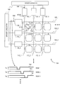
- FIG. 1 shows a circuit schematic of part of an integrated circuit device having a phase-change memory array in which the variation in cell voltage has been reduced.
- FIG. 2 illustrates a circuit schematic of an integrated circuit device featuring a phase-change memory array in which lumped resistors are used to help reduce the variation in cell voltage across the array.
- FIG. 3 depicts a circuit schematic of an integrated circuit device featuring a phase-change memory array, wherein driver strength varies as a function of the bitline or wordline being driven.
- FIG. 4 depicts a flow diagram of a process for designing the integrated circuit device having a phase-change memory array with reduced cell voltage variation.
- An integrated circuit device having a number of bitlines and wordlines, and a number of memory cells each of which has a structural phase-change material to store the cell's data. Each cell is coupled between a corresponding bitline-wordline pair. Techniques are described for reducing the variation in cell voltage across the cells of the array as a programming pulse is applied to each bitline-wordline pair. The reduction in the variation of cell voltage helps obtain more uniform programming conditions which lead to a greater likelihood of error free programming of the memory array.
- FIG. 1 what's shown is a circuit schematic of part of an integrated circuit device 104 having a phase-change memory array in which the variation in cell voltage during programming has been reduced.
- the array has a number of vertically oriented conductive lines 112 _ 1 , 112 _ 2 , . . . (referred to here as bitlines) and a number of horizontally oriented conductive lines 108 _ 1 , 108 _ 2 , . . . (called wordlines) arranged in a cross-point matrix as shown.
- This matrix arrangement allows each crossing of a bitline-wordline pair to be associated with a separate memory cell 114 formed nearby within a substrate of the integrated circuit device 104 .
- every cell 114 in the array may be designed to have the same structure.
- the cells are now described using only a representative cell, where it is clear that the following description applies to all other cells in the array.
- the cell 114 has a small volume of structural phase-change material 118 that is coupled in series with a diode structure 124 and a matching resistor 120 .
- the volume of phase-change material 118 acts as a programmable resistor and changes from one resistivity state to another, corresponding to a change from one type of structure to another, when an appropriately sized pulse of current has passed through it.
- the series coupled components in the cell 114 can be accessed through terminals 1 and 2 of the cell 114 , where the first terminal is coupled to a bitline 112 while the second terminal is coupled to a wordline 108 which form the corresponding bitline-wordline pair for this cell.
- the integrated circuit device 104 is equipped with a number of bitline compensation elements 132 _ 1 , 132 _ 2 . . . each being coupled in series with a separate one of the bitlines 112 .
- the device 104 has a number of wordline compensation elements 128 _ 1 , 128 _ 2 . . . each being coupled in series with a separate one of the wordlines 108 .
- Each of these compensation elements has a resistance that together are designed to minimize the variation in cell voltage across the array.
- This technique overcomes the large variation in resistance that is exhibited between bitline-wordline pairs that are located far from each other in the array.
- FIG. 1 shows the distributed resistance of the bitlines and wordlines as resistor symbols in dotted lines. An equivalent resistance 116 in dotted lines is drawn between each adjacent pair of cell terminal connections to a wordline or bitline to represent this distributed resistance.
- the bitline and wordline compensation elements 132 , 128 have resistances such that a sum of (1) the resistance along the corresponding bitline 112 of a cell 114 between a first terminal of the cell 114 and a far terminal of the bitline compensation element 132 that is coupled to the corresponding bitline 112 and (2) the resistance along the corresponding wordline 108 of the cell 114 between a second terminal of the cell 114 and a far terminal of the wordline compensation element 128 that is coupled to the corresponding wordline 108 , is essentially equal for each of the memory cells.
- This is an ideal situation which may not be met in practice, such that rather than having that sum be essentially equal, it may be more practical to have variation in that sum be minimized across the cells of the array.
- variation in cell voltage across the cells may be reduced when the same programming voltage pulse 150 (having a magnitude V p ) as shown is applied to each bitline-wordline pair by driver circuitry 140 . More specifically, the same voltage pulse 150 can be applied directly to the far terminal of each wordline compensation element 128 while at the same time being able to minimize the variation in cell voltage across terminals 1 and 2 of each cell 114 in the array. This occurs because the total resistance between the far terminal of the wordline compensation element 128 and the far terminal of the corresponding bitline compensation element 132 is designed to be the same, for each memory cell that is accessed by a corresponding bitline-wordline pair.
- FIG. 2 what is shown is a circuit schematic of an alternative embodiment of the cell voltage variation reduction technique, as part of an integrated circuit device 204 .
- This device 204 features driver circuitry 240 which directly drives the same programming voltage pulse 250 on each wordline 108 , where in this embodiment the pulse 250 is ‘active high’ rather than active low as in the pulse 150 . That is because in this embodiment, the diode structure 124 in each memory cell 214 has been reversed, so that its forward current is now directed in the opposite direction than in the cell 114 of FIG. 1 .
- FIG. 2 also shows an embodiment in which each bitline compensation element is a lumped, passive resistor 232 , and each wordline compensation element is a lumped, passive resistor 228 .
- This mechanism for cell voltage variation reduction is similar to the more general version in FIG.
- lumped resistors 232 R B1 >R B2 >R B3. . .
- lumped resistors 228 R W1 >R W2 >R W3. . .
- the difference in resistance between adjacent lumped resistors 232 that are coupled to the bitlines 112 is essentially the resistance between a second terminal of a memory cell 214 that is coupled to the selected bitline-wordline pair and a second terminal of a memory cell coupled to the immediately adjacent bitline-wordline pair along the selected wordline.
- the difference in resistance between lumped resistors 232 _ 1 (R B1 ) and 232 _ 2 (R B2 ) would be the equivalent resistance 260 , where R B1 is larger than R B2 by an amount essentially equal to the equivalent resistance 260 .
- R B2 is larger than R B3 by the equivalent resistance 270 , and so on.
- R W1 is greater than R W2 by an amount essentially equal to the equivalent resistance 280 .
- FIG. 3 what is shown is another embodiment of the cell voltage variation reduction technique in an integrated circuit device 304 in which wordline driver circuitry 340 cooperates with bitline driver circuitry 342 to provide not the same programming voltage pulse but rather a variable strength (voltage) programming pulse.
- the magnitude of the pulse varies as a function of the bitline-wordline pair to which the pulse is being applied so as to compensate for the buildup of distributed resistance in the array.
- the strength or maximum voltage of the programming pulse is greater if the bitline-wordline pair to which the pulse is being applied is located further from the driver circuitry.
- FIG. 4 shows a flow diagram of operations for designing an integrated circuit device in which the variation in cell voltage (across a phase-change memory array) during programming can be minimized.
- the process begins with the creation of a representation of a number of bitlines and wordlines that are to be built into the device to form the memory array (operation 404 ). This representation may be created using a computer aided design system for designing and simulating electronic devices. Each bitline and wordline is assigned equivalent resistances that may be based on a common distributed resistance model of a conductive line.
- the process also includes creating a representation of a number of memory cells that form the array and are built into the integrated circuit.
- Each cell is to have a structural phase-change material to store the cells' data, and to be coupled between a corresponding bitline-wordline pair, with a given total cell resistance (operation 408 ).
- a representation of a number of bitline compensation elements and wordline compensation elements as described above is created, where these elements are to be built into the integrated circuit such that each element is coupled in series with a separate one of the bitlines and each wordline element is to be coupled in series with a separate one of the wordlines (operation 412 ).
- these compensation elements may include various circuit elements, including for instance a single lumped resistor, with resistances selected so that variation in the following sum resistance is minimized for each of the memory cells:
- the resistance of a bitline compensation element of each selected bitline-wordline pair is selected to be smaller than a resistance of the compensation element of an immediately adjacent bitline-wordline pair, and wherein this resistance is smaller by an amount essentially equal to the resistance between a terminal of a memory cell coupled to the selected bitline-wordline pair and a second terminal of another memory cell coupled to an immediately adjacent bitline-wordline pair, along the selected wordline.
- the same type of continuously decreasing resistances can be provided for the wordline compensation elements.
- the programming of the array is simulated, by representing the application of the same voltage pulse to each bitline-wordline pair (via the corresponding compensation elements), to determine whether the variation in cell voltage has been minimized across the cells of the array. (operation 416 ). This would include creating a representation of the driver circuitry (see e.g. FIGS. 1-3) such that the driver circuitry is coupled to apply to each bitline-wordline pair a programming pulse having the same voltage magnitude.
- phase-change memory array includes decoding logic that translates address information and data information into the appropriate pulses that are applied to the selected bitline-wordline pairs.
- decoding logic that translates address information and data information into the appropriate pulses that are applied to the selected bitline-wordline pairs.
- the above description may refer to a single cell being programmed, the concepts are also applicable to simultaneously program a number of cells.
- the compensation elements may include active devices which are designed to operate in such a manner that the variation in total resistance that is presented to driver circuitry across each bitline-wordline pair is minimized.
Abstract
Description
Claims (15)
Priority Applications (1)
| Application Number | Priority Date | Filing Date | Title |
|---|---|---|---|
| US09/881,439 US6480438B1 (en) | 2001-06-12 | 2001-06-12 | Providing equal cell programming conditions across a large and high density array of phase-change memory cells |
Applications Claiming Priority (1)
| Application Number | Priority Date | Filing Date | Title |
|---|---|---|---|
| US09/881,439 US6480438B1 (en) | 2001-06-12 | 2001-06-12 | Providing equal cell programming conditions across a large and high density array of phase-change memory cells |
Publications (1)
| Publication Number | Publication Date |
|---|---|
| US6480438B1 true US6480438B1 (en) | 2002-11-12 |
Family
ID=25378486
Family Applications (1)
| Application Number | Title | Priority Date | Filing Date |
|---|---|---|---|
| US09/881,439 Expired - Lifetime US6480438B1 (en) | 2001-06-12 | 2001-06-12 | Providing equal cell programming conditions across a large and high density array of phase-change memory cells |
Country Status (1)
| Country | Link |
|---|---|
| US (1) | US6480438B1 (en) |
Cited By (84)
| Publication number | Priority date | Publication date | Assignee | Title |
|---|---|---|---|---|
| US20030096497A1 (en) * | 2001-11-19 | 2003-05-22 | Micron Technology, Inc. | Electrode structure for use in an integrated circuit |
| US6633178B2 (en) | 2001-09-28 | 2003-10-14 | Intel Corporation | Apparatus and method for power efficient line driver |
| US20030198118A1 (en) * | 2001-08-02 | 2003-10-23 | Lowery Tyler A. | Method for reading a structural phase-change memory |
| US20030206428A1 (en) * | 2002-05-01 | 2003-11-06 | Ward Parkinson | High voltage row and column driver for programmable resistance memory |
| US20040053461A1 (en) * | 2002-08-29 | 2004-03-18 | Moore John T. | Graded GexSe100-x concentration in PCRAM |
| US20040170053A1 (en) * | 2003-02-28 | 2004-09-02 | Keun-Ho Lee | Phase change memory array |
| US6791885B2 (en) | 2002-02-19 | 2004-09-14 | Micron Technology, Inc. | Programmable conductor random access memory and method for sensing same |
| US6809362B2 (en) | 2002-02-20 | 2004-10-26 | Micron Technology, Inc. | Multiple data state memory cell |
| US20040211957A1 (en) * | 2002-08-29 | 2004-10-28 | Moore John T. | Method and apparatus for controlling metal doping of a chalcogenide memory element |
| US6812087B2 (en) | 2002-01-31 | 2004-11-02 | Micron Technology, Inc. | Methods of forming non-volatile resistance variable devices and methods of forming silver selenide comprising structures |
| US6813178B2 (en) | 2003-03-12 | 2004-11-02 | Micron Technology, Inc. | Chalcogenide glass constant current device, and its method of fabrication and operation |
| US6833559B2 (en) | 2001-02-08 | 2004-12-21 | Micron Technology, Inc. | Non-volatile resistance variable device |
| US20040264234A1 (en) * | 2003-06-25 | 2004-12-30 | Moore John T. | PCRAM cell operation method to control on/off resistance variation |
| US6864521B2 (en) | 2002-08-29 | 2005-03-08 | Micron Technology, Inc. | Method to control silver concentration in a resistance variable memory element |
| EP1513161A2 (en) | 2003-09-03 | 2005-03-09 | Sharp Kabushiki Kaisha | Semiconductor memory device |
| US6878569B2 (en) * | 2001-03-15 | 2005-04-12 | Micron Technology, Inc. | Agglomeration elimination for metal sputter deposition of chalcogenides |
| US6888155B2 (en) | 2001-08-30 | 2005-05-03 | Micron Technology, Inc. | Stoichiometry for chalcogenide glasses useful for memory devices and method of formation |
| US20050122771A1 (en) * | 2003-12-05 | 2005-06-09 | Bomy Chen | Memory device and method of operating same |
| US20050162907A1 (en) * | 2004-01-28 | 2005-07-28 | Campbell Kristy A. | Resistance variable memory elements based on polarized silver-selenide network growth |
| US20050169093A1 (en) * | 2004-02-04 | 2005-08-04 | Byung-Gil Choi | Phase-change memory device and method of writing a phase-change memory device |
| US20050185480A1 (en) * | 2004-02-19 | 2005-08-25 | Anoop Mukker | Dynamically activated memory controller data termination |
| US20050185444A1 (en) * | 2004-02-25 | 2005-08-25 | Soo-Guil Yang | Phase-changeable memory device and method of manufacturing the same |
| US6939744B2 (en) | 1996-05-21 | 2005-09-06 | Micron Technology, Inc. | Use of palladium in IC manufacturing with conductive polymer bump |
| US6961277B2 (en) | 2003-07-08 | 2005-11-01 | Micron Technology, Inc. | Method of refreshing a PCRAM memory device |
| EP1617437A1 (en) * | 2004-07-09 | 2006-01-18 | Samsung Electronics Co, Ltd | Phase change memory device and programming and controlling methods |
| US20060120148A1 (en) * | 2004-10-26 | 2006-06-08 | Samsung Electronics Co., Ltd. | Semiconductor memory device with stacked memory cell and method of manufacturing the stacked memory cell |
| US7105864B2 (en) | 2004-01-29 | 2006-09-12 | Micron Technology, Inc. | Non-volatile zero field splitting resonance memory |
| US20060215440A1 (en) * | 2005-03-24 | 2006-09-28 | Beak-Hyung Cho | Nonvolatile memory devices having enhanced bit line and/or word line driving capability |
| US20060220071A1 (en) * | 2005-04-04 | 2006-10-05 | Kang Sang-Beom | Phase-change semiconductor memory device and method of programming the same |
| US20060274574A1 (en) * | 2004-02-04 | 2006-12-07 | Byung-Gil Choi | Phase-change memory device and method of writing a phase-change memory device |
| US20070091665A1 (en) * | 2005-10-15 | 2007-04-26 | Hyung-Rok Oh | Phase change random access memory and method of controlling read operation thereof |
| US20070133269A1 (en) * | 2005-12-14 | 2007-06-14 | Kwang-Jin Lee | Non-volatile memory devices and systems including phase-change one-time-programmable (OTP) memory cells and related methods |
| US20070230240A1 (en) * | 2006-03-31 | 2007-10-04 | Byung-Gil Choi | Phase change memory device and related programming method |
| US20070230239A1 (en) * | 2006-03-31 | 2007-10-04 | Byung-Gil Choi | Phase change memory devices and program methods |
| US7307908B2 (en) | 2002-08-29 | 2007-12-11 | Micron Technology, Inc. | Software refreshed memory device and method |
| US7348205B2 (en) | 2001-08-29 | 2008-03-25 | Micron Technology, Inc. | Method of forming resistance variable devices |
| EP1906411A1 (en) | 2006-09-27 | 2008-04-02 | Samsung Electronics Co., Ltd. | Method of programming a phase change memory device |
| US20080084734A1 (en) * | 2006-10-06 | 2008-04-10 | De Brosse John K | Balanced and bi-directional bit line paths for memory arrays with programmable memory cells |
| US20080165574A1 (en) * | 2007-01-08 | 2008-07-10 | Samsung Electronics Co., Ltd. | Memory device including thermal conductor located between progammable volumes |
| US20090109788A1 (en) * | 2007-10-31 | 2009-04-30 | Samsung Electronics Co., Ltd. | Data management method and mapping table update method in non-volatile memory device |
| US20090129195A1 (en) * | 2007-11-15 | 2009-05-21 | De Brosse John K | Balanced and bi-directional bit line paths for memory arrays with programmable memory cells |
| US20090154221A1 (en) * | 2007-12-14 | 2009-06-18 | Samsung Electronics Co., Ltd. | Non-Volatile memory device using variable resistance element with an improved write performance |
| US20090168493A1 (en) * | 2004-10-26 | 2009-07-02 | Samsung Electronics Co., Ltd | Semiconductor memory device with stacked memory cell and method of manufacturing the stacked memory cell |
| DE102006030749B4 (en) * | 2005-06-22 | 2009-11-12 | Samsung Electronics Co., Ltd., Suwon | Phase change memory device with word line drivers |
| DE102006052397B4 (en) * | 2005-11-07 | 2009-12-31 | Samsung Electronics Co., Ltd., Suwon | Non-volatile semiconductor memory, nonvolatile semiconductor memory device, method of reading a phase change memory cell and system |
| US7663137B2 (en) | 2005-08-02 | 2010-02-16 | Micron Technology, Inc. | Phase change memory cell and method of formation |
| US7663133B2 (en) | 2005-04-22 | 2010-02-16 | Micron Technology, Inc. | Memory elements having patterned electrodes and method of forming the same |
| US7668000B2 (en) | 2005-08-15 | 2010-02-23 | Micron Technology, Inc. | Method and apparatus providing a cross-point memory array using a variable resistance memory cell and capacitance |
| US7682992B2 (en) | 2004-08-12 | 2010-03-23 | Micron Technology, Inc. | Resistance variable memory with temperature tolerant materials |
| US7687793B2 (en) | 2001-05-11 | 2010-03-30 | Micron Technology, Inc. | Resistance variable memory cells |
| US7701760B2 (en) | 2005-08-01 | 2010-04-20 | Micron Technology, Inc. | Resistance variable memory device with sputtered metal-chalcogenide region and method of fabrication |
| US7700422B2 (en) | 2005-04-22 | 2010-04-20 | Micron Technology, Inc. | Methods of forming memory arrays for increased bit density |
| US7709885B2 (en) | 2005-08-09 | 2010-05-04 | Micron Technology, Inc. | Access transistor for memory device |
| US7723713B2 (en) | 2002-02-20 | 2010-05-25 | Micron Technology, Inc. | Layered resistance variable memory device and method of fabrication |
| US20100128516A1 (en) * | 2008-11-26 | 2010-05-27 | Samsung Electronics Co., Ltd. | Nonvolatile Memory Devices Having Bit Line Discharge Control Circuits Therein that Provide Equivalent Bit Line Discharge Control |
| US20100128512A1 (en) * | 2005-11-02 | 2010-05-27 | Tetsuya Ohnishi | Semiconductor memory device having cross-point structure |
| US7745808B2 (en) | 2003-04-10 | 2010-06-29 | Micron Technology, Inc. | Differential negative resistance memory |
| US7749853B2 (en) | 2004-07-19 | 2010-07-06 | Microntechnology, Inc. | Method of forming a variable resistance memory device comprising tin selenide |
| DE102006042621B4 (en) * | 2005-09-08 | 2010-07-29 | Samsung Electronics Co., Ltd., Suwon | Phase change memory device |
| US7785976B2 (en) | 2004-08-12 | 2010-08-31 | Micron Technology, Inc. | Method of forming a memory device incorporating a resistance-variable chalcogenide element |
| US7791058B2 (en) | 2006-08-29 | 2010-09-07 | Micron Technology, Inc. | Enhanced memory density resistance variable memory cells, arrays, devices and systems including the same, and methods of fabrication |
| EP2240935A1 (en) * | 2007-12-10 | 2010-10-20 | Kabushiki Kaisha Toshiba | Semiconductor memory device and memory cell voltage application method |
| US7869249B2 (en) | 2001-11-20 | 2011-01-11 | Micron Technology, Inc. | Complementary bit PCRAM sense amplifier and method of operation |
| US7879646B2 (en) | 2002-07-10 | 2011-02-01 | Micron Technology, Inc. | Assemblies displaying differential negative resistance, semiconductor constructions, and methods of forming assemblies displaying differential negative resistance |
| US7910397B2 (en) | 2004-12-22 | 2011-03-22 | Micron Technology, Inc. | Small electrode for resistance variable devices |
| US7964436B2 (en) | 2002-06-06 | 2011-06-21 | Round Rock Research, Llc | Co-sputter deposition of metal-doped chalcogenides |
| US20110222330A1 (en) * | 2010-03-11 | 2011-09-15 | Samsung Electronics Co., Ltd. | Nonvolatile memory device comprising one-time-programmable lock bit register |
| US8101936B2 (en) | 2005-02-23 | 2012-01-24 | Micron Technology, Inc. | SnSe-based limited reprogrammable cell |
| US8467236B2 (en) | 2008-08-01 | 2013-06-18 | Boise State University | Continuously variable resistor |
| US8619485B2 (en) | 2004-03-10 | 2013-12-31 | Round Rock Research, Llc | Power management control and controlling memory refresh operations |
| US8624215B2 (en) | 2005-12-20 | 2014-01-07 | University Of Southampton | Phase change memory devices and methods comprising gallium, lanthanide and chalcogenide compounds |
| US8964488B2 (en) | 2007-12-14 | 2015-02-24 | Samsung Electronics Co., Ltd. | Non-volatile memory device using variable resistance element with an improved write performance |
| US9165646B2 (en) | 2012-10-08 | 2015-10-20 | Samsung Electronics Co., Ltd. | Resistive memory device including compensation resistive device and method of compensating resistance distribution |
| US9183931B2 (en) | 2013-12-03 | 2015-11-10 | Samsung Electronics Co., Ltd. | Resistive memory device capable of increasing sensing margin by controlling interface states of cell transistors |
| WO2016025374A1 (en) * | 2010-09-01 | 2016-02-18 | Nantero Inc. | Method for dynamically accessing and programming resistive change element arrays |
| US9552986B2 (en) | 2002-08-29 | 2017-01-24 | Micron Technology, Inc. | Forming a memory device using sputtering to deposit silver-selenide film |
| KR20170042640A (en) * | 2014-08-12 | 2017-04-19 | 난테로 인크. | Method for dynamically accessing and programming resistive change element arrays |
| US20190088289A1 (en) * | 2017-09-15 | 2019-03-21 | Toshiba Memory Corporation | Semiconductor memory device |
| US10290349B2 (en) | 2015-07-29 | 2019-05-14 | Nantero, Inc. | DDR compatible open array architectures for resistive change element arrays |
| US10340005B2 (en) | 2015-07-29 | 2019-07-02 | Nantero, Inc. | Resistive change element arrays with in situ initialization |
| US10949132B1 (en) | 2019-09-19 | 2021-03-16 | Kioxia Corporation | Semiconductor storage device |
| US11043268B2 (en) * | 2019-07-16 | 2021-06-22 | Samsung Electronics Co., Ltd. | Resistive memory devices and methods of operating resistive memory devices including adjustment of current path resistance of a selected memory cell in a resistive memory device |
| US20210358545A1 (en) * | 2020-05-13 | 2021-11-18 | Micron Technology, Inc. | Passive compensation for electrical distance |
| US11322206B2 (en) | 2019-11-28 | 2022-05-03 | Samsung Electronics Co., Ltd. | Storage device and operating method thereof |
Citations (6)
| Publication number | Priority date | Publication date | Assignee | Title |
|---|---|---|---|---|
| US3271591A (en) | 1963-09-20 | 1966-09-06 | Energy Conversion Devices Inc | Symmetrical current controlling device |
| US3530441A (en) | 1969-01-15 | 1970-09-22 | Energy Conversion Devices Inc | Method and apparatus for storing and retrieving information |
| US4529896A (en) * | 1982-03-24 | 1985-07-16 | International Business Machines Corporation | True/complement generator employing feedback circuit means for controlling the switching of the outputs |
| US6085341A (en) | 1996-12-31 | 2000-07-04 | Intel Corporation | Memory test mode for wordline resistive defects |
| US6141241A (en) | 1998-06-23 | 2000-10-31 | Energy Conversion Devices, Inc. | Universal memory element with systems employing same and apparatus and method for reading, writing and programming same |
| US20010047449A1 (en) * | 1994-01-20 | 2001-11-29 | Tomohisa Wada | Semiconductor memory device and computer having a synchronization signal indicating that the memory data output is valid |
-
2001
- 2001-06-12 US US09/881,439 patent/US6480438B1/en not_active Expired - Lifetime
Patent Citations (6)
| Publication number | Priority date | Publication date | Assignee | Title |
|---|---|---|---|---|
| US3271591A (en) | 1963-09-20 | 1966-09-06 | Energy Conversion Devices Inc | Symmetrical current controlling device |
| US3530441A (en) | 1969-01-15 | 1970-09-22 | Energy Conversion Devices Inc | Method and apparatus for storing and retrieving information |
| US4529896A (en) * | 1982-03-24 | 1985-07-16 | International Business Machines Corporation | True/complement generator employing feedback circuit means for controlling the switching of the outputs |
| US20010047449A1 (en) * | 1994-01-20 | 2001-11-29 | Tomohisa Wada | Semiconductor memory device and computer having a synchronization signal indicating that the memory data output is valid |
| US6085341A (en) | 1996-12-31 | 2000-07-04 | Intel Corporation | Memory test mode for wordline resistive defects |
| US6141241A (en) | 1998-06-23 | 2000-10-31 | Energy Conversion Devices, Inc. | Universal memory element with systems employing same and apparatus and method for reading, writing and programming same |
Cited By (168)
| Publication number | Priority date | Publication date | Assignee | Title |
|---|---|---|---|---|
| US6939744B2 (en) | 1996-05-21 | 2005-09-06 | Micron Technology, Inc. | Use of palladium in IC manufacturing with conductive polymer bump |
| US6833559B2 (en) | 2001-02-08 | 2004-12-21 | Micron Technology, Inc. | Non-volatile resistance variable device |
| US6878569B2 (en) * | 2001-03-15 | 2005-04-12 | Micron Technology, Inc. | Agglomeration elimination for metal sputter deposition of chalcogenides |
| US7687793B2 (en) | 2001-05-11 | 2010-03-30 | Micron Technology, Inc. | Resistance variable memory cells |
| US20030198118A1 (en) * | 2001-08-02 | 2003-10-23 | Lowery Tyler A. | Method for reading a structural phase-change memory |
| US6707712B2 (en) * | 2001-08-02 | 2004-03-16 | Intel Corporation | Method for reading a structural phase-change memory |
| US7863597B2 (en) | 2001-08-29 | 2011-01-04 | Micron Technology, Inc. | Resistance variable memory devices with passivating material |
| US7348205B2 (en) | 2001-08-29 | 2008-03-25 | Micron Technology, Inc. | Method of forming resistance variable devices |
| US6888155B2 (en) | 2001-08-30 | 2005-05-03 | Micron Technology, Inc. | Stoichiometry for chalcogenide glasses useful for memory devices and method of formation |
| US6633178B2 (en) | 2001-09-28 | 2003-10-14 | Intel Corporation | Apparatus and method for power efficient line driver |
| US20040051555A1 (en) * | 2001-09-28 | 2004-03-18 | Wilcox Jeffrey R. | Apparatus and method for power efficient line driver |
| US6970010B2 (en) | 2001-09-28 | 2005-11-29 | Intel Corporation | Apparatus and method for power efficient line driver |
| US20030096497A1 (en) * | 2001-11-19 | 2003-05-22 | Micron Technology, Inc. | Electrode structure for use in an integrated circuit |
| US6815818B2 (en) * | 2001-11-19 | 2004-11-09 | Micron Technology, Inc. | Electrode structure for use in an integrated circuit |
| US7869249B2 (en) | 2001-11-20 | 2011-01-11 | Micron Technology, Inc. | Complementary bit PCRAM sense amplifier and method of operation |
| US6812087B2 (en) | 2002-01-31 | 2004-11-02 | Micron Technology, Inc. | Methods of forming non-volatile resistance variable devices and methods of forming silver selenide comprising structures |
| US6791885B2 (en) | 2002-02-19 | 2004-09-14 | Micron Technology, Inc. | Programmable conductor random access memory and method for sensing same |
| US7723713B2 (en) | 2002-02-20 | 2010-05-25 | Micron Technology, Inc. | Layered resistance variable memory device and method of fabrication |
| US6809362B2 (en) | 2002-02-20 | 2004-10-26 | Micron Technology, Inc. | Multiple data state memory cell |
| US8263958B2 (en) | 2002-02-20 | 2012-09-11 | Micron Technology, Inc. | Layered resistance variable memory device and method of fabrication |
| US6781860B2 (en) * | 2002-05-01 | 2004-08-24 | Ovonyx, Inc. | High voltage row and column driver for programmable resistance memory |
| WO2003094201A3 (en) * | 2002-05-01 | 2004-04-29 | Ovonyx Inc | High voltage row and column driver for programmable resistance memory |
| WO2003094201A2 (en) * | 2002-05-01 | 2003-11-13 | Ovonyx,Inc. | High voltage row and column driver for programmable resistance memory |
| US20030206428A1 (en) * | 2002-05-01 | 2003-11-06 | Ward Parkinson | High voltage row and column driver for programmable resistance memory |
| US7964436B2 (en) | 2002-06-06 | 2011-06-21 | Round Rock Research, Llc | Co-sputter deposition of metal-doped chalcogenides |
| US7879646B2 (en) | 2002-07-10 | 2011-02-01 | Micron Technology, Inc. | Assemblies displaying differential negative resistance, semiconductor constructions, and methods of forming assemblies displaying differential negative resistance |
| US6856002B2 (en) | 2002-08-29 | 2005-02-15 | Micron Technology, Inc. | Graded GexSe100-x concentration in PCRAM |
| US6864521B2 (en) | 2002-08-29 | 2005-03-08 | Micron Technology, Inc. | Method to control silver concentration in a resistance variable memory element |
| US20050148150A1 (en) * | 2002-08-29 | 2005-07-07 | Moore John T. | Memory element and its method of formation |
| US20040053461A1 (en) * | 2002-08-29 | 2004-03-18 | Moore John T. | Graded GexSe100-x concentration in PCRAM |
| US7518212B2 (en) | 2002-08-29 | 2009-04-14 | Micron Technology, Inc. | Graded GexSe100-x concentration in PCRAM |
| US7564731B2 (en) | 2002-08-29 | 2009-07-21 | Micron Technology, Inc. | Software refreshed memory device and method |
| US7768861B2 (en) | 2002-08-29 | 2010-08-03 | Micron Technology, Inc. | Software refreshed memory device and method |
| US6953720B2 (en) | 2002-08-29 | 2005-10-11 | Micron Technology, Inc. | Methods for forming chalcogenide glass-based memory elements |
| US7692177B2 (en) | 2002-08-29 | 2010-04-06 | Micron Technology, Inc. | Resistance variable memory element and its method of formation |
| US20040211957A1 (en) * | 2002-08-29 | 2004-10-28 | Moore John T. | Method and apparatus for controlling metal doping of a chalcogenide memory element |
| US7223627B2 (en) | 2002-08-29 | 2007-05-29 | Micron Technology, Inc. | Memory element and its method of formation |
| US9552986B2 (en) | 2002-08-29 | 2017-01-24 | Micron Technology, Inc. | Forming a memory device using sputtering to deposit silver-selenide film |
| US7944768B2 (en) | 2002-08-29 | 2011-05-17 | Micron Technology, Inc. | Software refreshed memory device and method |
| US7307908B2 (en) | 2002-08-29 | 2007-12-11 | Micron Technology, Inc. | Software refreshed memory device and method |
| US6862214B2 (en) * | 2003-02-28 | 2005-03-01 | Samsung Electronics Co., Ltd. | Phase change memory array |
| US20040170053A1 (en) * | 2003-02-28 | 2004-09-02 | Keun-Ho Lee | Phase change memory array |
| US6813178B2 (en) | 2003-03-12 | 2004-11-02 | Micron Technology, Inc. | Chalcogenide glass constant current device, and its method of fabrication and operation |
| US7745808B2 (en) | 2003-04-10 | 2010-06-29 | Micron Technology, Inc. | Differential negative resistance memory |
| US20040264234A1 (en) * | 2003-06-25 | 2004-12-30 | Moore John T. | PCRAM cell operation method to control on/off resistance variation |
| US6961277B2 (en) | 2003-07-08 | 2005-11-01 | Micron Technology, Inc. | Method of refreshing a PCRAM memory device |
| EP1513161A3 (en) * | 2003-09-03 | 2006-11-22 | Sharp Kabushiki Kaisha | Semiconductor memory device |
| EP1513161A2 (en) | 2003-09-03 | 2005-03-09 | Sharp Kabushiki Kaisha | Semiconductor memory device |
| CN1591692B (en) * | 2003-09-03 | 2013-06-12 | 异基因开发有限责任公司 | Semiconductor memory device |
| US20050122771A1 (en) * | 2003-12-05 | 2005-06-09 | Bomy Chen | Memory device and method of operating same |
| US6937507B2 (en) | 2003-12-05 | 2005-08-30 | Silicon Storage Technology, Inc. | Memory device and method of operating same |
| US7153721B2 (en) | 2004-01-28 | 2006-12-26 | Micron Technology, Inc. | Resistance variable memory elements based on polarized silver-selenide network growth |
| US20050286294A1 (en) * | 2004-01-28 | 2005-12-29 | Campbell Kristy A | Resistance variable memory elements based on polarized silver-selenide network growth |
| US20050162907A1 (en) * | 2004-01-28 | 2005-07-28 | Campbell Kristy A. | Resistance variable memory elements based on polarized silver-selenide network growth |
| US7105864B2 (en) | 2004-01-29 | 2006-09-12 | Micron Technology, Inc. | Non-volatile zero field splitting resonance memory |
| US7110286B2 (en) | 2004-02-04 | 2006-09-19 | Samsung Electronics Co., Ltd. | Phase-change memory device and method of writing a phase-change memory device |
| US20060274574A1 (en) * | 2004-02-04 | 2006-12-07 | Byung-Gil Choi | Phase-change memory device and method of writing a phase-change memory device |
| US20050169093A1 (en) * | 2004-02-04 | 2005-08-04 | Byung-Gil Choi | Phase-change memory device and method of writing a phase-change memory device |
| US7502251B2 (en) | 2004-02-04 | 2009-03-10 | Samsung Electronics Co., Ltd. | Phase-change memory device and method of writing a phase-change memory device |
| US7009894B2 (en) | 2004-02-19 | 2006-03-07 | Intel Corporation | Dynamically activated memory controller data termination |
| US20050185480A1 (en) * | 2004-02-19 | 2005-08-25 | Anoop Mukker | Dynamically activated memory controller data termination |
| US20080026535A1 (en) * | 2004-02-25 | 2008-01-31 | Soo-Guil Yang | Phase-changeable memory device and method of manufacturing the same |
| US20050185444A1 (en) * | 2004-02-25 | 2005-08-25 | Soo-Guil Yang | Phase-changeable memory device and method of manufacturing the same |
| US7700430B2 (en) | 2004-02-25 | 2010-04-20 | Samsung Electronics Co., Ltd. | Phase-changeable memory device and method of manufacturing the same |
| US7295463B2 (en) | 2004-02-25 | 2007-11-13 | Samsung Electronics Co., Ltd. | Phase-changeable memory device and method of manufacturing the same |
| US8619485B2 (en) | 2004-03-10 | 2013-12-31 | Round Rock Research, Llc | Power management control and controlling memory refresh operations |
| US9142263B2 (en) | 2004-03-10 | 2015-09-22 | Round Rock Research, Llc | Power management control and controlling memory refresh operations |
| US7643335B2 (en) | 2004-07-09 | 2010-01-05 | Samsung Electronics Co., Ltd. | Apparatus and systems using phase change memories |
| US20100097850A1 (en) * | 2004-07-09 | 2010-04-22 | Samsung Electronics Co., Ltd. | Apparatus and systems using phase change memories |
| EP1617437A1 (en) * | 2004-07-09 | 2006-01-18 | Samsung Electronics Co, Ltd | Phase change memory device and programming and controlling methods |
| CN1734671B (en) * | 2004-07-09 | 2010-04-21 | 三星电子株式会社 | Phase change memories and/or methods of programming phase change memories using sequential reset control |
| US7944741B2 (en) | 2004-07-09 | 2011-05-17 | Samsung Electronics Co., Ltd. | Apparatus and systems using phase change memories |
| JP2006024355A (en) * | 2004-07-09 | 2006-01-26 | Samsung Electronics Co Ltd | Phase change memory device and programming method |
| US20080137402A1 (en) * | 2004-07-09 | 2008-06-12 | Samsung Electronics Co., Ltd. | Apparatus and systems using phase change memories |
| US8194442B2 (en) | 2004-07-09 | 2012-06-05 | Samsung Electronics Co., Ltd. | Apparatus and systems using phase change memories |
| US7304885B2 (en) | 2004-07-09 | 2007-12-04 | Samsung Electronics Co., Ltd. | Phase change memories and/or methods of programming phase change memories using sequential reset control |
| US7749853B2 (en) | 2004-07-19 | 2010-07-06 | Microntechnology, Inc. | Method of forming a variable resistance memory device comprising tin selenide |
| US7759665B2 (en) | 2004-07-19 | 2010-07-20 | Micron Technology, Inc. | PCRAM device with switching glass layer |
| US7994491B2 (en) | 2004-08-12 | 2011-08-09 | Micron Technology, Inc. | PCRAM device with switching glass layer |
| US8334186B2 (en) | 2004-08-12 | 2012-12-18 | Micron Technology, Inc. | Method of forming a memory device incorporating a resistance variable chalcogenide element |
| US7924603B2 (en) | 2004-08-12 | 2011-04-12 | Micron Technology, Inc. | Resistance variable memory with temperature tolerant materials |
| US7785976B2 (en) | 2004-08-12 | 2010-08-31 | Micron Technology, Inc. | Method of forming a memory device incorporating a resistance-variable chalcogenide element |
| US8895401B2 (en) | 2004-08-12 | 2014-11-25 | Micron Technology, Inc. | Method of forming a memory device incorporating a resistance variable chalcogenide element |
| US7682992B2 (en) | 2004-08-12 | 2010-03-23 | Micron Technology, Inc. | Resistance variable memory with temperature tolerant materials |
| US8487288B2 (en) | 2004-08-12 | 2013-07-16 | Micron Technology, Inc. | Memory device incorporating a resistance variable chalcogenide element |
| US8179711B2 (en) | 2004-10-26 | 2012-05-15 | Samsung Electronics Co., Ltd. | Semiconductor memory device with stacked memory cell and method of manufacturing the stacked memory cell |
| US20090168493A1 (en) * | 2004-10-26 | 2009-07-02 | Samsung Electronics Co., Ltd | Semiconductor memory device with stacked memory cell and method of manufacturing the stacked memory cell |
| US20060120148A1 (en) * | 2004-10-26 | 2006-06-08 | Samsung Electronics Co., Ltd. | Semiconductor memory device with stacked memory cell and method of manufacturing the stacked memory cell |
| US7453716B2 (en) | 2004-10-26 | 2008-11-18 | Samsung Electronics Co., Ltd | Semiconductor memory device with stacked control transistors |
| US7910397B2 (en) | 2004-12-22 | 2011-03-22 | Micron Technology, Inc. | Small electrode for resistance variable devices |
| US8101936B2 (en) | 2005-02-23 | 2012-01-24 | Micron Technology, Inc. | SnSe-based limited reprogrammable cell |
| US7397681B2 (en) | 2005-03-24 | 2008-07-08 | Samsung Electronics Co., Ltd. | Nonvolatile memory devices having enhanced bit line and/or word line driving capability |
| US20060215440A1 (en) * | 2005-03-24 | 2006-09-28 | Beak-Hyung Cho | Nonvolatile memory devices having enhanced bit line and/or word line driving capability |
| US7436693B2 (en) | 2005-04-04 | 2008-10-14 | Samsung Electronics Co., Ltd. | Phase-change semiconductor memory device and method of programming the same |
| US20060220071A1 (en) * | 2005-04-04 | 2006-10-05 | Kang Sang-Beom | Phase-change semiconductor memory device and method of programming the same |
| US7709289B2 (en) | 2005-04-22 | 2010-05-04 | Micron Technology, Inc. | Memory elements having patterned electrodes and method of forming the same |
| US7968927B2 (en) | 2005-04-22 | 2011-06-28 | Micron Technology, Inc. | Memory array for increased bit density and method of forming the same |
| US7663133B2 (en) | 2005-04-22 | 2010-02-16 | Micron Technology, Inc. | Memory elements having patterned electrodes and method of forming the same |
| US7700422B2 (en) | 2005-04-22 | 2010-04-20 | Micron Technology, Inc. | Methods of forming memory arrays for increased bit density |
| CN1885432B (en) * | 2005-06-22 | 2010-09-22 | 三星电子株式会社 | Phase change random access memory (pram) device |
| DE102006030749B4 (en) * | 2005-06-22 | 2009-11-12 | Samsung Electronics Co., Ltd., Suwon | Phase change memory device with word line drivers |
| US7940556B2 (en) | 2005-08-01 | 2011-05-10 | Micron Technology, Inc. | Resistance variable memory device with sputtered metal-chalcogenide region and method of fabrication |
| US7701760B2 (en) | 2005-08-01 | 2010-04-20 | Micron Technology, Inc. | Resistance variable memory device with sputtered metal-chalcogenide region and method of fabrication |
| US7663137B2 (en) | 2005-08-02 | 2010-02-16 | Micron Technology, Inc. | Phase change memory cell and method of formation |
| US7709885B2 (en) | 2005-08-09 | 2010-05-04 | Micron Technology, Inc. | Access transistor for memory device |
| US8652903B2 (en) | 2005-08-09 | 2014-02-18 | Micron Technology, Inc. | Access transistor for memory device |
| US8189366B2 (en) | 2005-08-15 | 2012-05-29 | Micron Technology, Inc. | Method and apparatus providing a cross-point memory array using a variable resistance memory cell and capacitance |
| US8611136B2 (en) | 2005-08-15 | 2013-12-17 | Micron Technology, Inc. | Method and apparatus providing a cross-point memory array using a variable resistance memory cell and capacitance |
| US7668000B2 (en) | 2005-08-15 | 2010-02-23 | Micron Technology, Inc. | Method and apparatus providing a cross-point memory array using a variable resistance memory cell and capacitance |
| US7978500B2 (en) | 2005-08-15 | 2011-07-12 | Micron Technology, Inc. | Method and apparatus providing a cross-point memory array using a variable resistance memory cell and capacitance |
| DE102006042621B4 (en) * | 2005-09-08 | 2010-07-29 | Samsung Electronics Co., Ltd., Suwon | Phase change memory device |
| US20070091665A1 (en) * | 2005-10-15 | 2007-04-26 | Hyung-Rok Oh | Phase change random access memory and method of controlling read operation thereof |
| US20100220522A1 (en) * | 2005-10-15 | 2010-09-02 | Samsung Electronics Co., Ltd. | Phase change random access memory and method of controlling read operation thereof |
| US20100128512A1 (en) * | 2005-11-02 | 2010-05-27 | Tetsuya Ohnishi | Semiconductor memory device having cross-point structure |
| DE102006052397B4 (en) * | 2005-11-07 | 2009-12-31 | Samsung Electronics Co., Ltd., Suwon | Non-volatile semiconductor memory, nonvolatile semiconductor memory device, method of reading a phase change memory cell and system |
| US20070133269A1 (en) * | 2005-12-14 | 2007-06-14 | Kwang-Jin Lee | Non-volatile memory devices and systems including phase-change one-time-programmable (OTP) memory cells and related methods |
| US7457152B2 (en) | 2005-12-14 | 2008-11-25 | Samsung Electronics Co., Ltd. | Non-volatile memory devices and systems including phase-change one-time-programmable (OTP) memory cells and related methods |
| US9029823B2 (en) | 2005-12-20 | 2015-05-12 | University Of South Hampton | Phase change memory devices and methods comprising gallium, lanthanide and chalcogenide compounds |
| US8624215B2 (en) | 2005-12-20 | 2014-01-07 | University Of Southampton | Phase change memory devices and methods comprising gallium, lanthanide and chalcogenide compounds |
| US20070230239A1 (en) * | 2006-03-31 | 2007-10-04 | Byung-Gil Choi | Phase change memory devices and program methods |
| US7511993B2 (en) * | 2006-03-31 | 2009-03-31 | Samsung Electronics Co., Ltd. | Phase change memory device and related programming method |
| US7499316B2 (en) * | 2006-03-31 | 2009-03-03 | Samsung Electronics Co., Ltd. | Phase change memory devices and program methods |
| US20070230240A1 (en) * | 2006-03-31 | 2007-10-04 | Byung-Gil Choi | Phase change memory device and related programming method |
| US8030636B2 (en) | 2006-08-29 | 2011-10-04 | Micron Technology, Inc. | Enhanced memory density resistance variable memory cells, arrays, devices and systems including the same, and methods of fabrication |
| US7791058B2 (en) | 2006-08-29 | 2010-09-07 | Micron Technology, Inc. | Enhanced memory density resistance variable memory cells, arrays, devices and systems including the same, and methods of fabrication |
| EP1906411A1 (en) | 2006-09-27 | 2008-04-02 | Samsung Electronics Co., Ltd. | Method of programming a phase change memory device |
| US20080084734A1 (en) * | 2006-10-06 | 2008-04-10 | De Brosse John K | Balanced and bi-directional bit line paths for memory arrays with programmable memory cells |
| CN101159162B (en) * | 2006-10-06 | 2010-04-21 | 国际商业机器公司 | Memory system and its operation method |
| US7505348B2 (en) | 2006-10-06 | 2009-03-17 | International Business Machines Corporation | Balanced and bi-directional bit line paths for memory arrays with programmable memory cells |
| US7733691B2 (en) | 2007-01-08 | 2010-06-08 | Samsung Electronics Co., Ltd. | Memory device including thermal conductor located between programmable volumes |
| US20080165574A1 (en) * | 2007-01-08 | 2008-07-10 | Samsung Electronics Co., Ltd. | Memory device including thermal conductor located between progammable volumes |
| DE102008003203A1 (en) | 2007-01-08 | 2008-10-09 | Samsung Electronics Co., Ltd., Suwon | Memory device with thermal conductor between programmable volumes |
| US7907441B2 (en) | 2007-10-31 | 2011-03-15 | Samsung Electronics Co., Ltd. | Data management method and mapping table update method in non-volatile memory device |
| US20090109788A1 (en) * | 2007-10-31 | 2009-04-30 | Samsung Electronics Co., Ltd. | Data management method and mapping table update method in non-volatile memory device |
| US20090129195A1 (en) * | 2007-11-15 | 2009-05-21 | De Brosse John K | Balanced and bi-directional bit line paths for memory arrays with programmable memory cells |
| US7890892B2 (en) | 2007-11-15 | 2011-02-15 | International Business Machines Corporation | Balanced and bi-directional bit line paths for memory arrays with programmable memory cells |
| US20100321978A1 (en) * | 2007-12-10 | 2010-12-23 | Kabushiki Kaisha Toshiba | Semiconductor memory device and memory cell voltage application method |
| EP2240935A1 (en) * | 2007-12-10 | 2010-10-20 | Kabushiki Kaisha Toshiba | Semiconductor memory device and memory cell voltage application method |
| TWI408696B (en) * | 2007-12-10 | 2013-09-11 | Toshiba Kk | Semiconductor memory device and memory cell voltage application method |
| US8724371B2 (en) | 2007-12-10 | 2014-05-13 | Kabushiki Kaisha Toshiba | Semiconductor memory device and memory cell voltage application method |
| EP2240935A4 (en) * | 2007-12-10 | 2011-03-23 | Toshiba Kk | Semiconductor memory device and memory cell voltage application method |
| US8467225B2 (en) | 2007-12-10 | 2013-06-18 | Kabushiki Kaisha Toshiba | Semiconductor memory device and memory cell voltage application method |
| US8964488B2 (en) | 2007-12-14 | 2015-02-24 | Samsung Electronics Co., Ltd. | Non-volatile memory device using variable resistance element with an improved write performance |
| US8194447B2 (en) | 2007-12-14 | 2012-06-05 | Samsung Electronics Co., Ltd. | Non-volatile memory device using variable resistance element with an improved write performance |
| US20090154221A1 (en) * | 2007-12-14 | 2009-06-18 | Samsung Electronics Co., Ltd. | Non-Volatile memory device using variable resistance element with an improved write performance |
| US8467236B2 (en) | 2008-08-01 | 2013-06-18 | Boise State University | Continuously variable resistor |
| US8040719B2 (en) | 2008-11-26 | 2011-10-18 | Samsung Electronics Co., Ltd. | Nonvolatile memory devices having bit line discharge control circuits therein that provide equivalent bit line discharge control |
| US20100128516A1 (en) * | 2008-11-26 | 2010-05-27 | Samsung Electronics Co., Ltd. | Nonvolatile Memory Devices Having Bit Line Discharge Control Circuits Therein that Provide Equivalent Bit Line Discharge Control |
| US8547724B2 (en) | 2010-03-11 | 2013-10-01 | Samsung Electronics Co., Ltd. | Nonvolatile memory device comprising one-time-programmable lock bit register |
| US20110222330A1 (en) * | 2010-03-11 | 2011-09-15 | Samsung Electronics Co., Ltd. | Nonvolatile memory device comprising one-time-programmable lock bit register |
| WO2016025374A1 (en) * | 2010-09-01 | 2016-02-18 | Nantero Inc. | Method for dynamically accessing and programming resistive change element arrays |
| US9165646B2 (en) | 2012-10-08 | 2015-10-20 | Samsung Electronics Co., Ltd. | Resistive memory device including compensation resistive device and method of compensating resistance distribution |
| US9378815B2 (en) | 2013-12-03 | 2016-06-28 | Samsung Electronics Co., Ltd. | Resistive memory device capable of increasing sensing margin by controlling interface states of cell transistors |
| US9183931B2 (en) | 2013-12-03 | 2015-11-10 | Samsung Electronics Co., Ltd. | Resistive memory device capable of increasing sensing margin by controlling interface states of cell transistors |
| KR20170042640A (en) * | 2014-08-12 | 2017-04-19 | 난테로 인크. | Method for dynamically accessing and programming resistive change element arrays |
| KR102124238B1 (en) | 2014-08-12 | 2020-06-17 | 난테로 인크. | Method for dynamically accessing and programming resistive change element arrays |
| US10340005B2 (en) | 2015-07-29 | 2019-07-02 | Nantero, Inc. | Resistive change element arrays with in situ initialization |
| US10290349B2 (en) | 2015-07-29 | 2019-05-14 | Nantero, Inc. | DDR compatible open array architectures for resistive change element arrays |
| US10593375B2 (en) * | 2017-09-15 | 2020-03-17 | Toshiba Memory Corporation | Semiconductor memory device with correcting resistances in series with memory array signal lines |
| CN109509491A (en) * | 2017-09-15 | 2019-03-22 | 东芝存储器株式会社 | Semiconductor storage |
| US20190088289A1 (en) * | 2017-09-15 | 2019-03-21 | Toshiba Memory Corporation | Semiconductor memory device |
| CN109509491B (en) * | 2017-09-15 | 2023-03-28 | 铠侠股份有限公司 | Semiconductor memory device with a plurality of memory cells |
| US11043268B2 (en) * | 2019-07-16 | 2021-06-22 | Samsung Electronics Co., Ltd. | Resistive memory devices and methods of operating resistive memory devices including adjustment of current path resistance of a selected memory cell in a resistive memory device |
| US10949132B1 (en) | 2019-09-19 | 2021-03-16 | Kioxia Corporation | Semiconductor storage device |
| US11322206B2 (en) | 2019-11-28 | 2022-05-03 | Samsung Electronics Co., Ltd. | Storage device and operating method thereof |
| US20210358545A1 (en) * | 2020-05-13 | 2021-11-18 | Micron Technology, Inc. | Passive compensation for electrical distance |
| US11205479B2 (en) * | 2020-05-13 | 2021-12-21 | Micron Technology, Inc. | Passive compensation for electrical distance |
| US11749342B2 (en) | 2020-05-13 | 2023-09-05 | Micron Technology, Inc. | Passive compensation for electrical distance |
Similar Documents
| Publication | Publication Date | Title |
|---|---|---|
| US6480438B1 (en) | Providing equal cell programming conditions across a large and high density array of phase-change memory cells | |
| US6462984B1 (en) | Biasing scheme of floating unselected wordlines and bitlines of a diode-based memory array | |
| US8320196B2 (en) | Semiconductor memory with improved block switching | |
| US8537598B2 (en) | Nonvolatile semiconductor memory device and method for resetting the same | |
| JP5268481B2 (en) | Nonvolatile semiconductor memory device | |
| US8223525B2 (en) | Page register outside array and sense amplifier interface | |
| US8988936B2 (en) | Compensation scheme for non-volatile memory | |
| US8780609B2 (en) | Variable-resistance memory device and driving method thereof | |
| US20060007729A1 (en) | Phase change memories and/or methods of programming phase change memories using sequential reset control | |
| US20070159867A1 (en) | Memory device, memory circuit and semiconductor integrated circuit having variable resistance | |
| US8947972B2 (en) | Dynamic address grouping for parallel programming in non-volatile memory | |
| USRE46348E1 (en) | Program cycle skip | |
| US20110299323A1 (en) | Floating Source Line Architecture for Non-Volatile Memory | |
| CN102473456B (en) | Hierarchical cross-point array of non-volatile memory | |
| JP2010044827A (en) | Nonvolatile semiconductor storage device | |
| US9153625B2 (en) | Non-volatile semiconductor memory device | |
| US20200006432A1 (en) | Methods and apparatus for three-dimensional non-volatile memory | |
| US10026478B1 (en) | Biasing scheme for multi-layer cross-point ReRAM | |
| US8947944B2 (en) | Program cycle skip evaluation before write operations in non-volatile memory | |
| US9442663B2 (en) | Independent set/reset programming scheme | |
| US9711225B2 (en) | Regrouping and skipping cycles in non-volatile memory | |
| US7701747B2 (en) | Non-volatile memory including sub cell array and method of writing data thereto | |
| EP1797566B1 (en) | Integrated circuit with memory cells comprising a programmable resistor and method for addressing memory cells comprising a programmable resistor | |
| DE102021115236A1 (en) | SIGNAL PRESERVATION IN MRAM WHILE READING | |
| US10355049B1 (en) | Methods and apparatus for three-dimensional non-volatile memory |
Legal Events
| Date | Code | Title | Description |
|---|---|---|---|
| AS | Assignment |
Owner name: INTEL CORPORATION, CALIFORNIA Free format text: ASSIGNMENT OF ASSIGNORS INTEREST;ASSIGNOR:PARK, EUNGJOON;REEL/FRAME:011918/0990 Effective date: 20010606 |
|
| AS | Assignment |
Owner name: PARK, EUNGJOON, CALIFORNIA Free format text: NOTICE OF RESCISSION OF ASSIGNMENT;ASSIGNOR:INTEL CORP.;REEL/FRAME:012192/0227 Effective date: 20010831 Owner name: INTEL CORPORATION, CALIFORNIA Free format text: ASSIGNMENT OF ASSIGNORS INTEREST;ASSIGNOR:PARK, EUNGJOON;REEL/FRAME:012209/0704 Effective date: 20010815 Owner name: OVONYX, INC., MICHIGAN Free format text: ASSIGNMENT OF ASSIGNORS INTEREST;ASSIGNOR:PARK, EUNGJOON;REEL/FRAME:012209/0704 Effective date: 20010815 |
|
| STCF | Information on status: patent grant |
Free format text: PATENTED CASE |
|
| AS | Assignment |
Owner name: OVONYX, INC., IDAHO Free format text: ASSIGNMENT OF ASSIGNORS INTEREST;ASSIGNOR:INTEL CORPORATION;REEL/FRAME:013653/0008 Effective date: 20021204 |
|
| FEPP | Fee payment procedure |
Free format text: PAYOR NUMBER ASSIGNED (ORIGINAL EVENT CODE: ASPN); ENTITY STATUS OF PATENT OWNER: LARGE ENTITY |
|
| FPAY | Fee payment |
Year of fee payment: 4 |
|
| REMI | Maintenance fee reminder mailed | ||
| FPAY | Fee payment |
Year of fee payment: 8 |
|
| SULP | Surcharge for late payment |
Year of fee payment: 7 |
|
| FPAY | Fee payment |
Year of fee payment: 12 |
|
| AS | Assignment |
Owner name: CARLOW INNOVATIONS LLC, VIRGINIA Free format text: ASSIGNMENT OF ASSIGNORS INTEREST;ASSIGNOR:OVONYX, INC.;REEL/FRAME:037244/0954 Effective date: 20150731 |
|
| AS | Assignment |
Owner name: OVONYX MEMORY TECHNOLOGY, LLC, VIRGINIA Free format text: CHANGE OF NAME;ASSIGNOR:CARLOW INNOVATIONS, LLC;REEL/FRAME:039379/0077 Effective date: 20160708 |