US6480133B2 - Low-power analog-to-digital converter - Google Patents
Low-power analog-to-digital converter Download PDFInfo
- Publication number
- US6480133B2 US6480133B2 US09/766,257 US76625701A US6480133B2 US 6480133 B2 US6480133 B2 US 6480133B2 US 76625701 A US76625701 A US 76625701A US 6480133 B2 US6480133 B2 US 6480133B2
- Authority
- US
- United States
- Prior art keywords
- current
- differential
- pairs
- sine wave
- outputting
- Prior art date
- Legal status (The legal status is an assumption and is not a legal conclusion. Google has not performed a legal analysis and makes no representation as to the accuracy of the status listed.)
- Expired - Fee Related
Links
Images


Classifications
-
- H—ELECTRICITY
- H03—ELECTRONIC CIRCUITRY
- H03M—CODING; DECODING; CODE CONVERSION IN GENERAL
- H03M1/00—Analogue/digital conversion; Digital/analogue conversion
- H03M1/12—Analogue/digital converters
-
- H—ELECTRICITY
- H03—ELECTRONIC CIRCUITRY
- H03M—CODING; DECODING; CODE CONVERSION IN GENERAL
- H03M1/00—Analogue/digital conversion; Digital/analogue conversion
- H03M1/12—Analogue/digital converters
- H03M1/20—Increasing resolution using an n bit system to obtain n + m bits
- H03M1/202—Increasing resolution using an n bit system to obtain n + m bits by interpolation
- H03M1/203—Increasing resolution using an n bit system to obtain n + m bits by interpolation using an analogue interpolation circuit
- H03M1/204—Increasing resolution using an n bit system to obtain n + m bits by interpolation using an analogue interpolation circuit in which one or more virtual intermediate reference signals are generated between adjacent original reference signals, e.g. by connecting pre-amplifier outputs to multiple comparators
-
- H—ELECTRICITY
- H03—ELECTRONIC CIRCUITRY
- H03M—CODING; DECODING; CODE CONVERSION IN GENERAL
- H03M1/00—Analogue/digital conversion; Digital/analogue conversion
- H03M1/12—Analogue/digital converters
- H03M1/14—Conversion in steps with each step involving the same or a different conversion means and delivering more than one bit
- H03M1/141—Conversion in steps with each step involving the same or a different conversion means and delivering more than one bit in which at least one step is of the folding type; Folding stages therefore
Definitions
- the present invention relates to an analog-to-digital converter (A/D converter), and particularly relates to a high-speed A/D converter which can operate at a low voltage and which is reduced in circuit size (number of circuit elements) and in power consumption.
- the A/D converter according to the present invention is suitable to any product for performing digital signal processing, particularly to a product of a measuring instrument such as an FTT analyzer, a digital oscilloscope, or the like.
- A/D converter As a conventional fastest A/D converter, there is known a parallel-connected (flash) A/D converter.
- the circuit quantity and the power consumption become enormous, and the input capacitance also increases so that the high-frequency properties deteriorate.
- a voltage-mode circuit which carries out an operation in a voltage area.
- the power supply voltage is reduced as integrated circuits are made finer, such a circuit system cannot deal with such a reduced voltage.
- a folding-interpolation A/D converter has an advantage that the circuit quantity, the power consumption and the input capacitance are smaller than those of the parallel-connected A/D converter in spite of a high-speed property substantially equal to that of the parallel-connected A/D converter.
- a prior art of such a folding-interpolation A/D converter there is, for example, that which is disclosed in JP-A-8-149006.
- the parallel-connected A/D converter has a problem that the circuit quantity, the power consumption and the input capacitance are large.
- the folding/interpolation A/D converter is a promising technique to solve such problems.
- most of proposed ones use a bipolar transistor circuit. Therefore, they cannot deal with a reduced power supply voltage, a finer integrated circuit, and reduced power consumption, satisfactorily.
- the present inventors made diligent investigation about a high-speed A/D converter, and at last developed a novel architecture of a high-speed A/D converter using a CMOS transistor circuit.
- the present invention is an evolution of a conventional folding/interpolation A/D converter. It is an object of the present invention to provide an A/D converter in which particularly an analog preprocessing circuit in an input stage of the A/D converter is devised to improve the A/D conversion properties, to make it possible to reduce a power supply voltage, and to provide fine and high-density integrated circuits.
- an A/D converter for converting an input analog signal into a Gray code of higher m bits and lower n bits, which comprises: m folding circuits for being supplied with analog signal pairs and reference voltage pairs and for outputting folded differential current pairs respectively; m first comparators for comparing the differential current pairs outputted by the folding circuits and for outputting the higher m bits of the Gray code; a plurality of sine wave generators for being supplied with the analog signal pairs and the reference voltage pairs and for outputting multi-phase sine wave pairs respectively; a current interpolation circuit for interpolating the multi-phase sine wave pairs and for outputting 2 n sine wave pairs; 2 n second comparators for comparing the sine wave pairs and for outputting binary data respectively; and a Gray code encoder for encoding the binary data into a Gray code of lower n bits; wherein the lower n bits of the Gray code are outputted from the Gray code encoder.
- the A/D converter further comprises: a track hold circuit for temporarily holding and outputting levels of the analog signal pairs in accordance with a clock signal; wherein the analog signal pairs are supplied, through the track hold circuit, to the folding circuits and the sine wave generators, the first and second comparators being operated synchronously with the clock signal.
- an A/D conversion error due to signal delay can be prevented from occurring, so that it is possible to improve the A/D conversion accuracy.
- the A/D converter further comprises: pre-amplifiers for amplifying potential differences between the analog signal pairs and the reference voltage pairs and for outputting differential voltage pairs respectively; wherein outputs of the pre-amplifiers are supplied to the folding circuits.
- the folding circuits includes: differential MOS transistor pairs having gates supplied with the differential voltage pairs respectively; a current source for supplying a first current to the differential MOS transistor pairs; and a current mirror circuit for supplying a second current to a pair of current channels; wherein drains of the differential MOS transistor pairs are cross-connected alternately to the pair of current channels so that folded differential current pairs are outputted from ends of the pair of current channels.
- the voltage can be reduced by the current-mode CMOS arrangement.
- an A/D converter for outputting a digital signal of m+n bits, which comprises: folding circuits for being supplied with differential analog signals and for outputting higher m bits of the digital signal respectively; sine wave generators for being supplied with the differential analog signals and for outputting lower n bits of the digital signal respectively; and a current interpolation circuit for interpolating outputs of the sine wave generators; the folding circuits including: at least one differential MOS transistor pair having gates supplied with differential voltage pairs which are differences between the differential analog signals and differential reference voltages, respectively; a current source for supplying a first current to the differential MOS transistor pairs; and a current mirror circuit for supplying a second current to a pair of current channels; wherein drains of the differential MOS transistor pairs are cross-connected alternately to the pair of current channels so that folded differential current pairs are outputted from ends of the pair of current channels.
- the A/D converter further comprises a current comparator for comparing the differential current pair and for outputting a Gray-coded digital signal.
- an A/D converter for outputting a digital signal of m+n bits comprises; folding circuits for being supplied with differential analog signals and for outputting higher m bits of the digital signal respectively; sine wave generators for being supplied with the differential analog signals and for outputting lower n bits of the digital signal respectively; and a current interpolation circuit for interpolating outputs of the sine wave generators;
- the sine wave generators including: a plurality of differential MOS transistor pairs having gates supplied with differential voltage pairs which are differences between the differential analog signals and differential reference voltages, respectively; a current source for supplying a first current to the differential MOS transistor pairs; and a current mirror circuit for supplying a second current to a pair of current channels; wherein drains of the differential MOS transistor pairs are cross-connected alternately to the pair of current channels so that sine wave currents are outputted from ends of the pair of current channels.
- the current interpolation circuit makes current interpolation among a plurality of sine wave currents the phases of which are shifted sequentially, and the current interpolation circuit includes: current dividing means for dividing the sine wave current into a plurality of currents in a predetermined ratio; and adding means for adding the divided currents so as to make current interpolation among the plurality of sine wave currents; wherein the sine wave current is supplied directly to the current dividing means.
- an interface portion such as a conventional buffer circuit or the like can be omitted.
- the current dividing means is constituted by a plurality of MOS transistors which are different in gate width from each other and which are connected in parallel.
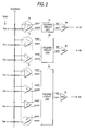
- FIG. 1 is a diagram showing functional blocks of a folding/interpolation A/D converter according to an embodiment of the present invention
- FIG. 2 is a detailed block diagram showing a folding architecture according to the embodiment of the present invention.
- FIG. 3 is a detailed block diagram showing a folding/interpolation architecture according to the embodiment of the present invention.
- FIGS. 4A and 4B are conceptual graphs for explaining the relationship between differential analog input signals Vinp/Vinm and differential reference voltages Vrefp/Vrefm according to the embodiment of the present invention.
- FIG. 5 is a chart showing reference voltages Vrefp of respective circuits
- FIG. 6 is a waveform chart for explaining the operation of the A/D converter according to the embodiment of the present invention.
- FIG. 7 is a waveform chart for explaining the operation of the A/D converter according to the embodiment of the present invention.
- FIGS. 8A and 8B are diagrams showing the circuitry and the input/output property of pre-amplifiers 1 a to 1 h respectively;
- FIGS. 9A and 9B are graphs showing a variation of a transconductance gm in accordance with how to take a reference voltage in a pre-amplifier respectively;
- FIG. 10 is a circuit diagram showing a folding circuit 2 a for G 7 ;
- FIGS. 11A to 11 D are operating waveform charts of the folding circuit 2 a for G 7 respectively;
- FIG. 12 is a circuit diagram showing a folding circuit 2 b for G 6 ;
- FIGS. 13A to 13 D are operating waveform charts of the folding circuit 2 b for G 6 respectively;
- FIG. 14 is a circuit diagram showing a folding circuit 2 c for G 5 .
- FIGS. 15A to 15 D are operating waveform charts of the folding circuit 2 c for G 5 respectively;
- FIGS. 16A and 16B are diagrams showing the circuitry and the input/output property of a sine wave generator
- FIG. 17 is a operating waveform chart of a current interpolation circuit.
- FIG. 18 is a waveform chart showing an example of interpolation based on the current interpolation circuit.
- FIG. 1 is a functional block diagram of a folding-interpolation A/D converter according to the embodiment.
- This A/D converter has 8-bit resolution, but, in the A/D converter, different architectures are adopted between a circuit for generating higher 3 bits of digital data and a circuit for generating lower 5 bits of digital data.
- the circuit for generating higher 3 bits has a folding architecture.
- the circuit for generating lower 5 bits has an architecture in which folding and interpolation are combined.
- the folding architecture is constituted by pre-amplifiers 1 a to 1 c for amplifying potential differences between differential analog input signals (Vinp/Vinm) and differential reference voltages (Vrefp/Vrefn), 3 folding circuits 2 a to 2 c for outputting differential current pairs folded by receiving the outputs of the pre-amplifiers 1 a to 1 c, and three comparators 3 a to 3 c for comparing the differential current pairs and outputting higher 3 bits of a Gray code.
- the comparators 3 a to 3 c are current comparators.
- the folding/interpolation architecture corresponding to lower 5 bits is constituted by pre-amplifiers 1 d to 1 g, sine wave generators 4 a to 4 d for outputting 4-phase sine wave pairs the phases of which are shifted by 45° sequentially in accordance with the outputs of the pre-amplifiers 1 d to 1 g, a current interpolation circuit 5 for interpolating the 4-phase sine wave pairs and outputting 32 sine wave pairs the phases of which are shifted by 5.625° sequentially, 32 comparators 6 for comparing the sine wave pairs and outputting binary data, and a Gray code encoder 7 for encoding the binary data into an n-bit Gray code.
- the present invention is not limited thereto, but may be designed so that, for example, two-phase sine wave pairs the phases of which are shifted by 90° sequentially are generated and interpolated. In this case, it will go well if two sine wave generators are provided.
- the architecture has an analog preprocessing circuit in the left side and a digital circuit in the right side with respect to the comparators 3 a to 3 c and 6 which are aligned, as the boundary near the center of FIG. 1 .
- the analog preprocessing circuit is the general term for the pre-amplifiers 1 a to 1 g, the folding circuits 2 a to 2 c, the sine wave generators 4 a to 4 d, and the current interpolation circuit 5 .
- An analog signal which is a target for A/D conversion is supplied as differential analog input signals (Vinp/Vinm).
- the differential reference voltages (Vrefp/Vrefm) are generated from connection nodes of 72 resistor strings 8 .
- the differential analog input signals (Vinp/Vinm) are analog-encoded by the above-mentioned analog preprocessing circuit, and thereafter digitized by the comparators 3 a to 3 c and 6 .
- the outputs of the comparators 3 a to 3 c are used directly as higher 3 bits (G 7 , G 6 and G 5 ) of a Gray code.
- Lower 5 bits are encoded into Gray code bits (G 4 to G 0 ) by the Gray code encoder 7 .
- the eight bits (G 7 to G 0 ) of the Gray code are outputted through DFFs 9 a to 9 d at a fixed timing.
- an overflow/underflow detection bit (OU)
- an error correction bit (ERRC)
- a circuit for overflow/underflow detection has a configuration similar to the folding architecture for the higher 3 bits. That is, the circuit is constituted by a pre-amplifier 1 h, a folding circuit 2 d and a comparator 3 d.
- the differential analog input signals (Vinp/Vinm) are sampled and held by a track hold circuit 10 , and thereafter applied to the pre-amplifiers 1 a to 1 g.
- the track hold circuit 10 samples the differential analog input signals (Vinp/Vinm), for example, in every period when a clock signal clk is in an H-level.
- the track hold circuit 10 holds and outputs the levels of the signals during the period.
- the clock signal clk is supplied to the comparators 3 a to 3 d and 6 and the DFFs 9 a to 9 e in common so as to synchronize the operations of those circuits, That is, the comparators 3 a to 3 d perform a comparison operation in the period when the clock signal clk is in the H-level. Consequently, an A/D conversion error due to signal delay is prevented from occurring, so that the A/D conversion accuracy can be improved.
- FIG. 2 is a detailed block diagram showing a folding architecture for generating higher 3 bits.
- FIG. 3 is a detailed block diagram showing a folding/interpolation architecture for generating lower 5 bits.
- the pre-amplifiers 1 a, 1 b and 1 c are supplied not only with differential analog input signals Vinp/Vinm in common but also with different differential reference voltages Vrefp/Vrefm generated from the resistor strings 8 .
- the pre-amplifiers 1 a, 1 b and 1 c include one, two and four differential amplifiers, respectively.
- the pre-amplifiers 1 a, 1 b and 1 c output differential voltage pairs ⁇ srcp 1 , srcm 1 > to ⁇ srcp 4 , srcm 4 >. These differential voltage pairs are supplied to the corresponding folding circuits 2 a to 2 c.
- the folding circuits 2 a to 2 c supply folded differential current pairs ⁇ Iop 7 , Iom 7 >, ⁇ Iop 6 , Iom 6 > and ⁇ Iop 5 , Iom 5 > to the comparators 3 a to 3 c, correspondingly and respectively.
- Vrefp V 36 , V 20 , V 52 , . . .
- the pre-amplifiers 1 d, 1 e, 1 f and 1 g are supplied not only with the differential analog input signals Vinp/Vinm in common but also with different differential reference voltages Vrefp/Vrefm generated from the resistor strings 8 .
- Each of the pre-amplifiers 1 d to 1 g includes nine differential amplifiers.
- Each of the pre-amplifiers 1 d to 1 g outputs amplified differential voltage pairs ⁇ srcp 1 , srcm 1 > to ⁇ srcp 9 , srcm 9 >. These differential voltage pairs are supplied to the corresponding sine wave generators 4 a to 4 d in the next stage. Then, the sine wave generators 4 a to 4 d output 4-phase sine wave pairs ⁇ Sinp 0 , Sinm 0 > to ⁇ Sinp 3 , Sinm 3 >, respectively. These sine wave pairs are interpolated by the current interpolation circuit 5 in the further next stage. Thus, 32-phase sine wave pairs the phases of which are shifted by 5.625° sequentially are generated. Then, the sine wave pairs are binarized by the 32 comparators 6 , and thereafter Gray-coded (into G 4 to G 0 ) by the Gray code encoder 7 .
- FIGS. 4A and 4B are schematic graphs for explaining the relationship between the differential analog input signals Vinp/Vinm and the differential reference voltages Vrefp/Vrefm in the above-mentioned configuration of the A/D converter.
- FIG. 4A it is desired that the distance between a high voltage Vh and a low voltage Vl is divided equally by the resistor strings, and the reference voltages Vrefp and Vrefm are located in point shaving the same voltage difference from an intermediate voltage (Vh+Vl)/2 (which is a common voltage of the input signal) between the voltages Vh and Vl.
- Vh+Vl intermediate voltage
- FIG. 5 is a chart showing the reference voltages Vrefp for the respective circuits in the above-mentioned configuration.
- the reference numerals in the drawing represent voltages corresponding to the respective numbers of the connection nodes of the resistor strings.
- the full scale is a range of from Vp 4 to Vp 68 .
- Vp 4 and lower voltages are called underflow, and Vp 68 and higher voltages are called overflow.
- FIG. 6 only a single input Vinp is shown as an input voltage Vin for the sake of simplification.
- the folding circuits 1 a, 1 b and 1 c output currents Iop 7 , Iop 6 and Iop 5 folded in positions of respective reference voltages as illustrated in the drawing, respectively.
- the sine wave generators 4 a to 4 d output 4-phase sine waves Sinp 0 to Sinp 3 in accordance with the input voltage Vin. (Minus-side sine waves Sinm 0 to Sinm 3 are not shown.) Then, the current interpolation circuit 5 outputs 32 sine waves obtained by dividing each of the 4-phase sine waves Sinp 0 to Sinp 3 into 8 sine waves. In FIG. 6, an example of interpolation between the sine waves Sinp 0 and Sinp 1 is illustrated.
- cycle codes V 0 to V 31 are obtained as shown in FIG. 7 .
- the cycle codes V 0 to V 31 are encoded by the Gray code encoder 7 .
- lower 5 bits (G 4 to G 0 ) of the Gray code are obtained as illustrated in the drawing.
- FIGS. 8A and 8B are diagrams showing the circuitry and input/output properties of each of the pre-amplifiers 1 a to 1 h.
- the differential analog input signals Vinp/Vinm are paired with the differential reference voltages Vrefp/Vrefm and supplied to the gates of differential MOS transistor pairs (M 11 , M 12 ) and (M 13 , M 14 ) respectively.
- the differential MOS transistor pairs (M 11 , M 12 ) and (M 13 , M 14 ) output a differential voltage pair ⁇ scrp, scrm>.
- the differential voltage pair ⁇ scrp, scrm> are-supplied to each of the folding circuits 2 a to 2 d and the sine wave generators 4 a to 4 d in the next stage.
- FIG. 8B is a graph showing the input/output properties of the circuit shown in FIG. 8 A. The position where the differential voltage pair ⁇ scrp, scrm> cross each other can be changed by changing the differential reference voltages Vrefp/Vrefm.
- the reference voltages Vrefp/Vrefm are set to take values satisfying the following Expression 1, as has been already described above.
- FIGS. 9A and 9B are charts showing a variation of a transconductance gm in accordance with the way to take a reference voltage in the pre-amplifiers respectively.
- FIG. 9A shows the case that Expression 1 is satisfied
- FIG. 9B shows the case that Expression 1 is not satisfied.
- the value of the transconductance gm in the case where Expression 1 is not satisfied becomes smaller than that in the case that Expression 1 is satisfied.
- the folding circuits 2 a, 2 b and 2 c are analog encoders for generating higher 3 bits (G 7 , G 6 and G 5 ). There are used three kinds of folding circuits, that is, the folding circuit 2 a for G 7 , the folding circuit 2 b for G 6 and the folding circuit 2 c for G 5 .
- FIG. 10 is a circuit diagram showing the folding circuit 2 a for G 7 .
- This circuit is constituted by three blocks of a PMOS current mirror circuit (M 1 ), a PMOS buffer (M 2 ) and an NMOS differential transistor pair (M 3 ).
- the current mirror circuit (M 1 ) supplies a current Ib to lines vddp and vddm which are current channels.
- a differential voltage pair ⁇ scrp 1 , scrm 1 > outputted from the pre-amplifier 1 a are applied to the differential transistor pair (M 3 ).
- a current source Ia is connected to the differential transistor pair (M 3 ).
- the currents Im and Ip flowing in the differential transistor pair (M 3 ) are extracted from the currents in the lines vddp and vddm so that a differential current pair ⁇ Iop 7 , Iom 7 > are outputted from the ends of the lines vddp and vddm.
- FIGS. 11A to 11 D are operating waveform charts of the folding circuit 2 a. Since the differential transistor pair (M 3 ) are cross-connected to the lines vddp and vddm, the current difference between the currents Ip and Im and the current difference between the currents Iop 7 and Iom 7 are always equal to Ia. As shown in FIG. 11C, the differential current pair ⁇ Iop 7 , Iom 7 > have such an input/output property that the pair ⁇ iop 7 , Iom 7 > are folded in the position of a reference voltage (in the position of the intermediate voltage V 36 in this case).
- the binarized data has an input/output property shown in FIG. 11 D and forms digital data for the most significant bit (G 7 ) as it is.
- the folding circuit 2 a operates in a current mode so that it does not need a large voltage amplitude. Therefore, the folding circuit 2 a is advantageous to a reduced voltage. Likewise, this applies to all of the circuits which will be described below.
- FIG. 12 is a circuit diagram showing the folding circuit 2 b for G 6 .
- This circuit is constituted by three blocks of a current mirror circuit (M 4 ), a PMOS buffer (M 5 ) and NMOS differential transistor pairs (M 6 ).
- Differential voltage pairs ⁇ scrp 1 , scrm 1 >, ⁇ scrp 2 , scrm 2 > and ⁇ Vss, Vdd> are applied to the three differential transistor pairs (M 6 ).
- Vss designates a ground voltage
- Vdd designates a power supply voltage.
- the differential transistor pairs are cross-connected alternately to lines vddp and vddm.
- the differential transistor pair to which the differential voltage pair ⁇ Vss, Vdd> are applied are provided to make a current of not lower than Ia always flow to be one of a current pair ⁇ Ip, Im>. Without such a differential transistor pair, the current pair ⁇ Ip, Im> could not form a differential signal.
- FIGS. 13A to 13 D are operating waveform charts of the folding circuit 2 b. Since the differential transistor pairs are cross-connected, currents in a range of from Ia to 2 Ia flow as the current pair ⁇ Ip, Im>. Then, a differential current pair ⁇ Iop 6 , lom 6 > have such an input/output property that the pair ⁇ Iop 6 , Iom 6 > are folded in the positions of two reference voltages (V 20 and V 52 ). When the differential current pair ⁇ Iop 6 , Iom 6 > are binarized by the comparator 3 b, the binarized data has an input/output property shown in FIG. 13 D and forms digital data for a bit (G 6 ) next to the most significant bit (G 7 ) as it is.
- FIG. 14 is a circuit diagram showing the folding circuit 2 c for G 5 .
- This circuit is constituted by three blocks of a current mirror circuit (M 7 ), a PMOS buffer (M 8 ) and NMOS differential transistor pairs (M 9 ).
- Differential voltage pairs ⁇ scrp 1 , scrm 1 > to ⁇ scrp 4 , scrm 4 > and ⁇ Vss, Vdd> are applied to the five differential transistor pairs (M 9 ).
- FIGS. 15A to 15 D are operating waveform charts of the folding circuit 2 c.
- a differential current pair ⁇ Iop 5 , Ior 5 > have such an input/output property that the pair ⁇ Iop 5 , Iom 5 > are folded in the positions of four reference voltages.
- the binarized data has an input/output property shown in FIG. 15 D and forms digital data for a bit (G 5 ) next to the bit (G 6 ) as it is.
- FIG. 15C it is understood from FIG. 15C that all the maximum output current differences take the value of Ia.
- the maximum current differences can be increased if the value of the current source Ia for the differential transistor pairs is increased.
- the load on the comparator 3 a can be reduced.
- the current Ib becomes a factor to define the speed of the circuit. If the current 1 b is increased, the circuit speed is increased. This applies to the other folding circuits 2 a and 2 b.
- the sine wave generators 4 a to 4 d are analog encoders for generating lower bits.
- FIGS. 16A and 16B are a diagram and a chart showing a sine wave generator.
- the sine wave generator has, basically, a configuration similar to that of a folding circuit. That is, the sine wave generator is constituted by a current mirror circuit (M 10 ) and NMOS differential transistor pairs (M 11 ) Differential voltage pairs ⁇ scrp 1 , scrm 1 > to ⁇ scrp 9 , scrm 9 > are applied to the 9 differential transistor pairs (M 11 ) respectively.
- the 9 differential transistor pairs are cross-connected alternately to lines vddp and vddm which are current channels.
- a sine wave current pair ⁇ Isinp, Isinm> are outputted from the ends of the lines vddp and vddm.
- FIG. 16B is an operating waveform chart showing the input/output property (of Isin relative to Vin), having a zero-crossing point in the position of each reference voltage. Because the waveform looks like a sine wave due to such a property, the circuit is referred to as a sine wave generator. In the same manner, 4-phase sine wave pairs ⁇ Isinp 0 , Isinm 0 > to ⁇ Isinp 3 , Isinm 3 > the phases of which are shifted by 45° sequentially can be generated by four circuits which are similar to one another but have different reference voltages.
- the current interpolation circuit is a circuit for interpolating the above-mentioned 4-phase sine waves with a current so as to generate 32-phase sine wave current pairs.
- FIG. 17 is a circuit diagram of the current interpolation circuit.
- the two sine waves Isinp 0 and Isinp 1 outputted from the sine wave generators and shifted in phase by 45° sequentially are supplied as input currents 36 Ia and 36 Ib in FIG. 17 . That is, it is characteristic that the outputs of the sine wave generators are connected directly to the inputs of the current interpolation circuit.
- any interface such as a buffer circuit is omitted in this configuration.
- the input currents 36 Ia and 36 Ib are supplied to the sources of two parallel-connected MOS transistor groups M 12 and M 13 respectively. Numbers written in the vicinity of the respective MOS transistors designate relative magnitudes of gate widths of the transistors. Therefore, the input currents 36 Ia and 36 Ib are divided in accordance with the ratios of the gate widths of the MOS transistors respectively. That is, the input current 36 Ia is divided into eight stages 1 Ia to 8 Ia, and the input current 36 Ib is divided into eight stages 1 Ib to 8 Ib. Because the gate widths of the MOS transistors can be machined with a high accuracy by a MOS process, there is an advantage that the current division ratios can be determined with precision.
- FIG. 18 is a waveform graph showing an example of such interpolation.
- the ratio of the gate widths of the respective MOS transistors is set to be 1:2:3:4:5:6:7:8 in the above-mentioned interpolation example, another ratio different from the above ratio may be set in consideration to the nonlinear property of sine waves.
- the sine wave pairs generated thus are binarized by the comparators 6 , and further encoded by the Gray code encoder. Thus, lower 5 bits (G 4 to G 0 ) are generated.
- Each of the comparators 3 a to 3 d and 6 is a circuit for comparing input Currents. If a plus-side input current is larger than a minus-side input current, the comparator outputs a digital signal 1 . On the other hand, if the plus-side input current is smaller than the minus-side input current, the comparator outputs a digital signal 0 . Since a known circuitry maybe used, its description is omitted here.
- the Gray code encoder is a circuit for encoding the 32-phase outputs from the current interpolation circuit into a Gray code by use of Exclusive OR circuits which will be described later. That is, the following operations are given to the cycle code outputs V 0 to V 31 of the comparators shown in FIG. 7 so as to convert the outputs V 0 to V 31 into a Gray code.
- G 1 V 2 *V 6 *V 10 *V 14 *V 18 *V 22 *V 26 *V 30
- the present invention has main effects as follows.
- the total circuit quantity and the total power consumption can be reduced on a large scale while keeping a speed equal to that in a conventional parallel-connected A/D converter.
- a conventional parallel-connected A/D converter For example, in the case of 8-bit resolution, about 40 comparators are required (while 256 comparators are required in the parallel-connected type).
- a digital encoder is reduced in size on a large scale. As a result, both the circuit quantity and the power consumption of the A/D converter according to the present invention as a whole are reduced to about 1 ⁇ 4 in comparison with the conventional parallel-connected A/D converter.
- CMOS analog preprocessing circuits folding circuits, sine wave generators, and a current interpolation circuit
- a low voltage operation can be carried out.
- the A/D converter according to the present invention can be provided by an integrated circuit of fine CMOS transistors. According to circuit simulation, it was proved that the A/D converter according to the present invention could be operated with power supply voltage of 3V.
- the sine wave generators and the current interpolation circuit are constituted by CMOS while the outputs of the sine wave generators are connected directly to the inputs of the current interpolation circuit. Accordingly, the circuitry is simplified while a high-speed operation can be carried out.
Abstract
Description
Claims (11)
Applications Claiming Priority (3)
| Application Number | Priority Date | Filing Date | Title |
|---|---|---|---|
| JPP.2000-012706 | 2000-01-21 | ||
| JP2000012706A JP3520233B2 (en) | 2000-01-21 | 2000-01-21 | AD conversion circuit |
| JP2000-012706 | 2000-01-21 |
Publications (2)
| Publication Number | Publication Date |
|---|---|
| US20010040522A1 US20010040522A1 (en) | 2001-11-15 |
| US6480133B2 true US6480133B2 (en) | 2002-11-12 |
Family
ID=18540394
Family Applications (1)
| Application Number | Title | Priority Date | Filing Date |
|---|---|---|---|
| US09/766,257 Expired - Fee Related US6480133B2 (en) | 2000-01-21 | 2001-01-19 | Low-power analog-to-digital converter |
Country Status (5)
| Country | Link |
|---|---|
| US (1) | US6480133B2 (en) |
| JP (1) | JP3520233B2 (en) |
| KR (1) | KR100366520B1 (en) |
| CN (1) | CN1308412B (en) |
| TW (1) | TW472459B (en) |
Cited By (8)
| Publication number | Priority date | Publication date | Assignee | Title |
|---|---|---|---|---|
| US20030076253A1 (en) * | 2001-10-03 | 2003-04-24 | Roovers Raf Lodewijk Jan | Analogue to digital converter |
| US20030143795A1 (en) * | 2001-12-17 | 2003-07-31 | Weidong Guo | Current steering folding circuit |
| US20050168368A1 (en) * | 2004-01-29 | 2005-08-04 | Kawasaki Microelectronics, Inc. | Error correction circuit and A/D converter |
| US20060055578A1 (en) * | 2004-08-18 | 2006-03-16 | Matsushita Electric Industrial Co., Ltd. | A/D converter and A/D converting system |
| US20080300808A1 (en) * | 2005-10-14 | 2008-12-04 | Hexagon Metrology Ab | Method for Signal Processing of Capacitive Measurement Scales |
| US20110001648A1 (en) * | 2006-09-04 | 2011-01-06 | Takeshi Ohkawa | Folding circuit and analog-to-digital converter |
| US8344795B2 (en) | 2011-01-20 | 2013-01-01 | International Business Machines Corporation | Self-calibrated, broadband, tunable, active filter with unity gain cells for multi-standard and/or multiband channel selection |
| US8350738B2 (en) | 2011-01-20 | 2013-01-08 | International Business Machines Corporation | Track and hold amplifiers and digital calibration for analog-to-digital converters |
Families Citing this family (10)
| Publication number | Priority date | Publication date | Assignee | Title |
|---|---|---|---|---|
| CN100530974C (en) * | 2004-02-25 | 2009-08-19 | 三菱电机株式会社 | Waveform generation method, radar device, and oscillator for radar device |
| CN101076053B (en) * | 2007-06-21 | 2010-10-06 | 吴壬华 | Method and circuit for multi-channel photoelectric isolated voltage |
| US7567197B2 (en) * | 2007-09-17 | 2009-07-28 | Samsung Electronics Co., Ltd. | Cascade comparator and control method thereof |
| FR2929777B1 (en) | 2008-04-04 | 2010-04-23 | E2V Semiconductors | FAST ANALOGUE-DIGITAL CONVERTER HAVING AN IMPROVED SIGNAL FOLDING STRUCTURE BY REDUCING THE NUMBER OF ELEMENTARY CELLS |
| CN101676690B (en) * | 2008-09-19 | 2011-11-30 | 鸿富锦精密工业(深圳)有限公司 | Driving device |
| EP2485400B1 (en) * | 2009-01-26 | 2014-06-25 | Fujitsu Semiconductor Limited | Sampling |
| KR101291803B1 (en) | 2010-01-28 | 2013-07-31 | 엘지디스플레이 주식회사 | Folding Analog Digital Converter |
| US8502718B2 (en) * | 2010-11-19 | 2013-08-06 | Fortemedia, Inc. | Analog-to-digital converter and analog-to-digital conversion method |
| US8670572B2 (en) * | 2010-11-19 | 2014-03-11 | Fortemedia, Inc. | Analog-to-digital converter and analog-to-digital conversion method |
| US8670853B2 (en) * | 2010-11-19 | 2014-03-11 | Fortemedia, Inc. | Analog-to-digital converter, sound processing device, and analog-to-digital conversion method |
Citations (4)
| Publication number | Priority date | Publication date | Assignee | Title |
|---|---|---|---|---|
| US5309157A (en) * | 1992-11-06 | 1994-05-03 | National Semiconductor Corporation | Analog to digital converter using folder reference circuits |
| JPH08149006A (en) | 1994-11-24 | 1996-06-07 | Tera Tec:Kk | Analog-digital converter |
| US6175323B1 (en) * | 1997-08-15 | 2001-01-16 | Texas Instruments Incorporated | Differential pair-based folding interpolator circuit for an analog-to-digital converter |
| US6239733B1 (en) * | 1999-05-28 | 2001-05-29 | United Microelectronics Corp. | Current interpolation circuit for use in an A/D converter |
-
2000
- 2000-01-21 JP JP2000012706A patent/JP3520233B2/en not_active Expired - Fee Related
-
2001
- 2001-01-15 TW TW090100829A patent/TW472459B/en not_active IP Right Cessation
- 2001-01-19 US US09/766,257 patent/US6480133B2/en not_active Expired - Fee Related
- 2001-01-20 KR KR10-2001-0003381A patent/KR100366520B1/en not_active IP Right Cessation
- 2001-01-21 CN CN011030097A patent/CN1308412B/en not_active Expired - Fee Related
Patent Citations (4)
| Publication number | Priority date | Publication date | Assignee | Title |
|---|---|---|---|---|
| US5309157A (en) * | 1992-11-06 | 1994-05-03 | National Semiconductor Corporation | Analog to digital converter using folder reference circuits |
| JPH08149006A (en) | 1994-11-24 | 1996-06-07 | Tera Tec:Kk | Analog-digital converter |
| US6175323B1 (en) * | 1997-08-15 | 2001-01-16 | Texas Instruments Incorporated | Differential pair-based folding interpolator circuit for an analog-to-digital converter |
| US6239733B1 (en) * | 1999-05-28 | 2001-05-29 | United Microelectronics Corp. | Current interpolation circuit for use in an A/D converter |
Cited By (15)
| Publication number | Priority date | Publication date | Assignee | Title |
|---|---|---|---|---|
| US20030076253A1 (en) * | 2001-10-03 | 2003-04-24 | Roovers Raf Lodewijk Jan | Analogue to digital converter |
| US6731231B2 (en) * | 2001-10-03 | 2004-05-04 | Koninklijke Philips Electronics N.V. | Analogue to digital converter |
| US20030143795A1 (en) * | 2001-12-17 | 2003-07-31 | Weidong Guo | Current steering folding circuit |
| US7009547B2 (en) * | 2001-12-17 | 2006-03-07 | University Of Utah Research Foundation | Current steering folding circuit |
| US20050168368A1 (en) * | 2004-01-29 | 2005-08-04 | Kawasaki Microelectronics, Inc. | Error correction circuit and A/D converter |
| US6985097B2 (en) * | 2004-01-29 | 2006-01-10 | Kawasaki Microelectronics, Inc. | Error correction circuit and A/D converter |
| US20060055578A1 (en) * | 2004-08-18 | 2006-03-16 | Matsushita Electric Industrial Co., Ltd. | A/D converter and A/D converting system |
| US7061419B2 (en) * | 2004-08-18 | 2006-06-13 | Matsushita Electric Industrial Co., Ltd. | A/D converter and A/D converting system |
| US20080300808A1 (en) * | 2005-10-14 | 2008-12-04 | Hexagon Metrology Ab | Method for Signal Processing of Capacitive Measurement Scales |
| US7956622B2 (en) * | 2005-10-14 | 2011-06-07 | Hexagon Metrology Ab | Method for signal processing of capacitive measurement scales |
| US20110001648A1 (en) * | 2006-09-04 | 2011-01-06 | Takeshi Ohkawa | Folding circuit and analog-to-digital converter |
| US7999717B2 (en) * | 2006-09-04 | 2011-08-16 | Sony Corporation | Folding circuit and analog-to-digital converter |
| US8344795B2 (en) | 2011-01-20 | 2013-01-01 | International Business Machines Corporation | Self-calibrated, broadband, tunable, active filter with unity gain cells for multi-standard and/or multiband channel selection |
| US8350738B2 (en) | 2011-01-20 | 2013-01-08 | International Business Machines Corporation | Track and hold amplifiers and digital calibration for analog-to-digital converters |
| US8487693B2 (en) | 2011-01-20 | 2013-07-16 | International Business Machines Corporation | Self calibrated, broadband, tunable, active oscillator with unity gain cells for multi-standard and/or multiband channel selection |
Also Published As
| Publication number | Publication date |
|---|---|
| JP2001203578A (en) | 2001-07-27 |
| KR20010076416A (en) | 2001-08-11 |
| CN1308412A (en) | 2001-08-15 |
| CN1308412B (en) | 2010-05-26 |
| US20010040522A1 (en) | 2001-11-15 |
| TW472459B (en) | 2002-01-11 |
| JP3520233B2 (en) | 2004-04-19 |
| KR100366520B1 (en) | 2003-01-09 |
Similar Documents
| Publication | Publication Date | Title |
|---|---|---|
| US6480133B2 (en) | Low-power analog-to-digital converter | |
| US6121912A (en) | Subranging analog-to-digital converter and method | |
| US5489904A (en) | Analog current mode analog/digital converter | |
| Venes et al. | An 80-MHz, 80-mW, 8-b CMOS folding A/D converter with distributed track-and-hold preprocessing | |
| CN102142840B (en) | Folding analog-to-digital converter | |
| EP0938189A2 (en) | Multistage analog-to-digital converter employing dither | |
| JP4349445B2 (en) | Flash AD converter | |
| US6707413B2 (en) | A/D converter | |
| KR20070076429A (en) | Analog-to-digital conversion circuit | |
| KR100799683B1 (en) | Cascaded folding and interpolating analog-to-digital converter | |
| US6445329B1 (en) | High speed analog to digital converter | |
| JP3555956B2 (en) | Folding stage and folded analog-to-digital converter | |
| US6420983B1 (en) | On-line offset cancellation in flash A/D with interpolating comparator array | |
| US5739781A (en) | Sub-ranging analog-to-digital converter with open-loop differential amplifiers | |
| KR101644999B1 (en) | Low-Power Analog Digital Converter By Using Time-Domain Multi-Stage Interpolation | |
| US6501412B2 (en) | Analog-to-digital converter including a series of quantizers interconnected in cascade | |
| JP3555955B2 (en) | Folding stage for folded analog-to-digital converter | |
| CN100511978C (en) | Transconductance amplifier, analog-to-digital converter and operating method thereof, and current generation method | |
| KR20000027231A (en) | Folding interpolation analog-digital converter of high speed and low electric power | |
| Agrawal et al. | A threshold inverter quantization based folding and interpolation ADC in 0.18 μm CMOS | |
| JP3444580B2 (en) | Interpolation type A / D converter | |
| KR20020022159A (en) | Folding interpolation A/D converter | |
| JP2009296271A (en) | Latch circuit and a/d converter | |
| Mikheev et al. | Formalization of folding and interpolating ADC architecture | |
| US6369742B1 (en) | Selective over-ranging in folding and averaging integrated circuits |
Legal Events
| Date | Code | Title | Description |
|---|---|---|---|
| AS | Assignment |
Owner name: SANYO ELECTRIC CO., LTD., JAPAN Free format text: ASSIGNMENT OF ASSIGNORS INTEREST;ASSIGNORS:KOBAYASHI, HARUO;KIMURA, YASUYUKI;REEL/FRAME:011483/0618 Effective date: 20010112 Owner name: KOBAYASHI, HARUO, JAPAN Free format text: ASSIGNMENT OF ASSIGNORS INTEREST;ASSIGNORS:KOBAYASHI, HARUO;KIMURA, YASUYUKI;REEL/FRAME:011483/0618 Effective date: 20010112 |
|
| FEPP | Fee payment procedure |
Free format text: PAYOR NUMBER ASSIGNED (ORIGINAL EVENT CODE: ASPN); ENTITY STATUS OF PATENT OWNER: LARGE ENTITY |
|
| FPAY | Fee payment |
Year of fee payment: 4 |
|
| FPAY | Fee payment |
Year of fee payment: 8 |
|
| REMI | Maintenance fee reminder mailed | ||
| LAPS | Lapse for failure to pay maintenance fees | ||
| AS | Assignment |
Owner name: SYSTEMS SOLUTIONS CO., LTD., JAPAN Free format text: CHANGE OF NAME;ASSIGNOR:SANYO SEMICONDUCTOR CO., LTD.;REEL/FRAME:034285/0006 Effective date: 20140228 |
|
| STCH | Information on status: patent discontinuation |
Free format text: PATENT EXPIRED DUE TO NONPAYMENT OF MAINTENANCE FEES UNDER 37 CFR 1.362 |
|
| AS | Assignment |
Owner name: SYSTEM SOLUTIONS CO., LTD, JAPAN Free format text: ASSIGNMENT OF ASSIGNORS INTEREST;ASSIGNOR:SANYO ELECTRIC CO., LTD.;REEL/FRAME:034531/0046 Effective date: 20110101 |
|
| FP | Lapsed due to failure to pay maintenance fee |
Effective date: 20141112 |
|
| AS | Assignment |
Owner name: SYSTEM SOLUTIONS CO., LTD., JAPAN Free format text: CORRECTIVE ASSIGNMENT TO CORRECT THE REMOVAL OF APPLICATION NUMBERS THAT WERE INADVERTENTLY ADDED. PREVIOUSLY RECORDED ON REEL 034285 FRAME 0006. ASSIGNOR(S) HEREBY CONFIRMS THE ASSIGNMENT;ASSIGNOR:SANYO SEMICONDUCTOR CO., LTD.;REEL/FRAME:034745/0927 Effective date: 20140228 Owner name: SYSTEM SOLUTIONS CO., LTD., JAPAN Free format text: CORRECTIVE ASSIGNMENT TO CORRECT THE APPLICATION NUMBERS . PREVIOUSLY RECORDED ON REEL 034285 FRAME 0006. ASSIGNOR(S) HEREBY CONFIRMS THE ASSIGNMENT;ASSIGNOR:SANYO SEMICONDUCTOR CO., LTD.;REEL/FRAME:034745/0927 Effective date: 20140228 |