US6476341B2 - Cleaning device with deeply reaching plasma and assisting electrodes - Google Patents

Cleaning device with deeply reaching plasma and assisting electrodes Download PDF

Info

Publication number
US6476341B2
US6476341B2 US09/742,430 US74243000A US6476341B2 US 6476341 B2 US6476341 B2 US 6476341B2 US 74243000 A US74243000 A US 74243000A US 6476341 B2 US6476341 B2 US 6476341B2
Authority
US
United States
Prior art keywords
plasma
cleaning device
supporting racks
deeply reaching
electrodes
Prior art date
Legal status (The legal status is an assumption and is not a legal conclusion. Google has not performed a legal analysis and makes no representation as to the accuracy of the status listed.)
Expired - Fee Related
Application number
US09/742,430
Other versions
US20010020477A1 (en
Inventor
Chia-Yuan Hsu
Yong-Hau Foo
Paul Hong
Current Assignee (The listed assignees may be inaccurate. Google has not performed a legal analysis and makes no representation or warranty as to the accuracy of the list.)
Nano Electronics and Micro System Technologies Inc
Original Assignee
Advanced Plasma and Thin Films Technologies Inc
Priority date (The priority date is an assumption and is not a legal conclusion. Google has not performed a legal analysis and makes no representation as to the accuracy of the date listed.)
Filing date
Publication date
Priority claimed from TW89204026U external-priority patent/TW449227U/en
Application filed by Advanced Plasma and Thin Films Technologies Inc filed Critical Advanced Plasma and Thin Films Technologies Inc
Assigned to ADVANCED PLASMA AND THIN FILMS TECHNOLOGIES, INC. reassignment ADVANCED PLASMA AND THIN FILMS TECHNOLOGIES, INC. ASSIGNMENT OF ASSIGNORS INTEREST (SEE DOCUMENT FOR DETAILS). Assignors: FOO, YONG-HAU, HSU, CHIA-YUAN, HONG, PAUL
Publication of US20010020477A1 publication Critical patent/US20010020477A1/en
Priority to US10/115,067 priority Critical patent/US6603091B2/en
Application granted granted Critical
Publication of US6476341B2 publication Critical patent/US6476341B2/en
Assigned to NANO ELECTRONICS AND MICRO SYSTEM TECHNOLOGIES, INC. reassignment NANO ELECTRONICS AND MICRO SYSTEM TECHNOLOGIES, INC. ASSIGNMENT OF ASSIGNORS INTEREST (SEE DOCUMENT FOR DETAILS). Assignors: ADVANCED PLASMA AND THIN FILMS TECHNOLOGIES, INC.
Anticipated expiration legal-status Critical
Expired - Fee Related legal-status Critical Current

Links

Images

Classifications

    • BPERFORMING OPERATIONS; TRANSPORTING
    • B08CLEANING
    • B08BCLEANING IN GENERAL; PREVENTION OF FOULING IN GENERAL
    • B08B7/00Cleaning by methods not provided for in a single other subclass or a single group in this subclass

Definitions

  • the present invention relates to a cleaning device with deeply reaching plasma and assisting electrodes, and particularly to one which is used in cleaning flat-board shaped things such as silicon wafers, Cu lead frames, etc.
  • the integrated circuits can have dirt unwarily attached to them because of the manufacturing conditions and dust in the environment. Therefore, it is necessary that the dirt and dust are removed from the integrated circuits. Otherwise, other necessary materials cannot be appropriately attached to the integrated circuits.
  • Cleaning devices for integrated circuits can also be used in surface processing, and plating such as plasma ashing of silicon, removing of passivation layer.
  • the cleaning device deeply reaching plasma and assisting electrodes has:
  • the supporting racks receiving flat boards to be cleaned therein; the supporting racks having openings for permitting the flat boards to be inserted;
  • the plasma sources being disposed beside two sides of the supporting racks; the plasma sources being capable of sending out plasma to clean the flat boards;
  • the metallic grids being disposed adjacent to the supporting rocks and the plasma sources; electric voltage being applied to the metallic grids to help the plasma of the plasma sources pushed deeply into the supporting racks for permitting the plasma to clean the flat boards evenly and sufficiently.
  • FIG. 1 is a block diagram of the structure of the cleaning device of the present invention.
  • FIG. 2 is a view of the cleaning device of the pre sent invention with inductively coupling plasma.
  • FIG. 3 is a view of the cleaning device with inductively coupling plasma according to a second embodiment of the present invention.
  • FIG. 4 is an exploded perspective view of the supporting rack of the present invention.
  • FIG. 5 is another supporting rack according to the present invention.
  • FIG. 6 is a block diagram of the structure of the cleaning device without holding members according to the present invention.
  • FIG. 7 is a view of the cleaning device of inductively coupling plasma without holding members.
  • FIG. 8 is a view of the cleaning device with insulating cushions of a first type.
  • FIG. 9 is a view of the cleaning device with insulating cushions of a second type.
  • FIG. 10 is a view of the cleaning device with insulating cushions of a third type.
  • FIG. 11 is a view of the cleaning device with flat-spiral-shaped antennas.
  • FIG. 12 is a perspective view of the cleaning device with hollow cathode discharge of a first type.
  • FIG. 13 is side view of the cleaning device in FIG. 12 .
  • FIG. 14 is a side view of the cleaning device with hollow cathode discharge of a second type.
  • FIG. 15 is a block diagram of the cleaning device with magnetic field and holding member.
  • FIG. 16 is a view of the cleaning device with magnetic field and holding member type one.
  • FIG. 17 is a view of the cleaning device with magnetic field and holding members type two.
  • FIG. 18 is a view of cleaning device with magnetic field and holding members type three.
  • FIG. 19 is a block diagram of the cleaning device with magnetic field, without holding members according to the present invention.
  • FIG. 20 is a view of the cleaning device with magnetic field, without holding members, type one.
  • FIG. 21 is a view of the cleaning device with magnetic field, without holding members, type two.
  • FIG. 22 is an exploded perspective view of the supporting racks of the cleaning device according to a third embodiment of the present invention.
  • FIG. 23 is a perspective view of the supporting rack in FIG. 22 .
  • FIG. 24 is a cross-sectional view of the supporting rack in FIG. 22 .
  • the cleaning device with deeply reaching plasma and assisting electrodes of the present invention includes:
  • the racks 1 each has openings 12 on a front side and a rear side and support protrusions 11 .
  • the racks 1 are further provided with covers 13 having through holes 131 .
  • the covers 13 are fitted to the front and the rear sides of the racks 1 .
  • the racks 1 can also be used without the covers 13 fitted to them.
  • the racks 1 are each provided with elongated holes 14 on two lateral sides.
  • the racks 1 can also be provided without elongated holes 14 on two lateral sides.
  • the openings 12 , the through holes 131 and the elongated holes 14 can help plasma sent into the racks easily;
  • the holding member 2 can be made of insulated materials and conductive materials as well; the holding member 2 can hold the supporting racks 1 ; the cleaning device also can be used without the holding member 2 provided in it; when the holding member 2 is not used, the supporting racks 1 are piled up as shown in FIGS. 6, 7 and 8 ; there can be more than one holding members 2 ;
  • the chamber 3 has a room in it; the supporting racks 1 and the holding members 2 are received in the chamber; the chamber 3 can become vacuum by using a vacuum machine;
  • the plasma source 4 is disposed on two sides of the supporting racks 1 and the holding member 2 ;
  • the plasma source 4 can be ICP (inductively-coupling plasma), HCD (hollow cathode discharge), Helicon or CCP (capacivity-coupling plasma); there can be more than one plasma sources 4 ;
  • the metallic grid 5 is disposed between the supporting racks 1 and the plasma sources 4 ; when electric voltage is applied to the metallic grid 5 , electrons or ions of the plasma are sent into the supporting racks 1 ; thus, the plasma can reach deeply and have desirable cleaning capabilities;
  • the meshes of the metallic grid 5 can be rectangular, round, oval, or honeycomb-shaped, and is about one to twenty millimeters wide, the metallic grid can be formed by various designs such as it is formed apart by plurality horizontal parallel wires, vertical parallel wires, horizontal oblique wires, and vertical oblique wires.
  • the metallic grid 5 can be replaced with metallic plates having through holes on them, the electric voltage applied to the metallic grid 5 can be DCV, unipolar positive or unipolar negative pulse, bipolar pulse or intermediate frequency (40k-13.56 MHz).
  • the things to be cleaned are inserted into the supporting racks 1 and the supporting racks 1 are disposed in the holding member 2 ; then, the holding member 2 is disposed in the chamber 3 , and the metallic grids 5 and the plasma sources 4 are disposed on two sides of the holding member 2 ; in using the cleaning device having no holding member 2 .
  • FIGS. 1, 2 and 3 the things to be cleaned are inserted into the supporting racks 1 and the supporting racks 1 are disposed in the holding member 2 ; then, the holding member 2 is disposed in the chamber 3 , and the metallic grids 5 and the plasma sources 4 are disposed on two sides of the holding member 2 ; in using the cleaning device having no holding member 2 .
  • the things to be cleaned are inserted into the supporting racks 1 , and the racks 1 are disposed in the chamber 3 ; then the plasma sources 4 and the metallic grids 5 are disposed on two sides of the supporting racks 1 ; then, the plasma sources 4 send out plasma, and the bias voltage is applied to the metallic grid 5 . Because the holding members 2 are disposed adjacent to the plasma sources 4 , the things to be cleaned can be sufficiently contacted by the plasma. And, the plasma can flow evenly between the flat-board shaped things to be cleaned.
  • the metallic grid 5 Because of the electric voltage, the metallic grid 5 has either positive electric field of negative electric field; the positive electric field can push the ions of the plasma into the supporting racks 1 , while the negative electric field pushes the electrons of the plasma into the racks 1 . That is, the metallic grid 5 , having electric voltage, can increase the density of the plasma, and push the ions or the electrons of the plasma into the racks 1 deeply. Thus, the cleaning effectiveness and the evenness of the plasma are obviously increased.
  • the holding members 2 and the supporting racks 1 are made of conductive materials or not.
  • the supporting racks 1 or the holding members 2 are conductive, we can apply positive or negative bias voltage pulse of low frequency (about 0.1-500 KHZ) to attract electrons or ions for spreading the plasma. And, the action strength of the ions can be controlled to achieve optimum cleaning effect.
  • the racks 1 and the holding members 2 should be in floating potential type for preventing the bias voltage from being applied on the chamber 3 .
  • the holding members 2 should be insulated; and, referring to FIG.
  • the supporting racks 1 are conductive, the racks 1 are piled up or arrayed with a insulating cushion 21 inserted between the lowest one of the racks 1 and the chamber 3 in order to form a floating potential;
  • the voltage applied to the supporting racks 1 can be positive or negative direct current voltage, pulse voltage (about 0.1-500 KHZ), or intermediate frequency alternating current voltage.
  • the supporting racks 1 or the holding members 2 have antennas 41 disposed on two opposing sides; the antennas 41 can be spiral-shaped, wound up with level-spiral-shaped or flat-spiral-shaped. No matter what kind of shape the antennas 41 have, high frequency power (about 10k-54.24 MHZ) can be sent through the antennas 41 .
  • the antennas 41 can be grounded but they do necessarily have to be grounded. When the antennas 41 are grounded, the potential difference can be reduced, and so the action strength of the ions of the plasma is reduced. When the antennas 41 are not grounded, the potential difference is increased, and so the action strength of the ions is increased. Thus, the action strength of the plasma ions is controlled to achieve optimum cleaning effect.
  • the antennas 41 of the inductively-coupling plasma source are flat-spiral-shaped, and are not grounded, the metallic grid 5 is not a must; the flat-spiral-shaped antennas 41 have negative potential, and therefore have the function of a metallic grid.
  • hollow negative electrodes 42 are disposed on two sides of the holding members 2 ; the hollow negative electrodes 42 have through holes 421 .
  • negative voltage is applied to the hollow negative electrodes 42 , and air is passed through the through holes 421 from outside, negative plasma will be produced on inner sides of the hollow negative electrodes 42 ; the plasma will flow into the supporting racks 1 to clean the plate-shaped things in the racks 1 .
  • the metallic grid 5 is not a must.
  • the hollow negative electrodes 42 having through holes have high voltage, and so have the function of the metallic grid 5 .
  • the cleaning device can be adjusted in a greater range in respect of its cleaning effect.
  • a magnetic field is provided on outside of the plasma source 4 ; namely, magnets 6 are disposed on outside of the plasma sources 4 .
  • the magnets 6 can be electromagnets or permanent magnets so as to provide axial direction or diametric direction of the magnetic field in respect of the plasma sources 4 .
  • buffer members 15 are provided; the buffer members 15 each has a rack part 151 , several buffer plates 152 , an inner frame 153 and an outer fame 154 .
  • the rack parts 151 each has elongated trenches 1514 on outer sides, and support protrusions 1511 corresponding to the support protrusions 11 of the supporting racks 1 .
  • the buffer plates 152 are each located on corresponding ones of the support protrusions 1511 .
  • the outer frame 154 has connecting protrusions 1541 , which engage the elongated trenches 1514 of the rack part 151 when the frame 154 is connected to the rack part 151 with screws.
  • the inner frame 153 also has connecting protrusions 1531 , which engage elongated trenches (not numbered) of the support rack 1 when the frame 153 is connected to the support racks 1 with screws.
  • the buffer plates 152 are protected from falling off the rack part 151 by the frames 153 , 154 .
  • the buffer members 15 are connected to the support racks 1 when the support racks 1 don't have the covers 13 fitted to them.
  • the buffer members 15 can help the plasma spread on the flat-board-shaped things to be cleaned in the support racks 1 evenly, preventing the outer portions of the things to be cleaned from being cleaned too much, and the intermediate portions from being insufficiently cleaned.
  • the buffer plates 15 can be made of metals, waste circuit boards or insulating plates such as Teflon.
  • the things to be cleaned are located on the supporting protrusions 11 of the support racks 1 , and the buffer members 15 are fitted to the support racks as above said, and as shown in FIG. 23 .
  • the buffer plates 152 are each located at a same height as the corresponding things to be cleaned. Then, the support racks 1 are disposed in the cleaning device for the cleaning process.
  • the cleaning device of the present invention can be known to have desirable features as follows.

Abstract

A cleaning device with deeply reaching plasma and assisting electrodes has supporting racks, a chamber, a plasma sources, metallic grids. Flat boards to be cleaned such as circuit boards are located in the supporting racks. The supporting racks are disposed in the chamber. The metallic grids are disposed on two sides of the chamber. The plasma source is disposed next to the metallic grids. Electric voltage is applied to the metallic grids such that plasma from the plasma source can be pushed deeply into the supporting racks to evenly and sufficiently clean the circuit boards.

Description

BACKGROUND OF THE INVENTION
The present invention relates to a cleaning device with deeply reaching plasma and assisting electrodes, and particularly to one which is used in cleaning flat-board shaped things such as silicon wafers, Cu lead frames, etc.
In the process of making integrated circuits, the integrated circuits can have dirt unwarily attached to them because of the manufacturing conditions and dust in the environment. Therefore, it is necessary that the dirt and dust are removed from the integrated circuits. Otherwise, other necessary materials cannot be appropriately attached to the integrated circuits.
Cleaning devices for integrated circuits can also be used in surface processing, and plating such as plasma ashing of silicon, removing of passivation layer.
However, the inventor of the present invention found that conventional cleaning devices with plasma could not clean the circuits very sufficiently because the plasma could not reach deeply enough.
SUMMARY OF THE INVENTION
Therefore, it is a main object of the present invention to provide a cleaning device with deeply reaching plasma and assisting electrodes such that the circuits can be sufficiently cleaned.
The cleaning device deeply reaching plasma and assisting electrodes has:
several supporting racks; the supporting racks receiving flat boards to be cleaned therein; the supporting racks having openings for permitting the flat boards to be inserted;
a chamber; the chamber receiving the supporting racks therein;
several plasma sources; the plasma sources being disposed beside two sides of the supporting racks; the plasma sources being capable of sending out plasma to clean the flat boards;
several metallic grids; the metallic grids being disposed adjacent to the supporting rocks and the plasma sources; electric voltage being applied to the metallic grids to help the plasma of the plasma sources pushed deeply into the supporting racks for permitting the plasma to clean the flat boards evenly and sufficiently.
BRIEF DESCRIPTION OF THE DRAWINGS
This invention will be better understood by referring to the accompanying drawings, wherein:
FIG. 1 is a block diagram of the structure of the cleaning device of the present invention.
FIG. 2 is a view of the cleaning device of the pre sent invention with inductively coupling plasma.
FIG. 3 is a view of the cleaning device with inductively coupling plasma according to a second embodiment of the present invention.
FIG. 4 is an exploded perspective view of the supporting rack of the present invention.
FIG. 5 is another supporting rack according to the present invention.
FIG. 6 is a block diagram of the structure of the cleaning device without holding members according to the present invention.
FIG. 7 is a view of the cleaning device of inductively coupling plasma without holding members.
FIG. 8 is a view of the cleaning device with insulating cushions of a first type.
FIG. 9 is a view of the cleaning device with insulating cushions of a second type.
FIG. 10 is a view of the cleaning device with insulating cushions of a third type.
FIG. 11 is a view of the cleaning device with flat-spiral-shaped antennas.
FIG. 12 is a perspective view of the cleaning device with hollow cathode discharge of a first type.
FIG. 13 is side view of the cleaning device in FIG. 12.
FIG. 14 is a side view of the cleaning device with hollow cathode discharge of a second type.
FIG. 15 is a block diagram of the cleaning device with magnetic field and holding member.
FIG. 16 is a view of the cleaning device with magnetic field and holding member type one.
FIG. 17 is a view of the cleaning device with magnetic field and holding members type two.
FIG. 18 is a view of cleaning device with magnetic field and holding members type three.
FIG. 19 is a block diagram of the cleaning device with magnetic field, without holding members according to the present invention.
FIG. 20 is a view of the cleaning device with magnetic field, without holding members, type one.
FIG. 21 is a view of the cleaning device with magnetic field, without holding members, type two.
FIG. 22 is an exploded perspective view of the supporting racks of the cleaning device according to a third embodiment of the present invention.
FIG. 23 is a perspective view of the supporting rack in FIG. 22.
FIG. 24 is a cross-sectional view of the supporting rack in FIG. 22.
DESCRIPTION OF THE PREFERRED EMBODIMENTS
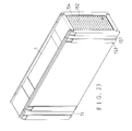
Referring to FIGS. 1, 2 and 3, the cleaning device with deeply reaching plasma and assisting electrodes of the present invention includes:
several supporting racks 1; referring to FIGS. 4 and 5, the racks 1 each has openings 12 on a front side and a rear side and support protrusions 11. Thus, flat boards, and held in position by the support protrusions 11. The racks 1 are further provided with covers 13 having through holes 131. The covers 13 are fitted to the front and the rear sides of the racks 1. The racks 1 can also be used without the covers 13 fitted to them. The racks 1 are each provided with elongated holes 14 on two lateral sides. The racks 1 can also be provided without elongated holes 14 on two lateral sides. The openings 12, the through holes 131 and the elongated holes 14 can help plasma sent into the racks easily;
a holding member 2; the holding member 2 can be made of insulated materials and conductive materials as well; the holding member 2 can hold the supporting racks 1; the cleaning device also can be used without the holding member 2 provided in it; when the holding member 2 is not used, the supporting racks 1 are piled up as shown in FIGS. 6, 7 and 8; there can be more than one holding members 2;
a chamber 3; the chamber 3 has a room in it; the supporting racks 1 and the holding members 2 are received in the chamber; the chamber 3 can become vacuum by using a vacuum machine;
a plasma source 4; the plasma source 4 is disposed on two sides of the supporting racks 1 and the holding member 2; the plasma source 4 can be ICP (inductively-coupling plasma), HCD (hollow cathode discharge), Helicon or CCP (capacivity-coupling plasma); there can be more than one plasma sources 4;
a metallic grid 5; the metallic grid 5 is disposed between the supporting racks 1 and the plasma sources 4; when electric voltage is applied to the metallic grid 5, electrons or ions of the plasma are sent into the supporting racks 1; thus, the plasma can reach deeply and have desirable cleaning capabilities; the meshes of the metallic grid 5 can be rectangular, round, oval, or honeycomb-shaped, and is about one to twenty millimeters wide, the metallic grid can be formed by various designs such as it is formed apart by plurality horizontal parallel wires, vertical parallel wires, horizontal oblique wires, and vertical oblique wires. The metallic grid 5 can be replaced with metallic plates having through holes on them, the electric voltage applied to the metallic grid 5 can be DCV, unipolar positive or unipolar negative pulse, bipolar pulse or intermediate frequency (40k-13.56 MHz).
In using the cleaning device with deeply reaching plasma wherein the holding member 2 is used; referring to FIGS. 1, 2 and 3, the things to be cleaned are inserted into the supporting racks 1 and the supporting racks 1 are disposed in the holding member 2; then, the holding member 2 is disposed in the chamber 3, and the metallic grids 5 and the plasma sources 4 are disposed on two sides of the holding member 2; in using the cleaning device having no holding member 2. Referring to FIGS. 6, 7 and 8, the things to be cleaned are inserted into the supporting racks 1, and the racks 1 are disposed in the chamber 3; then the plasma sources 4 and the metallic grids 5 are disposed on two sides of the supporting racks 1; then, the plasma sources 4 send out plasma, and the bias voltage is applied to the metallic grid 5. Because the holding members 2 are disposed adjacent to the plasma sources 4, the things to be cleaned can be sufficiently contacted by the plasma. And, the plasma can flow evenly between the flat-board shaped things to be cleaned. Because of the electric voltage, the metallic grid 5 has either positive electric field of negative electric field; the positive electric field can push the ions of the plasma into the supporting racks 1, while the negative electric field pushes the electrons of the plasma into the racks 1. That is, the metallic grid 5, having electric voltage, can increase the density of the plasma, and push the ions or the electrons of the plasma into the racks 1 deeply. Thus, the cleaning effectiveness and the evenness of the plasma are obviously increased.
In using the cleaning device with the holding members 2, it doesn't matter whether the holding members 2 and the supporting racks 1 are made of conductive materials or not. When the supporting racks 1 or the holding members 2 are conductive, we can apply positive or negative bias voltage pulse of low frequency (about 0.1-500 KHZ) to attract electrons or ions for spreading the plasma. And, the action strength of the ions can be controlled to achieve optimum cleaning effect. Furthermore, when applying electric voltage to the supporting racks 1 or the holding members 2, the racks 1 and the holding members 2 should be in floating potential type for preventing the bias voltage from being applied on the chamber 3. For example, when the voltage is applied to conductive supporting racks 1, the holding members 2 should be insulated; and, referring to FIG. 9 when both the racks land the holding members 2 are conductive and the voltage is applied to the racks 1, insulating cushions 21 are inserted between the racks 1 and the holding member 2; referring to FIG. 14 when both the racks 1 and the holding members 2 are conductive, and the voltage is applied to the holding members 2, insulating cushions 21 can be inserted between the chamber 3 and the holding members 2.
Referring to FIG. 10, when the holding members 2 are not used, the supporting racks 1 are conductive, the racks 1 are piled up or arrayed with a insulating cushion 21 inserted between the lowest one of the racks 1 and the chamber 3 in order to form a floating potential; the voltage applied to the supporting racks 1 can be positive or negative direct current voltage, pulse voltage (about 0.1-500 KHZ), or intermediate frequency alternating current voltage.
Referring to FIGS. 2, 3 and 7, when the plasma source 4 uses inductively-coupling plasma (ICP), the supporting racks 1 or the holding members 2 have antennas 41 disposed on two opposing sides; the antennas 41 can be spiral-shaped, wound up with level-spiral-shaped or flat-spiral-shaped. No matter what kind of shape the antennas 41 have, high frequency power (about 10k-54.24 MHZ) can be sent through the antennas 41. The antennas 41 can be grounded but they do necessarily have to be grounded. When the antennas 41 are grounded, the potential difference can be reduced, and so the action strength of the ions of the plasma is reduced. When the antennas 41 are not grounded, the potential difference is increased, and so the action strength of the ions is increased. Thus, the action strength of the plasma ions is controlled to achieve optimum cleaning effect.
Referring to FIG. 11, if the antennas 41 of the inductively-coupling plasma source are flat-spiral-shaped, and are not grounded, the metallic grid 5 is not a must; the flat-spiral-shaped antennas 41 have negative potential, and therefore have the function of a metallic grid.
Referring to FIGS. 12 and 13, when the plasma source 4 uses hollow cathode discharge, hollow negative electrodes 42 are disposed on two sides of the holding members 2; the hollow negative electrodes 42 have through holes 421. When negative voltage is applied to the hollow negative electrodes 42, and air is passed through the through holes 421 from outside, negative plasma will be produced on inner sides of the hollow negative electrodes 42; the plasma will flow into the supporting racks 1 to clean the plate-shaped things in the racks 1. Referring to FIGS. 13 and 14, when the plasma sources 4 use hollow cathode discharge (HCD), the metallic grid 5 is not a must. When the metallic grid 5 is not used, the hollow negative electrodes 42 having through holes have high voltage, and so have the function of the metallic grid 5. However, if the metallic grid 5 is used in the hollow cathode discharge, the cleaning device can be adjusted in a greater range in respect of its cleaning effect.
Referring to FIGS. 15 to 21, a magnetic field is provided on outside of the plasma source 4; namely, magnets 6 are disposed on outside of the plasma sources 4. The magnets 6 can be electromagnets or permanent magnets so as to provide axial direction or diametric direction of the magnetic field in respect of the plasma sources 4.
Moreover, buffer members 15 are provided; the buffer members 15 each has a rack part 151, several buffer plates 152, an inner frame 153 and an outer fame 154. The rack parts 151 each has elongated trenches 1514 on outer sides, and support protrusions 1511 corresponding to the support protrusions 11 of the supporting racks 1. The buffer plates 152 are each located on corresponding ones of the support protrusions 1511. The outer frame 154 has connecting protrusions 1541, which engage the elongated trenches 1514 of the rack part 151 when the frame 154 is connected to the rack part 151 with screws. The inner frame 153 also has connecting protrusions 1531, which engage elongated trenches (not numbered) of the support rack 1 when the frame 153 is connected to the support racks 1 with screws. Thus, the buffer plates 152 are protected from falling off the rack part 151 by the frames 153, 154. The buffer members 15 are connected to the support racks 1 when the support racks 1 don't have the covers 13 fitted to them. The buffer members 15 can help the plasma spread on the flat-board-shaped things to be cleaned in the support racks 1 evenly, preventing the outer portions of the things to be cleaned from being cleaned too much, and the intermediate portions from being insufficiently cleaned.
The buffer plates 15 can be made of metals, waste circuit boards or insulating plates such as Teflon.
The things to be cleaned are located on the supporting protrusions 11 of the support racks 1, and the buffer members 15 are fitted to the support racks as above said, and as shown in FIG. 23. Referring to FIG. 24, the buffer plates 152 are each located at a same height as the corresponding things to be cleaned. Then, the support racks 1 are disposed in the cleaning device for the cleaning process.
From the above description, the cleaning device of the present invention can be known to have desirable features as follows.
1. It has relatively uncomplicated structure.
2. It has deeply reaching and evenly spreading plasma to sufficiently clean the boards to be cleaned.

Claims (33)

What is claimed is:
1. A cleaning device with deeply reaching plasma and assisting electrodes, comprising plurality of supporting racks, said supporting racks each having openings on a front side and a rear side for permitting flat boards to be inserted there into; a chamber, said chamber having room therein for receiving said supporting racks; said chamber being capable of getting vacuum; plurality of plasma sources; said plasma sources being disposed beside two sides of said supporting racks; said plasma sources being capable of sending out plasma for cleaning said flat boards; plurality of metallic grids, said metallic grids being disposed adjacent to said supporting racks between said supporting racks and said plasma sources; electric voltage being applied to said metallic grids for helping said plasma of said plasma sources pushed into said supporting racks.
2. The cleaning device with deeply reaching plasma and assisting electrodes as claimed in claim 1, wherein said metallic grids have rectangular meshes, honeycomb-shaped meshes, round meshes and oval meshes.
3. The cleaning device with deeply reaching plasma and assisting electrodes as claimed in claim 1, wherein said metallic grids have meshes, said meshes being each one to twenty millimeters wide.
4. The cleaning device with deeply reaching plasma and assisting electrodes as claimed in claim 1, wherein said metallic grids can be formed apart by a plurality of horizontal and parallel wires, formed apart by a plurality of vertical and parallel wires, formed apart by a plurality of horizontal and oblique wires and formed apart by a plurality of vertical and oblique wires.
5. The cleaning device with deeply reaching plasma and assisting electrodes as claimed in claim 1, wherein said metallic grids are replaced with metallic plates having through holes.
6. The cleaning device with deeply reaching plasma and assisting electrodes as claimed in claim 1, wherein said electric voltage is positive or negative direct current voltage, unipolar positive or negative pulse, bipolar pulse and an intermediate frequency one.
7. The cleaning device with deeply reaching plasma and assisting electrodes as claimed in claim 6, wherein said intermediate frequency ranges from 40 KHZ to 13.56 MHZ.
8. The cleaning device with deeply reaching plasma and assisting electrodes as claimed in claim 1, further having covers having through holes, said covers being coupled to said supported racks from said openings.
9. The cleaning device with deeply reaching plasma and assisting electrodes as claimed in claim 1, wherein said openings of said supporting racks face said metallic grids.
10. The cleaning device with deeply reaching plasma and assisting electrodes as claimed in claim 1 or 6, wherein said supporting racks each has elongated holes on two sides.
11. The cleaning device with deeply reaching plasma and assisting electrodes as claimed in claim 1, wherein said supporting racks are made of insulating materials or conductive materials.
12. The cleaning device with deeply reaching plasma and assisting electrodes as claimed in claim 1, wherein said supporting racks are made of conductive materials and are applied said electric voltage, and insulating cushions are inserted between said supporting racks and said chamber.
13. The cleaning device with deeply reaching plasma and assisting electrodes as claimed in claim 12, wherein positive or negative direct current voltage is applied to said supporting racks.
14. The cleaning device with deeply reaching plasma and assisting electrodes as claimed in claim 12, wherein a pulse voltage is applied to said supporting racks, said pulse voltage having frequency ranging form 0.1-500 KHZ.
15. The cleaning device with deeply reaching plasma and assisting electrodes as claimed in claim 12, wherein an intermediate frequency alternating current voltage of 0.1-500 KHZ is applied to said supporting racks.
16. The cleaning device with deeply reaching plasma and assisting electrodes as claimed in claim 1, wherein further having plurality of holding members, said holding members being capable of receiving said supporting racks.
17. The cleaning device with deeply reaching plasma and assisting electrodes as claimed in claim 16, wherein said holding member are made of insulating materials or conductive materials.
18. The cleaning device with deeply reaching plasma and assisting electrodes as claimed in claim 16, wherein said supporting racks are made of conductive materials, and said holding members are made of insulating materials; bias voltage being applied to said supporting racks.
19. The cleaning device with deeply reaching plasma and assisting electrodes as claimed in claim 16, wherein said supporting racks and said holding members are made of conductive materials; insulating cushions being inserted between said supporting racks and said holding member; bias voltage being applied to said supporting racks.
20. The cleaning device with deeply reaching plasma and assisting electrodes as claimed in claim 16, wherein said supporting racks and said holding members are made of conductive materials; insulating cushions being inserted between said supporting racks and said holding member; bias voltage being applied to said holding members.
21. The cleaning device with deeply reaching plasma and assisting electrodes as claimed in claim 1, wherein said plasma sources are inductively-coupling plasma.
22. The cleaning device with deeply reaching plasma and assisting electrodes as claimed in claim 21, wherein antennas are disposed on two opposing sides of said supporting racks, high frequency power being sent to said antennas.
23. The cleaning device with deeply reaching plasma and assisting electrodes as claimed in claim 22, wherein said antennas are spiral-shaped or flat-spiral-shaped.
24. The cleaning device with deeply reaching plasma and assisting electrodes as claimed in claim 22, wherein said antennas are flat-spiral-shaped, and are not grounded; said metallic grids being removed from said cleaning device.
25. The cleaning device with deeply reaching plasma and assisting electrodes as claimed in claim 22, wherein said antennas are wound up with level-spiral-shaped.
26. The cleaning device with deeply reaching plasma and assisting electrodes as claimed in claim 22, wherein said antennas are grounded.
27. The cleaning device with deeply reaching plasma and assisting electrodes as claimed in claim 1, wherein said plasma sources are hollow cathode discharge (HCD).
28. The cleaning device with deeply reaching plasma and assisting electrodes as claimed in claim 1, wherein said plasma sources are hollow cathode discharge (HCD), and said metallic grids are removed from said cleaning device.
29. The cleaning device with deeply reaching plasma and assisting electrodes as claimed in claim 27 or 28, wherein said hollow cathode discharge has hollow negative electrodes disposed adjacent to said supporting racks, said hollow negative electrodes having through holes for air to be passed therethrough; when negative voltage is applied to said hollow negative electrodes, and air is passed through said through holes from outside, negative plasma will be produced on inner sides of said hollow negative electrodes, and said plasma will flow into said supporting racks to clean plate-shaped objects in said racks.
30. The cleaning device with deeply reaching plasma and assisting electrodes as claimed in claim 1, wherein said plasma sources are helicon or capacivity coupling plasma (CCP).
31. The cleaning device with deeply reaching plasma and assisting electrodes as claimed in claim 1, wherein a magnetic field which axial direction or diametric direction in respect of said plasma sources is provided on outside of said plasma sources.
32. The cleaning device with deeply reaching plasma and assisting electrodes as claimed in claim 31, wherein said magnetic field has two opposing magnets on outside of said plasma source.
33. The cleaning device with deeply reaching plasma and assisting electrodes as claimed in claim 32, wherein said magnets are electromagnets or permanent magnets.
US09/742,430 2000-03-13 2000-12-22 Cleaning device with deeply reaching plasma and assisting electrodes Expired - Fee Related US6476341B2 (en)

Priority Applications (1)

Application Number Priority Date Filing Date Title
US10/115,067 US6603091B2 (en) 2000-03-13 2002-04-04 Cleaning device with deeply reaching plasma and assisting electrodes

Applications Claiming Priority (4)

Application Number Priority Date Filing Date Title
TW089104472 2000-03-13
TW89104472 2000-03-13
TW89204026U TW449227U (en) 2000-03-14 2000-03-14 High lengthwise plasma device with auxiliary electrode
TW089204026 2000-03-14

Related Child Applications (1)

Application Number Title Priority Date Filing Date
US10/115,067 Division US6603091B2 (en) 2000-03-13 2002-04-04 Cleaning device with deeply reaching plasma and assisting electrodes

Publications (2)

Publication Number Publication Date
US20010020477A1 US20010020477A1 (en) 2001-09-13
US6476341B2 true US6476341B2 (en) 2002-11-05

Family

ID=26666841

Family Applications (2)

Application Number Title Priority Date Filing Date
US09/742,430 Expired - Fee Related US6476341B2 (en) 2000-03-13 2000-12-22 Cleaning device with deeply reaching plasma and assisting electrodes
US10/115,067 Expired - Fee Related US6603091B2 (en) 2000-03-13 2002-04-04 Cleaning device with deeply reaching plasma and assisting electrodes

Family Applications After (1)

Application Number Title Priority Date Filing Date
US10/115,067 Expired - Fee Related US6603091B2 (en) 2000-03-13 2002-04-04 Cleaning device with deeply reaching plasma and assisting electrodes

Country Status (1)

Country Link
US (2) US6476341B2 (en)

Cited By (1)

* Cited by examiner, † Cited by third party
Publication number Priority date Publication date Assignee Title
US20100015356A1 (en) * 2008-07-10 2010-01-21 Showa Denko K.K. In-line film forming apparatus and manufacturing method of magnetic recording medium

Families Citing this family (4)

* Cited by examiner, † Cited by third party
Publication number Priority date Publication date Assignee Title
US7785194B2 (en) * 2001-09-18 2010-08-31 Igt Player specific rewards
US20030078101A1 (en) * 2001-09-18 2003-04-24 Acres Gaming Incorporated Player specific game system
JP5683785B2 (en) * 2005-05-04 2015-03-11 エーリコン・トレイディング・アーゲー・トリューバッハ Plasma amplifier for plasma processing plant
US9431218B2 (en) 2013-03-15 2016-08-30 Tokyo Electron Limited Scalable and uniformity controllable diffusion plasma source

Citations (3)

* Cited by examiner, † Cited by third party
Publication number Priority date Publication date Assignee Title
US5238519A (en) * 1990-10-17 1993-08-24 United Solar Systems Corporation Solar cell lamination apparatus
US5464499A (en) * 1992-06-24 1995-11-07 Texas Instruments Incorporated Multi-electrode plasma processing apparatus
US6198067B1 (en) * 1998-12-28 2001-03-06 Nippon Mektron, Ltd. Plasma processing device for circuit supports

Patent Citations (3)

* Cited by examiner, † Cited by third party
Publication number Priority date Publication date Assignee Title
US5238519A (en) * 1990-10-17 1993-08-24 United Solar Systems Corporation Solar cell lamination apparatus
US5464499A (en) * 1992-06-24 1995-11-07 Texas Instruments Incorporated Multi-electrode plasma processing apparatus
US6198067B1 (en) * 1998-12-28 2001-03-06 Nippon Mektron, Ltd. Plasma processing device for circuit supports

Cited By (1)

* Cited by examiner, † Cited by third party
Publication number Priority date Publication date Assignee Title
US20100015356A1 (en) * 2008-07-10 2010-01-21 Showa Denko K.K. In-line film forming apparatus and manufacturing method of magnetic recording medium

Also Published As

Publication number Publication date
US20010020477A1 (en) 2001-09-13
US6603091B2 (en) 2003-08-05
US20020117480A1 (en) 2002-08-29

Similar Documents

Publication Publication Date Title
US6083363A (en) Apparatus and method for uniform, low-damage anisotropic plasma processing
KR100709589B1 (en) Embossing chuck which can take off wafer easily
US8106367B2 (en) Method and ionizer for bipolar ion generation
US20080314522A1 (en) Apparatus and method to confine plasma and reduce flow resistance in a plasma reactor
WO2003083923A1 (en) Plasma processing device and baffle plate thereof
CN100424832C (en) Method and apparatus for plasma etching
US6476341B2 (en) Cleaning device with deeply reaching plasma and assisting electrodes
TW200403786A (en) Method for performing real time arcing detection
KR20100015542A (en) Electrostatic chuck with separated electrodes
TW201324607A (en) Device and method for cleaning polymer on a rear surface of a chip
KR100745966B1 (en) Plasma treatment apparatus and method for cleaning the same
US11376640B2 (en) Apparatus and method to electrostatically remove foreign matter from substrate surfaces
TW201320145A (en) E-beam plasma source with profiled e-beam extraction grid for uniform plasma generation
CN102468118A (en) Jig and cleaning machine
KR101073834B1 (en) Apparatus and method for plasma processing
JPH0722499A (en) Method and apparatus for manufacturing semiconductor
CN112992635B (en) Wafer fixing device, forming method thereof and plasma processing equipment
JP2001140085A (en) Plasma treating system
JP2003031553A (en) Plasma etching apparatus
JPH10324981A (en) Plasma dry cleaner
JP2004253402A (en) Electrostatic chuck
CN113130285B (en) Ceramic air inlet and radio frequency cleaning device
JP3813313B2 (en) Plasma surface treatment equipment
KR100765623B1 (en) Wafer cassette for semiconductor manufacturing
JP2003007811A (en) Electrostatic chuck device

Legal Events

Date Code Title Description
AS Assignment

Owner name: ADVANCED PLASMA AND THIN FILMS TECHNOLOGIES, INC.,

Free format text: ASSIGNMENT OF ASSIGNORS INTEREST;ASSIGNORS:HSU, CHIA-YUAN;FOO, YONG-HAU;HONG, PAUL;REEL/FRAME:011421/0507;SIGNING DATES FROM 20000907 TO 20001216

AS Assignment

Owner name: NANO ELECTRONICS AND MICRO SYSTEM TECHNOLOGIES, IN

Free format text: ASSIGNMENT OF ASSIGNORS INTEREST;ASSIGNOR:ADVANCED PLASMA AND THIN FILMS TECHNOLOGIES, INC.;REEL/FRAME:013599/0005

Effective date: 20020909

FEPP Fee payment procedure

Free format text: PAYOR NUMBER ASSIGNED (ORIGINAL EVENT CODE: ASPN); ENTITY STATUS OF PATENT OWNER: SMALL ENTITY

FPAY Fee payment

Year of fee payment: 4

FPAY Fee payment

Year of fee payment: 8

REMI Maintenance fee reminder mailed
LAPS Lapse for failure to pay maintenance fees
STCH Information on status: patent discontinuation

Free format text: PATENT EXPIRED DUE TO NONPAYMENT OF MAINTENANCE FEES UNDER 37 CFR 1.362

FP Lapsed due to failure to pay maintenance fee

Effective date: 20141105