BACKGROUND OF THE INVENTION
(a) Field of the Invention
The present invention relates to a lamp annealer for use in a semiconductor fabrication process and a method for controlling the processing temperature thereof.
(b) Description of the Related Art
Conventionally, the characteristics of MOS transistors have been controlled by adjusting the amount of impurities injected under the gate insulator film. On the other hand, along with the development of finer patterning of the semiconductor device, the allowable margin in each manufacturing step has been reduced. Especially, the transistor characteristic, such as the threshold voltage of the MOS transistor, greatly depends on the shape of the vicinity of the gate electrode, the dimension of the gate length, and the thickness of the side-wall film formed on the gate electrode. In this respect, the control of the transistor characteristic is generally impossible after the gate electrode is formed in the conventional technique.
SUMMARY OF THE INVENTION
It is an object of the present invention to provide a lamp annealer and a method for controlling the processing temperature of the lamp annealer, wherein one or more of the transistor characteristics of the final product can be adjusted by changing the processing conditions effected by the lamp annealer system.
The present invention provides a lamp annealer system including a processing chamber for receiving therein a wafer, a lamp block including a plurality of zone segments each capable of heating a corresponding portion of the wafer at an output power independent of the output power of the other zone segments, a plurality of thermometers each for measuring a temperature of a corresponding portion of the wafer, and a control section for controlling an output power of each of said zone segments of said lamp block based on the temperature measured by a corresponding one of the thermometers.
In accordance with the lamp annealer system of the present invention, the lamp block, including a plurality of zone segments, which are capable of being controlled for the output power thereof independently of each other, enables the in-plane fluctuations of a transistor characteristic on the wafer surface to be reduced, by controlling the temperature of each of the zone segments of the lamp block.
The present invention also provides a method for fabricating a semiconductor device including the steps of measuring a value of an item of a processing condition for a wafer in each of specified work steps, the item affecting a transistor characteristic of a final product obtained from the wafer, calculating a fluctuation in the transistor characteristic caused by the value of the item, adding the calculated fluctuations together in the specified work steps prior to an annealing step to calculate a total fluctuation, annealing the wafer while controlling a processing temperature based on the total fluctuation and a numerical expression showing a relationship between the processing temperature and the transistor characteristic.
In accordance with the method of the present invention, the fluctuations (or variations) of the transistor characteristic, such as the threshold voltage, break down voltage, and operational speed of a MOS transistor, can be reduced by controlling the annealing temperature during the lamp annealing step.
In a preferred embodiment of the method of the present invention, the lamp block used in the lamp annealing processing has a plurality of zone segments capable of being controlled for the output power thereof independently of each other, thereby reducing the in-plane variation of the transistor characteristic on the wafer surface.
BRIEF DESCRIPTION OF THE DRAWINGS
FIG. 1 is a block diagram showing a processing temperature control system of a lamp annealer according to an embodiment of the present invention.
FIG. 2 is a schematic diagram showing the structure of the processing chamber and accessories of the lamp annealer of the embodiment.
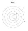
FIG. 3 is a diagram showing zone segments of the lamp block of the lamp annealer of the embodiment.
FIG. 4 is a flowchart showing an example of operations of the processing temperature control system of the embodiment.
PREFERRED EMBODIMENTS OF THE INVENTION
Now, concrete examples of the present invention will be described below. However, the present invention is not limited to the examples described below.
Referring to FIG. 1, a processing temperature control system according to an embodiment of the present invention includes an in-line host computer 11 for implementing an in-line lot control section and a data base of the work history effected until the previous step, and a control block of the lamp annealer 12.
The control block of the lamp annealer 12 includes a storage section 14 for storing data for one or more of the transistor characteristics, such as the threshold voltage (VT), breakdown voltage (BVDS) and operational speed (ION) of the transistors in the wafer, an input means 16 for inputting data to the storage section 14, a calculating section 15 for calculating the data, and a control section 13 for receiving the stored data from the storage section 14 and the calculating section 15 to control the lamp annealer 12. The arrows illustrated in FIG. 1 mean the directions of the information.
In addition, the lamp annealer 12 has a structure as a processing chamber and accessories thereof shown in FIG. 2. More specifically, the lamp annealer 12 includes a processing chamber 17 having a structure capable of being sealed from the open air during processing a wafer 25, a circular lamp or lamp block 18 including a plurality of annular zone segments 18 1 to 18 N arranged in a radial direction for heating respective areas of the wafer, a gas inlet port 19 for introducing a process gas to the processing chamber 17, a gas exhaust port 20 for exhausting the process gas from the processing chamber 17, a wafer support member 21 for supporting the wafer 25, a drive section 23 for rotating the wafer support member 21, and a plurality of pyrometers 22 1 to 22 N each for measuring the wafer temperature at a specified position on the bottom surface of the wafer 25.
The wafer 25 under processing is located on the wafer support member 21. The lamp block 18 is divided into “N” zone segments 18 1, 18 2, . . . 18 N , and can be adjusted in the output power of the lamp block for each of the zone segments 18 1, 18 2, . . . 18 N. In addition, the pyrometers 22 1, 22 2, 22 N are disposed corresponding to the zone segments 18 1, 18 2, . . . 18 N of the lamp block 18 in a one-to-one correspondence, whereby the pyrometers 22 1, 22 2, . . . 22 N monitor the wafer temperature for respective zone segments of the lamp block 18. FIG. 3 shows the top plan view of the zone segments of the lamp block 18, wherein annular zone segments 18 1, 18 2, . . . 18 N having a substantially equal width are arranged in a radial direction.
Next, an exemplified operation of the system will be described with reference to FIGS. 1 to 4 and Tables 1 and 2. In Tables 1 and 2, condition items include items which affect the transistor characteristics, such as gate length and the thickness of the gate side-wall film which are determined by the actual process conditions. “X” is the parameter for each item to be used for defining the specified transistor characteristic (or threshold voltage VT), and Y1 to Yn are design values or standard values for the respective items. In this example, it is assumed that the threshold voltage VT is affected by quadratic of the parameter for each item, as shown by the columns of the expression for VT.
| |
|
|
measured |
|
| item |
design value |
expression for VT |
value |
VT fluctuation |
| |
| item 1 |
Y1 |
a′X2 + b′X + c′ |
|
|
| item 2 |
Y2 |
a″X2 + b″X + c |
| item 3 |
Y3 |
a″′X2 + b″′X + c |
| item 4 |
Y4 |
a″″X2 + b″″X + c |
| — |
— |
— |
| — |
— |
— |
| — |
— |
— |
| item n |
Yn |
a(′)nX2 + b(′)nX + c |
| |
| |
design |
expression for |
measured |
|
| item |
value |
VT |
value |
VT fluctuation |
| |
| item 1 |
Y1 |
a′X2 + b′X + c |
S1 |
VT1 = a′S2 + b′S + |
| |
|
|
|
c − a′Y2 − b′Y − c |
| item 2 |
Y2 |
a″X2 + b″X + c |
S2 |
VT2 = a″S2 + b″S + |
| |
|
|
|
c − a″Y2 − b″Y − c |
| item 3 |
Y3 |
a″′X2 + b″′X + c |
S3 |
VT3 = ......... |
| item 4 |
Y4 |
a″″X2 + b″″X + c |
S4 |
VT4 = ......... |
| — |
— |
— |
— |
| — |
— |
— |
— |
| — |
— |
— |
— |
| item n |
Yn |
a(′)nX2 + b(′)nX + c |
Sn |
VTn = a(′)nS2 + b(′)n |
| |
|
|
|
S + c − a(′)nY2 − b(′)n |
| |
|
|
|
Y − c(′)n |
| |
In FIG. 4, when a wafer is introduced to each of specified work steps, the in-line host computer 11 recognizes the wafer (step 1) and transfers the lot code “A” thereof to the control section 13 of the lamp annealer 12 (step 2). The control section 13 retrieves, from the storage section 14, the matrix An′ shown by Table 1 corresponding to the final product defined by the lot code “A” (step 3). The lot code defines the type of the final product as well as the lot number of the wafer.
The matrix An′ includes columns for condition items (X1 to XN: such as the dimension of gate length, and the thickness of the side-wall film), the design values or standard values for the items, and relational expressions showing the relationships between the condition items and the specified item (VT) of the transistor characteristics. The columns for condition items, design values and the expressions for VT are filled beforehand with the data input by the external input means 16, whereas the remaining columns are blank at this stage.
The control section 13 requests the data for the blank columns of the matrix An′ from the in-line host computer 11, and the data S1 to Sn obtained by measurements in the respective work steps are transferred from the in-line host computer 11 to the control section 13. Then, some of the columns of the matrix Bn′ shown in Table 2 are filled (step 4) with the transferred data S1 to Sn.
The control section 13 transfers the matrix Bn′ to the calculating section 15, which calculates a VT fluctuation VT1, VT2, . . . VTn for each item (step 5). Based on these VT fluctuations VT1, VT2, . . . VTn of the respective items, the total fluctuation VT(total)=Σn=1˜nVTn is calculated (step 6).
Subsequently, a numerical expression (VT=cZ+d), wherein “Z” is the lamp anneal processing temperature, “c” and “d” are constants, is transferred from the storage section 14 to the calculating section 15 (step 7). The numerical expression is registered corresponding to the type of the final product defined by the lot code and shows the relationship between the lamp anneal processing temperature and the threshold voltage VT of the transistor. Then, the lamp anneal processing temperature is calculated based on the numerical expression and the total fluctuation VT(total) so as to cancel the total fluctuation VT(total) by selecting the calculated processing temperature (step 8).
The matrixes A1 to AN are prepared beforehand corresponding to respective zone segments of the lamp block 18, whereby the processing temperature for each zone segment is calculated based on the numerical expression and the total fluctuation. The calculated temperatures are delivered to the control section 13, which adjusts the output power of each zone segment for processing the wafer by selecting the calculated processing temperature for the lamp anneal processing temperature (step 9).
Thus, according to the present embodiment, by predicting the fluctuations of the transistor characteristic until the previous step prior to the lamp annealing step and changing the heat processing temperatures within the wafer surface, the in-plane variations of the characteristic can be reduced.
In the above embodiment, the calculation for VT and the processing temperature is conducted by assuming that the relationship between each condition item and VT is quadratic and the relationship between the lamp anneal temperature and VT is linear. However, The number of exponential order in the relational expression can be selected by conducting experiments. In addition, it is assumed in the above embodiment that the relational expression between each item and VT is not affected by the measurements for the other condition items. However, if a plurality of relational expressions for VT are input beforehand by the external input means for respective cases of the measurements of a specified condition item, the relational expression for VT may be automatically changed for calculation based on the actual measurement of the specified condition item.
In the above embodiment, the relational expression between the condition item and VT as well as the numerical expression between the lamp anneal processing temperature and VT are stored in the storage section 14 of the lamp annealer 12, and the calculation is conducted by the calculating section 15 in the lamp annealer 12. However, since a large amount of data for the measurements until the previous step must be downloaded from the in-line host computer 11 to the lamp annealer 12 in the present embodiment, there is some drawback that the throughput of the system is not satisfactory.
In an alternative, the functions of the storage section 14 and the calculating section 15 are allocated to the in-line host computer 11. In this configuration, the processing conditions can be determined before the lot is introduced to the lamp anneal step, whereby a higher through-put can be obtained.
According to the present invention, the processing condition, i.e., the in-plane temperatures of the wafer surface effected by the lamp annealer, can be automatically determined based on the work history of the wafer until the previous step, thereby allowing change of the processing condition so as to adjust the transistor characteristic of the final product. In other word, by predicting the fluctuations of the characteristic until the previous step and changing the processing temperatures within the wafer surface, the in-plane variations of the characteristic can be reduced.