US6466143B2 - Non-return-to-zero DAC using reference sine wave signals - Google Patents
Non-return-to-zero DAC using reference sine wave signals Download PDFInfo
- Publication number
- US6466143B2 US6466143B2 US09/824,565 US82456501A US6466143B2 US 6466143 B2 US6466143 B2 US 6466143B2 US 82456501 A US82456501 A US 82456501A US 6466143 B2 US6466143 B2 US 6466143B2
- Authority
- US
- United States
- Prior art keywords
- signal
- digital
- sin
- dac
- analog converter
- Prior art date
- Legal status (The legal status is an assumption and is not a legal conclusion. Google has not performed a legal analysis and makes no representation as to the accuracy of the status listed.)
- Expired - Lifetime
Links
Images


Classifications
-
- H—ELECTRICITY
- H03—ELECTRONIC CIRCUITRY
- H03M—CODING; DECODING; CODE CONVERSION IN GENERAL
- H03M3/00—Conversion of analogue values to or from differential modulation
- H03M3/30—Delta-sigma modulation
- H03M3/322—Continuously compensating for, or preventing, undesired influence of physical parameters
- H03M3/368—Continuously compensating for, or preventing, undesired influence of physical parameters of noise other than the quantisation noise already being shaped inherently by delta-sigma modulators
- H03M3/37—Compensation or reduction of delay or phase error
- H03M3/372—Jitter reduction
-
- H—ELECTRICITY
- H03—ELECTRONIC CIRCUITRY
- H03M—CODING; DECODING; CODE CONVERSION IN GENERAL
- H03M3/00—Conversion of analogue values to or from differential modulation
- H03M3/30—Delta-sigma modulation
- H03M3/39—Structural details of delta-sigma modulators, e.g. incremental delta-sigma modulators
- H03M3/40—Arrangements for handling quadrature signals, e.g. complex modulators
-
- H—ELECTRICITY
- H03—ELECTRONIC CIRCUITRY
- H03M—CODING; DECODING; CODE CONVERSION IN GENERAL
- H03M3/00—Conversion of analogue values to or from differential modulation
- H03M3/30—Delta-sigma modulation
- H03M3/50—Digital/analogue converters using delta-sigma modulation as an intermediate step
- H03M3/502—Details of the final digital/analogue conversion following the digital delta-sigma modulation
Definitions
- the present invention relates to a high resolution, high order delta signal digital-to-analog converter. Specifically, a feed forward DAC is disclosed for converting a digital signal to a low noise analog signal which minimizes the effects of clock jitter on the noise floor of the analog signal.
- Radio frequency communications systems such as cellular telephone systems employ significant amounts of digital processing to both transmit and receive signals.
- information is processed on a digital level and only at the final radio frequency carrier level is the signal converted to an analog signal.
- the analog signal is then mixed with an RF carrier of the cellular telephone system for transmission.
- the digital data processed below the radio frequency signal band is upwards to 16 bits wide.
- the high resolution digital signal may then be converted to a lower order bit signal using a digital signal modulator.
- the process of converting the digital signal to an analog signal introduces noise in the signal thereby limiting the resolution of the converted signal.
- the noise is strongly affected by the amount of phase jitter in the data being converted by the digital analog converter.
- Phase jitter on the incoming digital data to the DAC is the result of the phase jitter on the system clock which affects the digital data bit transitions producing the phase noise modulation.
- the phase noise modulation contributes to the noise floor of the resulting analog signal limiting the ability to obtain a high resolution of the analog signal level.
- the present invention is directed to a DAC which maintains the high resolution of an incoming digital signal which is converted into an analog signal.
- a non return to zero (NRZ) SIN digital-to-analog converter for converting a digital input signal to an analog signal.
- the NRZ SIN digital-to-analog converter provides an sine wave output in response to a first state of a digital signal proportional to 1+COS 2 ⁇ f(t), and in response to a second state of the digital signal, a sine wave signal proportional to ⁇ 1 ⁇ COS 2 ⁇ f(t).
- a second SIN digital to analog converter receives a delayed version of the digital signal.
- the output of the second SIN digital converter is phase shifted with respect to the output of the first sign digital converter, and the respective output signals are combined to produce a non-return to zero (NRZ) output voltage.
- the NRZ output voltage contains less high frequency content than produced by a return to zero (RZ) SIN DAC, and the only significant phase noise which results from phase jitter occurs during data transitions.
- FIG. 1 illustrates the typical delta signal digital-to-analog converter architecture in a radio telephone communication system
- FIG. 2A illustrates the ideal clock signal having no jitter
- FIG. 2B illustrates the clock signal which is subject to phase jitter
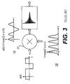
- FIG. 3 illustrates the architecture of a SIN DAC
- FIG. 4 illustrates the relative differences in signal error energy due to phase jitter on the digital input data and on the output signal of a SIN DAC
- FIG. 5 is a schematic representation of an RZ SIN DAC
- FIG. 6 illustrates the output of an RZ SIN DAC for different digital signals
- FIG. 7 represents a preferred embodiment of the invention for creating an NRZ SIN DAC
- FIG. 8 illustrates the output voltages from the individual SIN DACs and the composite NRZ output voltage of the NRZ SIN DAC
- FIG. 9 illustrates the respective outputs of the NRZ SIN DAC, and the RZ SIN DAC
- FIG. 10 illustrates the phase noise produced from data transitions of data being converted to an analog voltage
- FIG. 11 illustrates the difference in signal to noise ratio of between the NRZ SIN DAC and RZ SIN DAC.
- FIG. 1 illustrates a delta sigma digital-to-analog converter.
- the delta sigma digital-to-analog converter is included in the transmit chain of a wireless telephone communication device which is employed in the cellular telephone service.
- An interpolator 11 receives a digital signal representing information to be transmitted by the cellular telephone transmitter.
- the interpolator 11 converts the digital signal to a lower order digital signal and increases the data rate which is applied to a multibit digital delta signal modulator 12 .
- the delta sigma modulator provides noise shaping of the digital signal and forwards the lower order digital signal to a feed forward DAC 13 .
- the analog voltage produced by DAC 13 is supplied to a smoothing filter 14 which generates the analog signal for transmission on an RF carrier.
- Phase jitter accompanying the digital data is a result of a short term clock instability in the digital processing system.
- FIG. 2A shows an ideal clock, wherein during a transition, no change in the location of the rising and falling edge of the clock pulse is seen. Practically, however, a certain amount of instability always accompanies a clock pulse, as illustrated in FIG. 2 b .
- This instability in the clock signal edge is referred to as “jitter” and is also present on the data being converted, and is the source of phase noise derived from the feed forward DAC 13 .
- the resulting phase jitter produces a noise floor which limits the signal-to-noise ratio of the transmitted signal.
- the signal is received at the receiving side of a cellular telephone communication system and is reconverted to a digital signal having resolution limited by the noise floor accompanying the input signal.
- the SIN DAC is based on a pulse shaping process, wherein instead of providing a fixed DC level at the output of the DAC, the output energy is shaped sinusoidally, and data transitions occur only at the portion of a sine wave voltage which has a zero slope thereby reducing the sensitivity to clock jitter as will be explained with respect to FIG. 4 .
- the SIN DAC receives an input signal a(t) to a multiplier 17 input.
- a second input of the multiplier 17 receives a sine (cosine) voltage having a DC level associated with it.
- This composite signal may be represented by 1+COS (2 ⁇ ft).
- the result is a multiplication of the sine wave so that for positive values of a(t), the value of the output voltage of the SIN DAC is 1+COS(2 ⁇ ft), and for negative transitions, when the input data a(t) is a ⁇ 1, an output voltage of ⁇ 1 ⁇ COS(2 ⁇ ft) is produced.
- the sine wave signal is phase locked with the clock signal in circuitry (not shown), so that data transitions occur at the point the sine wave signal voltage is at approximately a zero slope which reduces the amount of phase noise added to the analog signal.
- FIG. 4 The effects of the SIN DAC output voltage on phase noise is illustrated in to FIG. 4 .
- a data transition occurs, switching between each of the signals 1+COS 2 ⁇ ft and ⁇ 1 ⁇ COS 2 ⁇ ft occurs.
- Changes in the data transition corresponding to changes in clock signal transitions shown in FIG. 2B, produce an output energy 24 which contributes noise.
- the noise energy 24 is considerably less than the noise energy 23 which is produced from the jitter which occurs in the edges of the digital data signal.
- FIG. 5 illustrates a schematic representation of a SIN DAC.
- An input sine wave signal is applied to the base of transistors 30 and 31 which are connected in a differential amplifier configuration.
- the sine signals produced from the collectors of transistors 31 and 30 are added with a DC offset voltage, representing +1 and ⁇ 1.
- the offset voltage is produced from transistors 34 and 39 , connected to respective voltage references 36 and 40 .
- Current sources 35 and 41 provide the operating current for transistors 34 and 39 .
- An emitter degeneration resistance 36 , 38 is connected between the respective pairs of differential transistors.
- the input data is applied to the bases of transistors 25 , 26 , and 28 , 29 .
- the collectors of transistors 26 and 28 produce one or the other of the cosine wave forms having a d.c. level of +1 or ⁇ 1 corresponding to one or the other states of the input data signal.
- FIG. 6 illustrates the output voltage from an RZ SIN DAC for different values of input digital data.
- the representation of FIG. 6 illustrates the output voltage as the input digital data changes with time.
- Each value of input digital data produces a series of sine waves above zero volts, which are the source of high frequency noise in the output voltage. Additionally, the sinusoidal voltage swings can produce signal artifacts if they are processed by later circuitry which has any significant nonlinearities.
- NRZ non-return to zero
- FIG. 7 an implementation in accordance with a preferred embodiment is shown which forms an NRZ output signal 53 from two RZ output signals 50 , 51 produced by RZ SIN DAC 43 and RZ SIN DAC 44 , previously described.
- Each of the SIN DACs 43 and 44 produce a sine voltage derived from sine (cosine) wave generator 45 .
- the output of SIN DAC 43 is delayed as a phase shift network 46 is connected between the source of sine voltage 45 and SIN DAC 43 providing a relative phase shift between SIN DACs 43 , 44 of approximately 180°.
- the input digital signal to SIN DAC 43 is delayed for one-half of a clock cycle period by delay circuit 41 .
- the combined output signals 50 , 51 , from SIN DAC 43 and SIN DAC 44 is illustrated in FIG. 8 .
- the composite signal 53 does not return to zero, except during a data transition. The effect is shown in FIG. 9, wherein the multiple voltage excursions between zero and either 1 or ⁇ 1 is avoided, except during the data transition edges.
- NRZ signal 53 therefore has significantly less high frequency content than the signals 50 , 51 produced by the RZ SIN DACs 43 , 44 .
- FIG. 10 illustrates the effects on noise produced due to the clock jitter.
- the analog output voltage is shown as a function of time, wherein the digital data values change over time to produce the different output values of analog voltage shown. The only significant contribution to phase noise occurs at the data transition edges.
- a comparison between the relative phase noise produced by an NRZ and RZ SIN DAC, expressed as a signal to noise ratio of the analog signal, is shown in FIG. 11 .
- the NRZ SIN DAC demonstrates significantly less noise over the amplitude of the output signal shown.
- the fact that the NRZ sin DAC has a noise response limited to data transitions can be demonstrated below:
- ⁇ 1 is the phase noise
- phase noise gets cancelled because there is a 180° ( ⁇ ) phase shift between sin DACs 60 , 61 .
- FIG. 7 contemplates combining the output of two RZ SIN DACs, it is of course possible to use four, or more SIN DACs, combining the outputs together to create an even smoother voltage waveform. In such a case, additional delays would be interposed between the digital signal and the SIN DACs. For instance, where four SIN DACs are used, each SIN DAC would receive a SIN voltage which is 90° shifted, and each digital signal would be delayed by one-fourth a clock period.
Abstract
Description
Claims (10)
Priority Applications (1)
| Application Number | Priority Date | Filing Date | Title |
|---|---|---|---|
| US09/824,565 US6466143B2 (en) | 2001-04-03 | 2001-04-03 | Non-return-to-zero DAC using reference sine wave signals |
Applications Claiming Priority (1)
| Application Number | Priority Date | Filing Date | Title |
|---|---|---|---|
| US09/824,565 US6466143B2 (en) | 2001-04-03 | 2001-04-03 | Non-return-to-zero DAC using reference sine wave signals |
Publications (2)
| Publication Number | Publication Date |
|---|---|
| US20020140593A1 US20020140593A1 (en) | 2002-10-03 |
| US6466143B2 true US6466143B2 (en) | 2002-10-15 |
Family
ID=25241731
Family Applications (1)
| Application Number | Title | Priority Date | Filing Date |
|---|---|---|---|
| US09/824,565 Expired - Lifetime US6466143B2 (en) | 2001-04-03 | 2001-04-03 | Non-return-to-zero DAC using reference sine wave signals |
Country Status (1)
| Country | Link |
|---|---|
| US (1) | US6466143B2 (en) |
Cited By (6)
| Publication number | Priority date | Publication date | Assignee | Title |
|---|---|---|---|---|
| US6573848B2 (en) * | 2001-03-09 | 2003-06-03 | Victor Company Of Japan, Ltd. | Modulation system using encoding tables and method therefor |
| US20030164782A1 (en) * | 2002-03-01 | 2003-09-04 | Kyle Stickle | Method and apparatus for electrical non-return to zero to return to zero conversion |
| US20080143570A1 (en) * | 2006-12-15 | 2008-06-19 | Telefonaktiebolaget Lm Ericsson (Publ) | Method and apparatus for feedback signal generation in sigma-delta analog-to-digital converters |
| US20100328124A1 (en) * | 2009-06-30 | 2010-12-30 | Mediatek Singapore Pte. Ltd. | Current steering digital-to-analog converter |
| US9319060B2 (en) * | 2014-07-17 | 2016-04-19 | Lattice Semiconductor Corporation | Frequency response compensation in a digital to analog converter |
| US9742428B2 (en) | 2015-07-17 | 2017-08-22 | Samsung Electronics Co., Ltd. | Delta sigma modulator for shaping noise and audio codec having the same |
Families Citing this family (4)
| Publication number | Priority date | Publication date | Assignee | Title |
|---|---|---|---|---|
| US6727832B1 (en) * | 2002-11-27 | 2004-04-27 | Cirrus Logic, Inc. | Data converters with digitally filtered pulse width modulation output stages and methods and systems using the same |
| US6778116B1 (en) * | 2003-02-25 | 2004-08-17 | Northrop Grumman Corporation | Switching DAC pulse encoding circuit |
| US8618969B2 (en) * | 2012-03-07 | 2013-12-31 | Telefonaktiebolaget L M Ericsson (Publ) | Low complexity high-speed multi-DAC system |
| US10439631B1 (en) * | 2018-12-27 | 2019-10-08 | Texas Instruments Incorporated | Radio-frequency digital-to-analog converter system |
Citations (10)
| Publication number | Priority date | Publication date | Assignee | Title |
|---|---|---|---|---|
| US4975699A (en) * | 1989-12-01 | 1990-12-04 | Hughes Aircraft Company | Error reduction method and apparatus for a direct digital synthesizer |
| US4983972A (en) | 1989-10-13 | 1991-01-08 | The United States Of America As Represented By The Secretary Of The Navy | Video delta modulation encoder |
| US5056118A (en) | 1989-05-16 | 1991-10-08 | Rockwell International Corporation | Method and apparatus for clock and data recovery with high jitter tolerance |
| US5528239A (en) | 1992-04-17 | 1996-06-18 | Crystal Semiconductor Corporation | Low noise transmission of output data from a delta-sigma modulator |
| US5557635A (en) | 1994-01-12 | 1996-09-17 | The United States Of America As Represented By The Secretary Of The Air Force | Voice encode/decode subsystem in a system for acquisition of test data using pulse code modulation |
| US5610606A (en) | 1993-07-21 | 1997-03-11 | Kabushiki Kaisha Toshiba | 1-bit D/A conversion circuit |
| US5701106A (en) * | 1995-06-06 | 1997-12-23 | Nokia Mobile Phones Ltd. | Method and modulator for modulating digital signal to higher frequency analog signal |
| US6114981A (en) | 1997-12-05 | 2000-09-05 | Kabushiki Kaisha Toshiba | D/A converter |
| US6121910A (en) | 1998-07-17 | 2000-09-19 | The Trustees Of Columbia University In The City Of New York | Frequency translating sigma-delta modulator |
| US6324236B1 (en) | 1997-05-15 | 2001-11-27 | Telefonaktiebolaget Lm Ericsson (Publ) | Phase detector arrangement |
-
2001
- 2001-04-03 US US09/824,565 patent/US6466143B2/en not_active Expired - Lifetime
Patent Citations (10)
| Publication number | Priority date | Publication date | Assignee | Title |
|---|---|---|---|---|
| US5056118A (en) | 1989-05-16 | 1991-10-08 | Rockwell International Corporation | Method and apparatus for clock and data recovery with high jitter tolerance |
| US4983972A (en) | 1989-10-13 | 1991-01-08 | The United States Of America As Represented By The Secretary Of The Navy | Video delta modulation encoder |
| US4975699A (en) * | 1989-12-01 | 1990-12-04 | Hughes Aircraft Company | Error reduction method and apparatus for a direct digital synthesizer |
| US5528239A (en) | 1992-04-17 | 1996-06-18 | Crystal Semiconductor Corporation | Low noise transmission of output data from a delta-sigma modulator |
| US5610606A (en) | 1993-07-21 | 1997-03-11 | Kabushiki Kaisha Toshiba | 1-bit D/A conversion circuit |
| US5557635A (en) | 1994-01-12 | 1996-09-17 | The United States Of America As Represented By The Secretary Of The Air Force | Voice encode/decode subsystem in a system for acquisition of test data using pulse code modulation |
| US5701106A (en) * | 1995-06-06 | 1997-12-23 | Nokia Mobile Phones Ltd. | Method and modulator for modulating digital signal to higher frequency analog signal |
| US6324236B1 (en) | 1997-05-15 | 2001-11-27 | Telefonaktiebolaget Lm Ericsson (Publ) | Phase detector arrangement |
| US6114981A (en) | 1997-12-05 | 2000-09-05 | Kabushiki Kaisha Toshiba | D/A converter |
| US6121910A (en) | 1998-07-17 | 2000-09-19 | The Trustees Of Columbia University In The City Of New York | Frequency translating sigma-delta modulator |
Non-Patent Citations (5)
| Title |
|---|
| Flikkema, Paul G., and Davisson, Lee D., Detection of Baseband Signals Using a Delta Modulator, May 1988, IEEE Transactions on Information Theory, vol. 34, No. 3, pp 537-543. |
| Flikkema, Paul G.; Davisson, Lee D. "Detection of Baseband Signals Using a Delta Modulator", IEEE Transactions on Information Theory, vol. 335, No. 3, May 1988, pp. 537-543. |
| O. Shoaei and W.M. Snelgrove, "Design and Implementatioin of a Tunable 40 MHz-70 MHz Gm-C Bandpass DELTAΕModulator," Jul. 1997, IEEE Transactions on Circuits and Systems-II: Analog and Digital Signal Processing, vol. 44, No. 7. |
| O. Shoaei and W.M. Snelgrove, "Design and Implementatioin of a Tunable 40 MHz-70 MHz Gm-C Bandpass ΔΕModulator," Jul. 1997, IEEE Transactions on Circuits and Systems-II: Analog and Digital Signal Processing, vol. 44, No. 7. |
| W. Gao and W.M. Snelgrove, "A 950-MHz IF Second-Order Integrated LC Bandpass Delta-Sigma Modulator," May 1998, IEEE Journal of Solid-State Circuits, vol. 33, No. 5. |
Cited By (11)
| Publication number | Priority date | Publication date | Assignee | Title |
|---|---|---|---|---|
| US6573848B2 (en) * | 2001-03-09 | 2003-06-03 | Victor Company Of Japan, Ltd. | Modulation system using encoding tables and method therefor |
| US6690308B2 (en) | 2001-03-09 | 2004-02-10 | Victor Company Of Japan, Ltd. | Computer program for implementing a modulation method and a demodulation method therefor |
| US20030164782A1 (en) * | 2002-03-01 | 2003-09-04 | Kyle Stickle | Method and apparatus for electrical non-return to zero to return to zero conversion |
| US6680679B2 (en) * | 2002-03-01 | 2004-01-20 | Anritsu Company | Method and apparatus for electrical conversion of non-return to zero encoded signal to return to zero encoded signal |
| US20080143570A1 (en) * | 2006-12-15 | 2008-06-19 | Telefonaktiebolaget Lm Ericsson (Publ) | Method and apparatus for feedback signal generation in sigma-delta analog-to-digital converters |
| US7414557B2 (en) | 2006-12-15 | 2008-08-19 | Telefonaktiebolaget Lm Ericsson (Publ) | Method and apparatus for feedback signal generation in sigma-delta analog-to-digital converters |
| US20100328124A1 (en) * | 2009-06-30 | 2010-12-30 | Mediatek Singapore Pte. Ltd. | Current steering digital-to-analog converter |
| US7994957B2 (en) * | 2009-06-30 | 2011-08-09 | Mediatek Singapore Pte. Ltd. | Current steering digital-to-analog converter |
| JP2012531864A (en) * | 2009-06-30 | 2012-12-10 | メディアテック シンガポール ピーティーイー エルティーディー | Current steering digital-to-analog converter |
| US9319060B2 (en) * | 2014-07-17 | 2016-04-19 | Lattice Semiconductor Corporation | Frequency response compensation in a digital to analog converter |
| US9742428B2 (en) | 2015-07-17 | 2017-08-22 | Samsung Electronics Co., Ltd. | Delta sigma modulator for shaping noise and audio codec having the same |
Also Published As
| Publication number | Publication date |
|---|---|
| US20020140593A1 (en) | 2002-10-03 |
Similar Documents
| Publication | Publication Date | Title |
|---|---|---|
| US5534827A (en) | Modulator | |
| US6462687B1 (en) | High performance delta sigma ADC using a feedback NRZ sin DAC | |
| US5767750A (en) | Modulator | |
| FI102930B (en) | A transmitter comprising an electronic arrangement for generating a modulated carrier signal | |
| CA2160592A1 (en) | Balanced modulator-transmitter | |
| US20030118143A1 (en) | Direct modulation architecture for amplitude and phase modulated signals in multi-mode signal transmission | |
| US20020131529A1 (en) | Digital modulator and digital demodular | |
| JPS60112344A (en) | Radio wave receiver and demodulating method | |
| US20050062529A1 (en) | Adaptive wideband digital amplifier for linearly modulated signal amplification and transmission | |
| US7352311B2 (en) | Continuous time noise shaping analog-to-digital converter | |
| US6466143B2 (en) | Non-return-to-zero DAC using reference sine wave signals | |
| CA2213156A1 (en) | One bit digital quadrature vector modulator | |
| US6754287B2 (en) | Method and apparatus for producing a modulated signal | |
| US7403066B2 (en) | Method and system for creating a spectral null in a switching amplifier | |
| US7280003B2 (en) | Modulation device and transmitter comprising such a device | |
| US6940920B2 (en) | Multiplier arrangement, signal modulator and transmitter | |
| US6778116B1 (en) | Switching DAC pulse encoding circuit | |
| US4825452A (en) | Digital FSK demodulator | |
| US6320529B1 (en) | A/D conversion apparatus and a radio apparatus | |
| US7002425B2 (en) | Pulse modulation | |
| US20040061634A1 (en) | D/a converter with high jitter resistance | |
| US7880656B2 (en) | RF chip including shared converter and transceiver including the RF chip | |
| CN104980386B (en) | Method and apparatus for providing crosspoint information | |
| US11211908B2 (en) | Power amplifier and demodulator | |
| US9319076B2 (en) | Modulation method for improving signal conversion gain and high-gain modulator thereof |
Legal Events
| Date | Code | Title | Description |
|---|---|---|---|
| AS | Assignment |
Owner name: INTERNATIONAL BUSINESS MACHINES CORPORATION, NEW Y Free format text: ASSIGNMENT OF ASSIGNORS INTEREST;ASSIGNORS:ESHRAGHI, ARIA;GANTI, RAMKISHORE;REEL/FRAME:011993/0928 Effective date: 20010629 |
|
| STCF | Information on status: patent grant |
Free format text: PATENTED CASE |
|
| AS | Assignment |
Owner name: MEDIATEK INC., TAIWAN Free format text: ASSIGNMENT OF ASSIGNORS INTEREST;ASSIGNOR:INTERNATIONAL BUSINESS MACHINES CORPORATION;REEL/FRAME:017045/0559 Effective date: 20050930 |
|
| FPAY | Fee payment |
Year of fee payment: 4 |
|
| FEPP | Fee payment procedure |
Free format text: PAYOR NUMBER ASSIGNED (ORIGINAL EVENT CODE: ASPN); ENTITY STATUS OF PATENT OWNER: LARGE ENTITY Free format text: PAYER NUMBER DE-ASSIGNED (ORIGINAL EVENT CODE: RMPN); ENTITY STATUS OF PATENT OWNER: LARGE ENTITY |
|
| FPAY | Fee payment |
Year of fee payment: 8 |
|
| FPAY | Fee payment |
Year of fee payment: 12 |
|
| AS | Assignment |
Owner name: XUESHAN TECHNOLOGIES INC., CANADA Free format text: ASSIGNMENT OF ASSIGNORS INTEREST;ASSIGNOR:MEDIATEK INC.;REEL/FRAME:055443/0818 Effective date: 20201223 |