US6455177B1 - Stabilization of GMR devices - Google Patents
Stabilization of GMR devices Download PDFInfo
- Publication number
- US6455177B1 US6455177B1 US09/454,085 US45408599A US6455177B1 US 6455177 B1 US6455177 B1 US 6455177B1 US 45408599 A US45408599 A US 45408599A US 6455177 B1 US6455177 B1 US 6455177B1
- Authority
- US
- United States
- Prior art keywords
- layer
- ferromagnetic
- gmr
- layers
- coupler
- Prior art date
- Legal status (The legal status is an assumption and is not a legal conclusion. Google has not performed a legal analysis and makes no representation as to the accuracy of the status listed.)
- Expired - Lifetime
Links
Images


Classifications
-
- G—PHYSICS
- G01—MEASURING; TESTING
- G01R—MEASURING ELECTRIC VARIABLES; MEASURING MAGNETIC VARIABLES
- G01R33/00—Arrangements or instruments for measuring magnetic variables
- G01R33/02—Measuring direction or magnitude of magnetic fields or magnetic flux
- G01R33/06—Measuring direction or magnitude of magnetic fields or magnetic flux using galvano-magnetic devices
- G01R33/09—Magnetoresistive devices
- G01R33/093—Magnetoresistive devices using multilayer structures, e.g. giant magnetoresistance sensors
-
- B—PERFORMING OPERATIONS; TRANSPORTING
- B82—NANOTECHNOLOGY
- B82Y—SPECIFIC USES OR APPLICATIONS OF NANOSTRUCTURES; MEASUREMENT OR ANALYSIS OF NANOSTRUCTURES; MANUFACTURE OR TREATMENT OF NANOSTRUCTURES
- B82Y10/00—Nanotechnology for information processing, storage or transmission, e.g. quantum computing or single electron logic
-
- B—PERFORMING OPERATIONS; TRANSPORTING
- B82—NANOTECHNOLOGY
- B82Y—SPECIFIC USES OR APPLICATIONS OF NANOSTRUCTURES; MEASUREMENT OR ANALYSIS OF NANOSTRUCTURES; MANUFACTURE OR TREATMENT OF NANOSTRUCTURES
- B82Y25/00—Nanomagnetism, e.g. magnetoimpedance, anisotropic magnetoresistance, giant magnetoresistance or tunneling magnetoresistance
-
- G—PHYSICS
- G11—INFORMATION STORAGE
- G11B—INFORMATION STORAGE BASED ON RELATIVE MOVEMENT BETWEEN RECORD CARRIER AND TRANSDUCER
- G11B5/00—Recording by magnetisation or demagnetisation of a record carrier; Reproducing by magnetic means; Record carriers therefor
- G11B5/127—Structure or manufacture of heads, e.g. inductive
- G11B5/33—Structure or manufacture of flux-sensitive heads, i.e. for reproduction only; Combination of such heads with means for recording or erasing only
- G11B5/39—Structure or manufacture of flux-sensitive heads, i.e. for reproduction only; Combination of such heads with means for recording or erasing only using magneto-resistive devices or effects
- G11B5/3903—Structure or manufacture of flux-sensitive heads, i.e. for reproduction only; Combination of such heads with means for recording or erasing only using magneto-resistive devices or effects using magnetic thin film layers or their effects, the films being part of integrated structures
- G11B5/3906—Details related to the use of magnetic thin film layers or to their effects
- G11B5/3929—Disposition of magnetic thin films not used for directly coupling magnetic flux from the track to the MR film or for shielding
- G11B5/3935—Flux closure films not being part of the track flux guides
- G11B5/3941—Flux closure films not being part of the track flux guides the flux closure films being used for providing a closed magnetic circuit to the MR film
-
- H—ELECTRICITY
- H10—SEMICONDUCTOR DEVICES; ELECTRIC SOLID-STATE DEVICES NOT OTHERWISE PROVIDED FOR
- H10N—ELECTRIC SOLID-STATE DEVICES NOT OTHERWISE PROVIDED FOR
- H10N50/00—Galvanomagnetic devices
- H10N50/10—Magnetoresistive devices
-
- G—PHYSICS
- G11—INFORMATION STORAGE
- G11B—INFORMATION STORAGE BASED ON RELATIVE MOVEMENT BETWEEN RECORD CARRIER AND TRANSDUCER
- G11B5/00—Recording by magnetisation or demagnetisation of a record carrier; Reproducing by magnetic means; Record carriers therefor
- G11B2005/0002—Special dispositions or recording techniques
- G11B2005/0005—Arrangements, methods or circuits
- G11B2005/0008—Magnetic conditionning of heads, e.g. biasing
-
- G—PHYSICS
- G11—INFORMATION STORAGE
- G11B—INFORMATION STORAGE BASED ON RELATIVE MOVEMENT BETWEEN RECORD CARRIER AND TRANSDUCER
- G11B5/00—Recording by magnetisation or demagnetisation of a record carrier; Reproducing by magnetic means; Record carriers therefor
- G11B5/127—Structure or manufacture of heads, e.g. inductive
- G11B5/33—Structure or manufacture of flux-sensitive heads, i.e. for reproduction only; Combination of such heads with means for recording or erasing only
- G11B5/39—Structure or manufacture of flux-sensitive heads, i.e. for reproduction only; Combination of such heads with means for recording or erasing only using magneto-resistive devices or effects
- G11B2005/3996—Structure or manufacture of flux-sensitive heads, i.e. for reproduction only; Combination of such heads with means for recording or erasing only using magneto-resistive devices or effects large or giant magnetoresistive effects [GMR], e.g. as generated in spin-valve [SV] devices
-
- G—PHYSICS
- G11—INFORMATION STORAGE
- G11B—INFORMATION STORAGE BASED ON RELATIVE MOVEMENT BETWEEN RECORD CARRIER AND TRANSDUCER
- G11B5/00—Recording by magnetisation or demagnetisation of a record carrier; Reproducing by magnetic means; Record carriers therefor
- G11B5/127—Structure or manufacture of heads, e.g. inductive
- G11B5/33—Structure or manufacture of flux-sensitive heads, i.e. for reproduction only; Combination of such heads with means for recording or erasing only
- G11B5/39—Structure or manufacture of flux-sensitive heads, i.e. for reproduction only; Combination of such heads with means for recording or erasing only using magneto-resistive devices or effects
- G11B5/3903—Structure or manufacture of flux-sensitive heads, i.e. for reproduction only; Combination of such heads with means for recording or erasing only using magneto-resistive devices or effects using magnetic thin film layers or their effects, the films being part of integrated structures
- G11B5/3906—Details related to the use of magnetic thin film layers or to their effects
- G11B5/3916—Arrangements in which the active read-out elements are coupled to the magnetic flux of the track by at least one magnetic thin film flux guide
-
- Y—GENERAL TAGGING OF NEW TECHNOLOGICAL DEVELOPMENTS; GENERAL TAGGING OF CROSS-SECTIONAL TECHNOLOGIES SPANNING OVER SEVERAL SECTIONS OF THE IPC; TECHNICAL SUBJECTS COVERED BY FORMER USPC CROSS-REFERENCE ART COLLECTIONS [XRACs] AND DIGESTS
- Y10—TECHNICAL SUBJECTS COVERED BY FORMER USPC
- Y10T—TECHNICAL SUBJECTS COVERED BY FORMER US CLASSIFICATION
- Y10T428/00—Stock material or miscellaneous articles
- Y10T428/11—Magnetic recording head
- Y10T428/1107—Magnetoresistive
- Y10T428/1121—Multilayer
- Y10T428/1129—Super lattice [e.g., giant magneto resistance [GMR] or colossal magneto resistance [CMR], etc.]
-
- Y—GENERAL TAGGING OF NEW TECHNOLOGICAL DEVELOPMENTS; GENERAL TAGGING OF CROSS-SECTIONAL TECHNOLOGIES SPANNING OVER SEVERAL SECTIONS OF THE IPC; TECHNICAL SUBJECTS COVERED BY FORMER USPC CROSS-REFERENCE ART COLLECTIONS [XRACs] AND DIGESTS
- Y10—TECHNICAL SUBJECTS COVERED BY FORMER USPC
- Y10T—TECHNICAL SUBJECTS COVERED BY FORMER US CLASSIFICATION
- Y10T428/00—Stock material or miscellaneous articles
- Y10T428/12—All metal or with adjacent metals
- Y10T428/12493—Composite; i.e., plural, adjacent, spatially distinct metal components [e.g., layers, joint, etc.]
- Y10T428/125—Deflectable by temperature change [e.g., thermostat element]
- Y10T428/12507—More than two components
-
- Y—GENERAL TAGGING OF NEW TECHNOLOGICAL DEVELOPMENTS; GENERAL TAGGING OF CROSS-SECTIONAL TECHNOLOGIES SPANNING OVER SEVERAL SECTIONS OF THE IPC; TECHNICAL SUBJECTS COVERED BY FORMER USPC CROSS-REFERENCE ART COLLECTIONS [XRACs] AND DIGESTS
- Y10—TECHNICAL SUBJECTS COVERED BY FORMER USPC
- Y10T—TECHNICAL SUBJECTS COVERED BY FORMER US CLASSIFICATION
- Y10T428/00—Stock material or miscellaneous articles
- Y10T428/12—All metal or with adjacent metals
- Y10T428/12493—Composite; i.e., plural, adjacent, spatially distinct metal components [e.g., layers, joint, etc.]
- Y10T428/125—Deflectable by temperature change [e.g., thermostat element]
- Y10T428/12514—One component Cu-based
Definitions
- the present invention relates to giant magnetoresitive (GMR) devices and more particularly to means for stabilizing GMR devices.
- the edges of a GMR stack must be stabilized to ensure that the magnetization of the edges does not rotate when exposed to an applied field. If the magnetization at the edges of a GMR stack moves during operation, this leads to noise which makes data recovery difficult or impossible.
- an oxidation process was used to provide stability. During the oxidation process, material near the edges of a GMR stack is transformed into an oxide, which helps to maintain the stability of the device. The result of oxidizing the material at the device edges appears to be an increase in the coercivity of these regions.
- the oxide may include some antiferromagnetic components that couple with the device edges, thereby pinning the magnetization of the device edges in a single direction. Additional steps are also typically performed during the oxidation process such as annealing. The annealing may be performed in the presence of a field.
- U.S. Pat. No. 5,756,366, entitled “MAGNETIC HARDENING OF BIT EDGES OF MAGNETORESISTIVE RAM” (the '366 patent) describes oxidation of device edges in a magnetoresitive RAM.
- the '366 patent discloses that the edges 23 of magnetic layers 20′ and 24′ are cleaned and then oxidized by placing the wafer in an oxygen plasma for a length of time.
- Several hundred to a thousand angstroms of magnetic material are oxidized as shown by the crosshatched portions 25 shown in FIG. 6 of the '366 patent.
- the cross-hatched edge portions 25 are magnetically harder than the inner portion of magnetic layers 20′ and 24′.
- the higher coercivity level of oxidized edge portions 25 acts to prevent bit edge reversal in the final magnetoresistive RAM device.
- the prior art therefore, discloses the transformation of the material at the edges of a device.
- the prior art does not disclose the deposition of additional layers on the device edges to provide stability. Such additional layers are desirable because they couple strongly with the device edges, and help to ensure that the device's edges do not rotate in the presence of an external field.
- a stabilized GMR device includes a GMR stack having a first and a second edge. Stabilization means are positioned adjacent to the first and the second edge of the GMR stack for stabilizing the GMR stack.
- the GMR stack includes a first layer of ferromagnetic material and a second layer of ferromagnetic material. A spacer layer is positioned between the first and the second ferromagnetic layers. A buffer layer is positioned adjacent to the first magnetic layer and a cap layer is positioned adjacent to the second ferromagnetic layer.
- the stabilization means include a first coupler layer positioned adjacent to the first edge of the GMR stack and a second coupler layer positioned adjacent to the second edge of the GMR stack. The stabilization means also include a first ferromagnetic layer positioned adjacent to the first coupler layer and a second ferromagnetic layer positioned adjacent to the second coupler layer.
- the stabilization means couples strongly anti-parallel to the ferromagnetic layers of the GMR stack, thereby effectively “hardening” the edges of the GMR stack, and making them less susceptible to reversal in an applied field.
- the stabilization means may be used to stabilize folded VGMR read heads, single VGMR read heads, GMR MRAM devices or other similar devices.
- FIG. 1 shows a prior art GMR stack.
- FIG. 2 shows a top view of the GMR stack shown in FIG. 1 .
- FIG. 3 shows a GMR stack with means for stabilization according to the present invention.
- FIG. 4 shows a top view of the GMR stack shown in FIG. 3 including means for stabilization according to the present invention.
- FIG. 5 shows a cross sectional view of a first embodiment of a folded VGMR read head.
- FIG. 6 shows a cross sectional view of second embodiment of a folded VGMR read head.
- FIG. 7 shows a cross sectional view of single VGMR read head.
- FIG. 1 shows a prior art GMR stack 10 .
- GMR stack 10 includes cap layer 12 , first ferromagnetic layer 14 , spacer layer 16 , second ferromagnetic layer 18 and buffer layer 20 .
- Cap layer 12 and buffer layer 20 are preferably Ta, TaN, or NiFeCr.
- Cap layer 12 and buffer layer 20 may alternatively comprise multilayer structures.
- Cap layer 12 protects the rest of the layers from oxidation.
- Buffer layer 20 facilitates an appropriate texture for the films deposited on it.
- Ferromagnetic layers 14 and 18 may either be a single layer magnetic film or a bi-layer such as NiFeCo/Co, NiFeCo/CoFe, NiFe/Co, NiFe/CoFe, where the Co-rich layer is located at the interface with spacer layer 16 to enhance GMR.
- Spacer layer 16 is preferably Cu.
- the configuration of GMR stack shown in FIG. 1 is typically used in a VGMR read head, which is discussed below with respect to FIGS. 5-7.
- a bias current is applied to GMR stack 10 in a direction perpendicular to the paper and into GMR stack 10 as represented by the encircled “X” shown on spacer layer 16 .
- the current applied through GMR stack 10 generates a field that acts in opposite directions on each of the two ferromagnetic layers 14 and 18 , “scissoring” their magnetizations apart as illustrated by the arrows on these layers.
- GMR stack 10 is in a high resistance state.
- FIG. 2 shows a top view of GMR stack 10 .
- the bias current through GMR stack 10 is represented by arrow 30 .
- Arrow 36 represents the magnetic flux from a magnetic medium.
- the magnetization in the center of GMR stack 10 is biased or scissored as indicated by crossed arrows 34 .
- other factors contribute to the bias of the device. For example, the patterning of ferromagnetic layers 14 and 18 leads to a shape anisotropy effect, causing the magnetizations to tend to align longitudinally. Therefore, the magnetizations of ferromagnetic layers 14 and 18 are not exactly anti-parallel, but are scissored as shown by crossed arrows 34 .
- the magnetizations of ferromagnetic layers 14 and 18 are preferably biased about 90 degrees apart.
- the magnetization near the right and left edges of GMR stack 10 is pinned due to high demagnetization fields.
- Arrows 32 A and 32 B represent the magnetization direction at the right and left edges of GMR stack 10 .
- the center magnetization in GMR stack 10 is the portion that responds to a signal from a magnetic medium.
- the angle between the magnetizations of ferromagnetic layers 14 and 18 changes based on the polarity of the magnetic flux 36 from a magnetic medium.
- One polarity will cause the magnetizations to spread farther apart, thereby increasing the resistance of the device.
- the opposite polarity causes the magnetizations to come closer together, thereby decreasing the resistance.
- the change in resistance is sensed to determine the data content of the magnetic media.
- the magnetization at the device edges ideally remains nearly fixed for a stable sensor response. If a high enough field is applied to the device, however, a portion of the edge magnetization will reverse, and the device will become unstable.
- FIG. 3 shows GMR stack 50 , which includes means for stabilization according to the present invention.
- GMR stack 50 includes cap layer 12 , first ferromagnetic layer 14 , spacer layer 16 , second ferromagnetic layer 18 and buffer layer 20 .
- Coupler layers 54 A and 54 B are deposited on first edge 31 A and second edge 31 B, respectively, of GMR stack 50 .
- Coupler layers 54 are preferably a strong anti-parallel coupler material such as Ru.
- Alternative materials for coupler layers 54 include copper, gold, silver and iridium, but Ru has the strongest anti-parallel coupling properties.
- Coupler layers 54 are preferably about 4-15 ⁇ thick.
- Ferromagnetic layers 52 A and 52 B are deposited adjacent to coupler layers 54 A and 54 B, respectively.
- Ferromagnetic layers 52 are preferably one of Co, NiFe, NiFeCo, or combinations of these materials. Ferromagnetic layers 52 are preferably about 20-100 ⁇ thick.
- FIG. 4 shows a top view of GMR stack 50 , including means for stabilization according to the present invention.
- the anti-parallel coupling between ferromagnetic layers 52 A- 52 B and GMR stack 50 at device edges 31 A and 31 B is represented in FIG. 4 by arrows on these regions.
- the coupling effectively “hardens” the edges 31 A and 31 B of GMR stack 50 , making them less susceptible to reversal in an applied field, and increasing the stability of the device.
- Deposition of ferromagnetic layers 52 and coupler layers 54 occurs after GMR stack 50 is patterned.
- Deposition of ferromagnetic layers 52 and coupler layers 54 on the edges of GMR stack 50 can be accomplished by a technique such as sputtering or ion beam deposition at a high angle.
- the field area is then etched directional in a self-aligned process to leave material selectively on the high angle sidewalls.
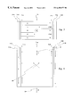
- FIG. 5 shows a cross-sectional view of a first embodiment of a folded VGMR read head.
- VGMR read head 60 includes top shield 62 , conductor 64 , second GMR stack 66 , gap material 67 , back contacts 68 , spacer 70 , first GMR stack 72 and bottom shield 74 .
- Conductor 64 may be a continuation of second GMR stack 66 .
- GMR stacks 66 and 72 are separated by spacer 70 .
- Spacer 70 is preferably silicon nitride, although other dielectric materials with a high breakdown voltage may be used.
- Shields 62 and 74 are recessed away from GMR stacks 66 and 72 , and separated therefrom by gap material 67 .
- Gap material 67 is preferably alumina or silicon nitride.
- the air bearing surface (ABS) 76 is also shown in FIG. 5 .
- GMR stacks 66 and 72 are configured in a folded structure.
- First GMR stack 72 has a resistance R 1 and second GMR stack 66 has a resistance R 2 .
- R 1 and R 2 respond in the same sense to an applied field.
- Contact is made to GMR stacks 66 and 72 independently at the back of read head 60 by back contacts 68 .
- Read head 60 may be either a two or three contact device. Current flows from one of back contacts 68 , through second GMR stack 66 , through conductor 64 , and back through first GMR stack 72 to a second one of back contacts 68 .
- First GMR stack 72 and second GMR stack 66 are essentially two resistors in series, which results in a higher resistivity and higher output signal than a parallel GMR stack configuration or a single GMR stack configuration.
- FIG. 6 shows a cross-sectional view of a second embodiment of a folded VGMR read head.
- Read head 80 includes top shield 82 , front contact 84 , second GMR stack 86 , spacer 88 , gap material 89 , back contacts 90 , first GMR stack 92 and bottom shield 94 .
- First GMR stack 92 has resistance R 1 and second GMR stack 86 has resistance R 2 .
- R 1 and R 2 respond in opposite senses to an applied field.
- GMR stacks 86 and 92 are shorted at ABS 76 and grounded.
- a differential signal is sensed in read head 80 as in a dual stripe magnetoresistive (DSMR) head.
- DSMR dual stripe magnetoresistive
- FIG. 7 shows a cross-sectional view of a single VGMR read head.
- Read head 100 includes top shield 102 , front contact 104 , GMR stack 106 , gap material 107 , back contact 108 and bottom shield 110 .
- front contact 104 also makes contact with bottom shield 110 .
- front contact 104 could be in electrical contact with top shield 102 .
- Read head 100 is a less complex design than read heads 60 and 80 , and is easier to build. The use of a single GMR stack results in lower resistance, a lower signal, and lower noise than a dual GMR stack design.
- the stabilization layers i.e., ferromagnetic layers 52 and coupler layers 54
- the stabilization technique of the present invention may also be used to stabilize other devices such as GMR MRAM (GMR magnetoresistive access memory) or magnetic field sensors.
Abstract
Description
Claims (17)
Priority Applications (2)
| Application Number | Priority Date | Filing Date | Title |
|---|---|---|---|
| US09/454,085 US6455177B1 (en) | 1999-10-05 | 1999-12-03 | Stabilization of GMR devices |
| US10/179,119 US6709696B2 (en) | 1999-10-05 | 2002-06-25 | Stabilization of GMR devices |
Applications Claiming Priority (2)
| Application Number | Priority Date | Filing Date | Title |
|---|---|---|---|
| US15787799P | 1999-10-05 | 1999-10-05 | |
| US09/454,085 US6455177B1 (en) | 1999-10-05 | 1999-12-03 | Stabilization of GMR devices |
Related Child Applications (1)
| Application Number | Title | Priority Date | Filing Date |
|---|---|---|---|
| US10/179,119 Division US6709696B2 (en) | 1999-10-05 | 2002-06-25 | Stabilization of GMR devices |
Publications (1)
| Publication Number | Publication Date |
|---|---|
| US6455177B1 true US6455177B1 (en) | 2002-09-24 |
Family
ID=26854556
Family Applications (2)
| Application Number | Title | Priority Date | Filing Date |
|---|---|---|---|
| US09/454,085 Expired - Lifetime US6455177B1 (en) | 1999-10-05 | 1999-12-03 | Stabilization of GMR devices |
| US10/179,119 Expired - Lifetime US6709696B2 (en) | 1999-10-05 | 2002-06-25 | Stabilization of GMR devices |
Family Applications After (1)
| Application Number | Title | Priority Date | Filing Date |
|---|---|---|---|
| US10/179,119 Expired - Lifetime US6709696B2 (en) | 1999-10-05 | 2002-06-25 | Stabilization of GMR devices |
Country Status (1)
| Country | Link |
|---|---|
| US (2) | US6455177B1 (en) |
Cited By (12)
| Publication number | Priority date | Publication date | Assignee | Title |
|---|---|---|---|---|
| US20020023338A1 (en) * | 2000-07-27 | 2002-02-28 | Seigler Michael Allen | Method for making a magnetoresistive sensor |
| US6552554B1 (en) * | 2001-12-06 | 2003-04-22 | The United States Of America As Represented By The Secretary Of The Navy | Testing current perpendicular to plane giant magnetoresistance multilayer devices |
| US6709696B2 (en) * | 1999-10-05 | 2004-03-23 | Seagate Technology Llc | Stabilization of GMR devices |
| US6798690B1 (en) | 2004-01-10 | 2004-09-28 | Honeywell International Inc. | Magnetic switching with expanded hard-axis magnetization volume at magnetoresistive bit ends |
| US20040252414A1 (en) * | 2003-06-12 | 2004-12-16 | Seagate Technology Llc | Magnetoresistive sensor with reduced operating temperature |
| US20050152181A1 (en) * | 2004-01-10 | 2005-07-14 | Honeywell International Inc. | Tunneling anisotropic magnetoresistive device and method of operation |
| US20070109839A1 (en) * | 2005-11-14 | 2007-05-17 | Honeywell International Inc. | MRAM read sequence using canted bit magnetization |
| US20070188942A1 (en) * | 2006-02-14 | 2007-08-16 | Beach Robert S | Tunnel MR head with closed-edge laminated free layer |
| US20070247897A1 (en) * | 2006-04-21 | 2007-10-25 | Honeywell International Inc. | Partitioned random access and read only memory |
| US20070272036A1 (en) * | 2006-05-25 | 2007-11-29 | Honeywell International Inc. | Two-element magnetic memory cell |
| US20070279970A1 (en) * | 2006-06-02 | 2007-12-06 | Honeywell International Inc. | Nonvolatile memory with data clearing functionality |
| US20090073755A1 (en) * | 2006-03-15 | 2009-03-19 | Honeywell International Inc. | MRAM read bit with askew fixed layer |
Families Citing this family (5)
| Publication number | Priority date | Publication date | Assignee | Title |
|---|---|---|---|---|
| US8397998B1 (en) | 1999-10-23 | 2013-03-19 | Ultracard, Inc. | Data storage device, apparatus and method for using same |
| US7487908B1 (en) * | 1999-10-23 | 2009-02-10 | Ultracard, Inc. | Article having an embedded accessible storage member, apparatus and method for using same |
| US6738235B1 (en) * | 2000-03-24 | 2004-05-18 | Seagate Technology Llc | Structures and materials to stabilize active layers in VGMR head using AFM transverse bias |
| US7251110B2 (en) * | 2005-01-18 | 2007-07-31 | Hitachi Global Storage Technologies Netherlands B.V. | GMR sensor having layers treated with nitrogen for increased magnetoresistance |
| US20110200845A1 (en) * | 2010-02-16 | 2011-08-18 | Seagate Technology Llc | Current perpendicular to the plane reader with improved giant magneto-resistance |
Citations (15)
| Publication number | Priority date | Publication date | Assignee | Title |
|---|---|---|---|---|
| US5159513A (en) * | 1991-02-08 | 1992-10-27 | International Business Machines Corporation | Magnetoresistive sensor based on the spin valve effect |
| US5206590A (en) * | 1990-12-11 | 1993-04-27 | International Business Machines Corporation | Magnetoresistive sensor based on the spin valve effect |
| US5251170A (en) | 1991-11-04 | 1993-10-05 | Nonvolatile Electronics, Incorporated | Offset magnetoresistive memory structures |
| US5420819A (en) | 1992-09-24 | 1995-05-30 | Nonvolatile Electronics, Incorporated | Method for sensing data in a magnetoresistive memory using large fractions of memory cell films for data storage |
| US5422571A (en) * | 1993-02-08 | 1995-06-06 | International Business Machines Corporation | Magnetoresistive spin valve sensor having a nonmagnetic back layer |
| US5496759A (en) | 1994-12-29 | 1996-03-05 | Honeywell Inc. | Highly producible magnetoresistive RAM process |
| US5583725A (en) | 1994-06-15 | 1996-12-10 | International Business Machines Corporation | Spin valve magnetoresistive sensor with self-pinned laminated layer and magnetic recording system using the sensor |
| US5701223A (en) * | 1995-06-30 | 1997-12-23 | International Business Machines Corporation | Spin valve magnetoresistive sensor with antiparallel pinned layer and improved exchange bias layer, and magnetic recording system using the sensor |
| US5756366A (en) | 1995-12-21 | 1998-05-26 | Honeywell Inc. | Magnetic hardening of bit edges of magnetoresistive RAM |
| US5841692A (en) * | 1996-03-18 | 1998-11-24 | International Business Machines Corporation | Magnetic tunnel junction device with antiferromagnetically coupled pinned layer |
| US6097578A (en) * | 1998-12-02 | 2000-08-01 | Seagate Technology, Inc. | Bottom shield design for magnetic read heads |
| US6153320A (en) * | 1999-05-05 | 2000-11-28 | International Business Machines Corporation | Magnetic devices with laminated ferromagnetic structures formed with improved antiferromagnetically coupling films |
| US6171693B1 (en) * | 1998-10-27 | 2001-01-09 | The United States Of America As Represented By The Secretary Of The Navy | Structures with improved magnetic characteristics for giant magneto-resistance applications |
| US6353318B1 (en) * | 2000-03-10 | 2002-03-05 | Read-Rite Corporation | Magnetoresistive sensor having hard biased current perpendicular to the plane sensor |
| US6362941B1 (en) * | 1999-03-15 | 2002-03-26 | International Business Machines Corporation | Spin valve sensor having free layer stabilized by ferromagnetic and sense current fields |
Family Cites Families (3)
| Publication number | Priority date | Publication date | Assignee | Title |
|---|---|---|---|---|
| US5657191A (en) * | 1995-09-18 | 1997-08-12 | Read-Rite Corporation | Stabilization of giant magnetoresistive transducers |
| US5569617A (en) * | 1995-12-21 | 1996-10-29 | Honeywell Inc. | Method of making integrated spacer for magnetoresistive RAM |
| US6455177B1 (en) * | 1999-10-05 | 2002-09-24 | Seagate Technology Llc | Stabilization of GMR devices |
-
1999
- 1999-12-03 US US09/454,085 patent/US6455177B1/en not_active Expired - Lifetime
-
2002
- 2002-06-25 US US10/179,119 patent/US6709696B2/en not_active Expired - Lifetime
Patent Citations (15)
| Publication number | Priority date | Publication date | Assignee | Title |
|---|---|---|---|---|
| US5206590A (en) * | 1990-12-11 | 1993-04-27 | International Business Machines Corporation | Magnetoresistive sensor based on the spin valve effect |
| US5159513A (en) * | 1991-02-08 | 1992-10-27 | International Business Machines Corporation | Magnetoresistive sensor based on the spin valve effect |
| US5251170A (en) | 1991-11-04 | 1993-10-05 | Nonvolatile Electronics, Incorporated | Offset magnetoresistive memory structures |
| US5420819A (en) | 1992-09-24 | 1995-05-30 | Nonvolatile Electronics, Incorporated | Method for sensing data in a magnetoresistive memory using large fractions of memory cell films for data storage |
| US5422571A (en) * | 1993-02-08 | 1995-06-06 | International Business Machines Corporation | Magnetoresistive spin valve sensor having a nonmagnetic back layer |
| US5583725A (en) | 1994-06-15 | 1996-12-10 | International Business Machines Corporation | Spin valve magnetoresistive sensor with self-pinned laminated layer and magnetic recording system using the sensor |
| US5496759A (en) | 1994-12-29 | 1996-03-05 | Honeywell Inc. | Highly producible magnetoresistive RAM process |
| US5701223A (en) * | 1995-06-30 | 1997-12-23 | International Business Machines Corporation | Spin valve magnetoresistive sensor with antiparallel pinned layer and improved exchange bias layer, and magnetic recording system using the sensor |
| US5756366A (en) | 1995-12-21 | 1998-05-26 | Honeywell Inc. | Magnetic hardening of bit edges of magnetoresistive RAM |
| US5841692A (en) * | 1996-03-18 | 1998-11-24 | International Business Machines Corporation | Magnetic tunnel junction device with antiferromagnetically coupled pinned layer |
| US6171693B1 (en) * | 1998-10-27 | 2001-01-09 | The United States Of America As Represented By The Secretary Of The Navy | Structures with improved magnetic characteristics for giant magneto-resistance applications |
| US6097578A (en) * | 1998-12-02 | 2000-08-01 | Seagate Technology, Inc. | Bottom shield design for magnetic read heads |
| US6362941B1 (en) * | 1999-03-15 | 2002-03-26 | International Business Machines Corporation | Spin valve sensor having free layer stabilized by ferromagnetic and sense current fields |
| US6153320A (en) * | 1999-05-05 | 2000-11-28 | International Business Machines Corporation | Magnetic devices with laminated ferromagnetic structures formed with improved antiferromagnetically coupling films |
| US6353318B1 (en) * | 2000-03-10 | 2002-03-05 | Read-Rite Corporation | Magnetoresistive sensor having hard biased current perpendicular to the plane sensor |
Non-Patent Citations (2)
| Title |
|---|
| A. Pohm, et al., "Narrow, End-on, GMR Read-Head Sensors", Digest of International Conference on Magnetics (INTERMAG), AA-06, Apr. 1996. |
| J. M. Daughton, "Weakly Coupled GMR Sandwiches", IEEE Trans. Magn. 30, 364 (1994). |
Cited By (23)
| Publication number | Priority date | Publication date | Assignee | Title |
|---|---|---|---|---|
| US6709696B2 (en) * | 1999-10-05 | 2004-03-23 | Seagate Technology Llc | Stabilization of GMR devices |
| US20020023338A1 (en) * | 2000-07-27 | 2002-02-28 | Seigler Michael Allen | Method for making a magnetoresistive sensor |
| US6552554B1 (en) * | 2001-12-06 | 2003-04-22 | The United States Of America As Represented By The Secretary Of The Navy | Testing current perpendicular to plane giant magnetoresistance multilayer devices |
| WO2003050552A1 (en) * | 2001-12-06 | 2003-06-19 | The Government Of The United States Of America, As Represented By The Secretary Of The Navy | Testing current perpendicular to plane giant magnetoresistance multilayer devices |
| US7064934B2 (en) * | 2003-06-12 | 2006-06-20 | Seagate Technology Llc | Magnetoresistive sensor with reduced operating temperature |
| US20040252414A1 (en) * | 2003-06-12 | 2004-12-16 | Seagate Technology Llc | Magnetoresistive sensor with reduced operating temperature |
| US7193892B2 (en) | 2004-01-10 | 2007-03-20 | Honeywell International, Inc. | Magnetic switching with expanded hard-axis magnetization volume at magnetoresistive bit ends |
| US20050226064A1 (en) * | 2004-01-10 | 2005-10-13 | Honeywell International Inc. | Magnetic switching with expanded hard-axis magnetization volume at magnetoresistive bit ends |
| US7027321B2 (en) | 2004-01-10 | 2006-04-11 | Honeywell International Inc. | Tunneling anisotropic magnetoresistive device and method of operation |
| US20050152181A1 (en) * | 2004-01-10 | 2005-07-14 | Honeywell International Inc. | Tunneling anisotropic magnetoresistive device and method of operation |
| US6798690B1 (en) | 2004-01-10 | 2004-09-28 | Honeywell International Inc. | Magnetic switching with expanded hard-axis magnetization volume at magnetoresistive bit ends |
| US20070109839A1 (en) * | 2005-11-14 | 2007-05-17 | Honeywell International Inc. | MRAM read sequence using canted bit magnetization |
| US7248496B2 (en) | 2005-11-14 | 2007-07-24 | Honeywell International Inc. | MRAM read sequence using canted bit magnetization |
| US20070188942A1 (en) * | 2006-02-14 | 2007-08-16 | Beach Robert S | Tunnel MR head with closed-edge laminated free layer |
| US7630177B2 (en) | 2006-02-14 | 2009-12-08 | Hitachi Global Storage Technologies Netherlands B.V. | Tunnel MR head with closed-edge laminated free layer |
| US20090073755A1 (en) * | 2006-03-15 | 2009-03-19 | Honeywell International Inc. | MRAM read bit with askew fixed layer |
| US7548452B2 (en) | 2006-03-15 | 2009-06-16 | Honeywell International Inc. | MRAM read bit with askew fixed layer |
| US20070247897A1 (en) * | 2006-04-21 | 2007-10-25 | Honeywell International Inc. | Partitioned random access and read only memory |
| US7746686B2 (en) | 2006-04-21 | 2010-06-29 | Honeywell International Inc. | Partitioned random access and read only memory |
| US7474569B2 (en) | 2006-05-25 | 2009-01-06 | Honeywell International Inc. | Two-element magnetic memory cell |
| US20070272036A1 (en) * | 2006-05-25 | 2007-11-29 | Honeywell International Inc. | Two-element magnetic memory cell |
| US20070279970A1 (en) * | 2006-06-02 | 2007-12-06 | Honeywell International Inc. | Nonvolatile memory with data clearing functionality |
| US7499313B2 (en) | 2006-06-02 | 2009-03-03 | Honeywell International Inc. | Nonvolatile memory with data clearing functionality |
Also Published As
| Publication number | Publication date |
|---|---|
| US20020150675A1 (en) | 2002-10-17 |
| US6709696B2 (en) | 2004-03-23 |
Similar Documents
| Publication | Publication Date | Title |
|---|---|---|
| US6671139B2 (en) | In-stack longitudinal bias structure for CIP spin valve sensors with bias layer electrically insulated from free layer | |
| US6455177B1 (en) | Stabilization of GMR devices | |
| US6456465B1 (en) | Vertical giant magnetoresistance sensor using a recessed shield | |
| US7016170B2 (en) | Magnetic head and tunnel junction magneto-resistive head having plural ferromagnetic layers associated with an antiferromagnetic coupling layer for magnetically biasing the sensing free layer | |
| US6483675B1 (en) | Tunnel magnetoresistance effect element | |
| US20020114974A1 (en) | Heterogeneous spacers for CPP GMR stacks | |
| US6335081B1 (en) | Tunnel magnetoresistance effect element | |
| JP2001006130A (en) | Tunneling magneto-resistance effect type head | |
| JP2001015826A (en) | Tunnel magnetoresistance effect head | |
| JP2002033532A (en) | Tunneling magnetoresistance effect device and manufacturing method thereof | |
| JP2002164590A (en) | Tunnel magnetoresistance effect element | |
| US7606008B2 (en) | Stabilizer for magnetoresistive head and method of manufacture | |
| US6621666B2 (en) | Magnetoresistive-effect element having electrode layers oppositely disposed on main surfaces of a magnetoresistive-effect thin film having hard magnetic bias layers with a particular resistivity | |
| JP3400750B2 (en) | Manufacturing method of tunnel magnetoresistive head | |
| US6893734B2 (en) | Magnetic sensing element with improved sensitivity and method for making the same | |
| US6614629B1 (en) | Thin film magnetic head providing an essentially warp-free upper shield layer and floating magnetic head using the same | |
| US20050105221A1 (en) | Magnetoresistive-effect thin film, magnetoresistive-effect element, and magnetoresistive-effect magnetic head | |
| US6426853B1 (en) | Magnetoresistive effect sensor, thin-film magnetic head and thin-film wafer with the thin-film magnetic heads | |
| US7040005B2 (en) | Process of making a GMR improvement in CPP spin valve head by inserting a current channeling layer (CCL) | |
| JP3868975B2 (en) | Magnetoresistive sensor and manufacturing method thereof | |
| US20050007706A1 (en) | Lead overlay bottom spin valve with improved side reading | |
| US7236335B2 (en) | Magnetoresistive head | |
| JP2002358610A (en) | Magneto-resistive head and its manufacturing method | |
| JP3766605B2 (en) | Magnetic sensing element and manufacturing method thereof | |
| JP3475867B2 (en) | Polishing sensor, bar block for thin film device provided with the sensor, and wafer substrate for thin film device provided with the sensor |
Legal Events
| Date | Code | Title | Description |
|---|---|---|---|
| AS | Assignment |
Owner name: SEAGATE TECHNOLOGY, INC., CALIFORNIA Free format text: ASSIGNMENT OF ASSIGNORS INTEREST;ASSIGNORS:EVERITT, BRENDA A.;POHM, ARTHUR V.;REEL/FRAME:010447/0943 Effective date: 19991201 |
|
| AS | Assignment |
Owner name: SEAGATE TECHNOLOGY LLC, CALIFORNIA Free format text: ASSIGNMENT OF ASSIGNORS INTEREST;ASSIGNOR:SEAGATE TECHNOLOGY, INC.;REEL/FRAME:010978/0904 Effective date: 20000628 |
|
| AS | Assignment |
Owner name: SEAGATE TECHNOLOGY LLC, CALIFORNIA Free format text: ASSIGNMENT OF ASSIGNORS INTEREST;ASSIGNOR:SEAGATE TECHNOLOGY, INC.;REEL/FRAME:011001/0254 Effective date: 20000628 |
|
| AS | Assignment |
Owner name: JPMORGAN CHASE BANK, AS COLLATERAL AGENT, NEW YORK Free format text: SECURITY AGREEMENT;ASSIGNOR:SEAGATE TECHNOLOGY LLC;REEL/FRAME:013177/0001 Effective date: 20020513 Owner name: JPMORGAN CHASE BANK, AS COLLATERAL AGENT,NEW YORK Free format text: SECURITY AGREEMENT;ASSIGNOR:SEAGATE TECHNOLOGY LLC;REEL/FRAME:013177/0001 Effective date: 20020513 |
|
| STCF | Information on status: patent grant |
Free format text: PATENTED CASE |
|
| AS | Assignment |
Owner name: JPMORGAN CHASE BANK, AS COLLATERAL AGENT, NEW YORK Free format text: SECURITY INTEREST;ASSIGNOR:SEAGATE TECHNOLOGY LLC;REEL/FRAME:013516/0015 Effective date: 20020513 |
|
| FEPP | Fee payment procedure |
Free format text: PAYOR NUMBER ASSIGNED (ORIGINAL EVENT CODE: ASPN); ENTITY STATUS OF PATENT OWNER: LARGE ENTITY |
|
| AS | Assignment |
Owner name: SEAGATE TECHNOLOGY LLC, CALIFORNIA Free format text: RELEASE OF SECURITY INTERESTS IN PATENT RIGHTS;ASSIGNOR:JPMORGAN CHASE BANK, N.A. (FORMERLY KNOWN AS THE CHASE MANHATTAN BANK AND JPMORGAN CHASE BANK), AS ADMINISTRATIVE AGENT;REEL/FRAME:016958/0328 Effective date: 20051130 |
|
| FPAY | Fee payment |
Year of fee payment: 4 |
|
| AS | Assignment |
Owner name: JPMORGAN CHASE BANK, N.A., AS ADMINISTRATIVE AGENT Free format text: SECURITY AGREEMENT;ASSIGNORS:MAXTOR CORPORATION;SEAGATE TECHNOLOGY LLC;SEAGATE TECHNOLOGY INTERNATIONAL;REEL/FRAME:022757/0017 Effective date: 20090507 Owner name: WELLS FARGO BANK, NATIONAL ASSOCIATION, AS COLLATE Free format text: SECURITY AGREEMENT;ASSIGNORS:MAXTOR CORPORATION;SEAGATE TECHNOLOGY LLC;SEAGATE TECHNOLOGY INTERNATIONAL;REEL/FRAME:022757/0017 Effective date: 20090507 |
|
| FPAY | Fee payment |
Year of fee payment: 8 |
|
| AS | Assignment |
Owner name: SEAGATE TECHNOLOGY LLC, CALIFORNIA Free format text: RELEASE;ASSIGNOR:JPMORGAN CHASE BANK, N.A., AS ADMINISTRATIVE AGENT;REEL/FRAME:025662/0001 Effective date: 20110114 Owner name: SEAGATE TECHNOLOGY INTERNATIONAL, CALIFORNIA Free format text: RELEASE;ASSIGNOR:JPMORGAN CHASE BANK, N.A., AS ADMINISTRATIVE AGENT;REEL/FRAME:025662/0001 Effective date: 20110114 Owner name: SEAGATE TECHNOLOGY HDD HOLDINGS, CALIFORNIA Free format text: RELEASE;ASSIGNOR:JPMORGAN CHASE BANK, N.A., AS ADMINISTRATIVE AGENT;REEL/FRAME:025662/0001 Effective date: 20110114 Owner name: MAXTOR CORPORATION, CALIFORNIA Free format text: RELEASE;ASSIGNOR:JPMORGAN CHASE BANK, N.A., AS ADMINISTRATIVE AGENT;REEL/FRAME:025662/0001 Effective date: 20110114 |
|
| AS | Assignment |
Owner name: THE BANK OF NOVA SCOTIA, AS ADMINISTRATIVE AGENT, Free format text: SECURITY AGREEMENT;ASSIGNOR:SEAGATE TECHNOLOGY LLC;REEL/FRAME:026010/0350 Effective date: 20110118 |
|
| AS | Assignment |
Owner name: SEAGATE TECHNOLOGY INTERNATIONAL, CAYMAN ISLANDS Free format text: TERMINATION AND RELEASE OF SECURITY INTEREST IN PATENT RIGHTS;ASSIGNOR:WELLS FARGO BANK, NATIONAL ASSOCIATION, AS COLLATERAL AGENT AND SECOND PRIORITY REPRESENTATIVE;REEL/FRAME:030833/0001 Effective date: 20130312 Owner name: SEAGATE TECHNOLOGY US HOLDINGS, INC., CALIFORNIA Free format text: TERMINATION AND RELEASE OF SECURITY INTEREST IN PATENT RIGHTS;ASSIGNOR:WELLS FARGO BANK, NATIONAL ASSOCIATION, AS COLLATERAL AGENT AND SECOND PRIORITY REPRESENTATIVE;REEL/FRAME:030833/0001 Effective date: 20130312 Owner name: SEAGATE TECHNOLOGY LLC, CALIFORNIA Free format text: TERMINATION AND RELEASE OF SECURITY INTEREST IN PATENT RIGHTS;ASSIGNOR:WELLS FARGO BANK, NATIONAL ASSOCIATION, AS COLLATERAL AGENT AND SECOND PRIORITY REPRESENTATIVE;REEL/FRAME:030833/0001 Effective date: 20130312 Owner name: EVAULT INC. (F/K/A I365 INC.), CALIFORNIA Free format text: TERMINATION AND RELEASE OF SECURITY INTEREST IN PATENT RIGHTS;ASSIGNOR:WELLS FARGO BANK, NATIONAL ASSOCIATION, AS COLLATERAL AGENT AND SECOND PRIORITY REPRESENTATIVE;REEL/FRAME:030833/0001 Effective date: 20130312 |
|
| FPAY | Fee payment |
Year of fee payment: 12 |