US6445840B1 - Micromachined optical switching devices - Google Patents
Micromachined optical switching devices Download PDFInfo
- Publication number
- US6445840B1 US6445840B1 US09/483,269 US48326900A US6445840B1 US 6445840 B1 US6445840 B1 US 6445840B1 US 48326900 A US48326900 A US 48326900A US 6445840 B1 US6445840 B1 US 6445840B1
- Authority
- US
- United States
- Prior art keywords
- optomechanical
- switching cells
- substrate
- actuator
- mems
- Prior art date
- Legal status (The legal status is an assumption and is not a legal conclusion. Google has not performed a legal analysis and makes no representation as to the accuracy of the status listed.)
- Expired - Fee Related
Links
Images


Classifications
-
- G—PHYSICS
- G02—OPTICS
- G02B—OPTICAL ELEMENTS, SYSTEMS OR APPARATUS
- G02B6/00—Light guides; Structural details of arrangements comprising light guides and other optical elements, e.g. couplings
- G02B6/24—Coupling light guides
- G02B6/26—Optical coupling means
- G02B6/35—Optical coupling means having switching means
- G02B6/351—Optical coupling means having switching means involving stationary waveguides with moving interposed optical elements
- G02B6/3512—Optical coupling means having switching means involving stationary waveguides with moving interposed optical elements the optical element being reflective, e.g. mirror
- G02B6/3514—Optical coupling means having switching means involving stationary waveguides with moving interposed optical elements the optical element being reflective, e.g. mirror the reflective optical element moving along a line so as to translate into and out of the beam path, i.e. across the beam path
-
- G—PHYSICS
- G02—OPTICS
- G02B—OPTICAL ELEMENTS, SYSTEMS OR APPARATUS
- G02B26/00—Optical devices or arrangements for the control of light using movable or deformable optical elements
- G02B26/08—Optical devices or arrangements for the control of light using movable or deformable optical elements for controlling the direction of light
- G02B26/0816—Optical devices or arrangements for the control of light using movable or deformable optical elements for controlling the direction of light by means of one or more reflecting elements
- G02B26/0833—Optical devices or arrangements for the control of light using movable or deformable optical elements for controlling the direction of light by means of one or more reflecting elements the reflecting element being a micromechanical device, e.g. a MEMS mirror, DMD
- G02B26/085—Optical devices or arrangements for the control of light using movable or deformable optical elements for controlling the direction of light by means of one or more reflecting elements the reflecting element being a micromechanical device, e.g. a MEMS mirror, DMD the reflecting means being moved or deformed by electromagnetic means
-
- H—ELECTRICITY
- H04—ELECTRIC COMMUNICATION TECHNIQUE
- H04Q—SELECTING
- H04Q11/00—Selecting arrangements for multiplex systems
- H04Q11/0001—Selecting arrangements for multiplex systems using optical switching
- H04Q11/0005—Switch and router aspects
-
- G—PHYSICS
- G02—OPTICS
- G02B—OPTICAL ELEMENTS, SYSTEMS OR APPARATUS
- G02B6/00—Light guides; Structural details of arrangements comprising light guides and other optical elements, e.g. couplings
- G02B6/24—Coupling light guides
- G02B6/26—Optical coupling means
- G02B6/35—Optical coupling means having switching means
- G02B6/351—Optical coupling means having switching means involving stationary waveguides with moving interposed optical elements
- G02B6/3512—Optical coupling means having switching means involving stationary waveguides with moving interposed optical elements the optical element being reflective, e.g. mirror
- G02B6/352—Optical coupling means having switching means involving stationary waveguides with moving interposed optical elements the optical element being reflective, e.g. mirror the reflective optical element having a shaped reflective surface, e.g. a reflective element comprising several reflective surfaces or facets that function together
-
- G—PHYSICS
- G02—OPTICS
- G02B—OPTICAL ELEMENTS, SYSTEMS OR APPARATUS
- G02B6/00—Light guides; Structural details of arrangements comprising light guides and other optical elements, e.g. couplings
- G02B6/24—Coupling light guides
- G02B6/26—Optical coupling means
- G02B6/35—Optical coupling means having switching means
- G02B6/354—Switching arrangements, i.e. number of input/output ports and interconnection types
- G02B6/3544—2D constellations, i.e. with switching elements and switched beams located in a plane
- G02B6/3546—NxM switch, i.e. a regular array of switches elements of matrix type constellation
-
- G—PHYSICS
- G02—OPTICS
- G02B—OPTICAL ELEMENTS, SYSTEMS OR APPARATUS
- G02B6/00—Light guides; Structural details of arrangements comprising light guides and other optical elements, e.g. couplings
- G02B6/24—Coupling light guides
- G02B6/26—Optical coupling means
- G02B6/35—Optical coupling means having switching means
- G02B6/3564—Mechanical details of the actuation mechanism associated with the moving element or mounting mechanism details
- G02B6/3568—Mechanical details of the actuation mechanism associated with the moving element or mounting mechanism details characterised by the actuating force
- G02B6/357—Electrostatic force
-
- G—PHYSICS
- G02—OPTICS
- G02B—OPTICAL ELEMENTS, SYSTEMS OR APPARATUS
- G02B6/00—Light guides; Structural details of arrangements comprising light guides and other optical elements, e.g. couplings
- G02B6/24—Coupling light guides
- G02B6/26—Optical coupling means
- G02B6/35—Optical coupling means having switching means
- G02B6/3564—Mechanical details of the actuation mechanism associated with the moving element or mounting mechanism details
- G02B6/3568—Mechanical details of the actuation mechanism associated with the moving element or mounting mechanism details characterised by the actuating force
- G02B6/3576—Temperature or heat actuation
-
- H—ELECTRICITY
- H04—ELECTRIC COMMUNICATION TECHNIQUE
- H04Q—SELECTING
- H04Q11/00—Selecting arrangements for multiplex systems
- H04Q11/0001—Selecting arrangements for multiplex systems using optical switching
- H04Q11/0005—Switch and router aspects
- H04Q2011/0007—Construction
- H04Q2011/0026—Construction using free space propagation (e.g. lenses, mirrors)
- H04Q2011/003—Construction using free space propagation (e.g. lenses, mirrors) using switches based on microelectro-mechanical systems [MEMS]
-
- H—ELECTRICITY
- H04—ELECTRIC COMMUNICATION TECHNIQUE
- H04Q—SELECTING
- H04Q11/00—Selecting arrangements for multiplex systems
- H04Q11/0001—Selecting arrangements for multiplex systems using optical switching
- H04Q11/0005—Switch and router aspects
- H04Q2011/0037—Operation
- H04Q2011/0039—Electrical control
-
- H—ELECTRICITY
- H04—ELECTRIC COMMUNICATION TECHNIQUE
- H04Q—SELECTING
- H04Q11/00—Selecting arrangements for multiplex systems
- H04Q11/0001—Selecting arrangements for multiplex systems using optical switching
- H04Q11/0005—Switch and router aspects
- H04Q2011/0037—Operation
- H04Q2011/0049—Crosstalk reduction; Noise; Power budget
Definitions
- the invention relates generally to the field of optical switching. More particularly, the invention relates to the design, fabrication, assembly and packaging of micro electro mechanical systems (MEMS) technology optomechanical switching cells, and N ⁇ M matrix switches composed thereof.
- MEMS micro electro mechanical systems
- Optical switching plays a very important role in telecommunication networks, optical instrumentation, and optical signal processing systems.
- fiber optic switches are used for network restoration, reconfiguration, and dynamic bandwidth allocation.
- optical switches There are many different types of optical switches. In terms of the switching mechanism, optical switches can be divided into two general categories.
- the first general category of optical switches employs a change of refractive index to perform optical switching.
- This first general category can be termed “electrooptic switches.”
- the refractive index change can be induced by electro-optic, thermal-optic, acousto-optic, or free-carrier effects.
- free carriers are generated by an electric charge introduced into a device, thereby causing a change in the material's dipoles, which in turn changes the material's index of refraction.
- the general category of electro-optic switches was generally employed in the case of coupled optical waveguides.
- the second general category of optical switches employs physical motion of one, or more, optical elements to perform optical switching. In this way, a spatial displacement of a reflected beam is affected.
- This second general category can be termed “optomechanical switches.”
- Optomechanical switches offer many advantages over electro-optic switches. Optomechanical switches have both lower insertion loss and lower crosstalk compared to electro-optic switches. Further, optomechanical switches have a high isolation between their ON and OFF states. Furthermore, optomechanical switches are bidirectional, and are independent of optical wavelength, polarization, and data modulation format.
- An optomechanical switch can be implemented either in a free-space approach or in a waveguide (e.g., optical fiber) approach. The free-space approach is more scalable, and offers lower coupling loss compared to the waveguide approach.
- Macro-scale optomechanical switches employing external actuators are currently available.
- conventional optomechanical switches are available from JDS, DiCon, AMP, and Hewlett Packard.
- macro-scale optomechanical switches are bulky.
- macro-scale optomechanical switches require extensive manual assembly.
- the switching speed of macro-scale optomechanical switches is slow. For instance, the switching times for the currently commercially available optomechanical switches range from 10 milliseconds to several hundred milliseconds. An even more serious problem is that their switching times often depends on their specific switching path (i.e., how far is the distance from the next output port from the current output port). This variation of switching time as a function of spatial displacement is highly undesirable from a systems integration point of view. Therefore, what is needed is a solution that requires less bulk and less manual assembly, while simultaneously providing faster and more consistent switching speed.
- Micromachining offers many advantages for building optomechanical switches.
- Micro electro mechanical systems (MEMS) technology is a micromachining technique that uses a batch processing technique. Micro electro mechanical systems technology is similar to semiconductor electronics fabrication except that the resulting devices possess mechanical functionality, as well as electronic and/or optical functionality.
- Micro electro mechanical systems technology is currently used to fabricate movable microstructures and microactuators.
- the use of micro electro mechanical systems technology to fabricate optomechanical switches can significantly reduce the size, weight, and cost of the resulting optomechanical switches.
- Micro electro mechanical systems technology includes bulk-micromachining and surface-micromachining techniques. Both bulk-micromachining and surface-micromachining have been applied to fabricate fiber optic switches.
- micromirrors Although there are many possible configurations for the micromirrors, vertical micromirrors (i.e., the mirror surface is perpendicular to the substrate) offer many advantages from the architecture and packaging point of view. Using vertical micromirrors, a simple matrix switch with a regular two-dimensional array of switching cells can be realized. In more detail, the input and output fibers can be arranged in the same plane as the matrix substrate. Further, packaging is greatly simplified in this configuration.
- the first method is anisotropic chemical etching of (110) silicon wafer (using, e.g., KOH solution).
- the second method is deep reactive ion etching (DRIE).
- the third method is electroplating or the LIGA process.
- the fourth method is flip-up micromirrors with surface-micromachined microhinges.
- the fifth method is torsion mirrors.
- anisotropic etching of (110) silicon substrate can produce an atomically smooth micromirror surface.
- a problem with the anisotropic etching method is that monolithic integration of the micromirrors with the microactuators is difficult.
- external bulk actuators have been used.
- the micromirror substrate is simply glued to a micro flap actuator.
- this is not a manufacturable process. Therefore, what is also needed is a solution that facilitates integration of the micromirrors with the microactuators while simultaneously yielding a manufacturable process.
- direct reactive ion etching can produce vertical micromirrors with straight sidewalls (with an aspect ratio of approximately 50:1).
- a problem with the direct reactive ion etching method is that the surface of the etched sidewalls tend to be rough.
- the Bosch DRIE process produces a periodic corrugation on the sidewalls due to alternating etching/coating process.
- the actuators of DRIE mirrors are usually limited to comb drive actuators, which have a limited travel distance. Therefore, what is also needed is a solution that provides a smooth mirror surface while simultaneously providing a large travel distance.
- a problem with electroplated micromirrors is that they often may not have straight or vertical sidewalls.
- the LIGA process can produce high quality micromirrors, however, it requires expensive X-ray lithography. Further, integration with the actuators is a difficult issue for LIGA micromirrors. Therefore, what is also needed is a solution that provides an economical straight mirror surface while simultaneously facilitating the integration of the micromirrors with the microactuators.
- the microhinged mirrors and torsion micromirrors are usually made of polysilicon plates.
- CMP chemical-mechanical polishing
- control of the mirror angle to within 0.5° as required by large matrix switches is difficult to achieve with microhinged mirrors and torsion micromirrors. Therefore, what is also needed is a solution that provides manufacturing efficiency while simultaneously providing the required control of the mirror angle.
- a primary object of the invention is to provide an approach to integrating optomechanical switching cell micromirrors and microactuators that can be implemented on an optomechanical switching matrix scale, or even on a wafer scale. Another primary object of the invention is to provide an approach to self-assembling optomechanical switching cell micromirrors and/or microactuators. Another primary object of the invention is to provide an approach to making optimechanical switching cell micromirrors tilt-insensitive. Another primary object of the invention is to provide a microactuated optomechanical switching cell. Another primary object of the invention is to provide an optomechanical matrix switch architecture for uniform fiber coupling loss. Another primary object of the invention is to provide input/output power monitoring for an optomechanical matrix switch.
- a first aspect of the invention is implemented in an embodiment that is based on a method of making an optomechanical matrix switch, comprising: joining a plurality of mirrors on a carrier to said plurality of actuators on a substrate; and removing said carrier from said plurality of mirrors so as to form a plurality of optomechanical switching cells on said substrate.
- a second aspect of the invention is implemented in an embodiment that is based on a method of making an optomechanical matrix switch, comprising: positioning a plurality of mirrors adjacent a plurality of actuators on a substrate; joining said plurality of mirrors to said plurality of actuators so as to form a plurality of optomechanical switching cells.
- a third aspect of the invention is implemented in an embodiment that is based on an optomechanical switching cell, comprising a tilt-insensitive mirror.
- a fourth aspect of the invention is implemented in an embodiment that is based on an optomechanical switching cell, comprising: an actuator positioned on a substrate; and a mirror coupled to said actuator.
- a fifth aspect of the invention is implemented in an embodiment that is based on an optomechanical matrix switch, comprising: a substrate; a plurality of optomechanical switching cells coupled to said substrate, each of said plurality of optomechanical switching cells coupled to said substrate, each of such plurality of optomechanical switching cells including a mirror and an actuator; and a switch architecture for uniform fiber coupling loss.
- a sixth aspect of the invention is implemented in an embodiment that is based on an optomechanical matrix switch, comprising: a substrate; a plurality of optomechanical switching cells coupled to said substrate, each of said plurality of optomechanical switching cells including a mirror and an actuator; and a means for input/output power monitoring.
- a seventh aspect of the invention is implemented in an embodiment that is based on an optomechanical matrix switch, comprising: a substrate; a plurality of optomechanical switching cells coupled to said substrate, each of said plurality of optomechanical switching cells including a mirror and an actuator; and a plurality of integrated microlenses coupled to said substrate.
- An eighth aspect of the invention is implemented in an embodiment that is based on an optomechanical matrix switch, comprising: a substrate; a plurality of optomechanical switching cells connected to said substrate, each of said plurality of optomechanical switching cells including a mirror and an actuator; and a plurality of integrated wavelength division devices coupled to said substrate.
- a ninth aspect of the invention is implemented in an embodiment that is based on an optomechanical matrix switch, comprising: a substrate; a plurality of optomechanical switching cells coupled to said substrate, each of said optomechanical switching cells including a mirror and an actuator; and a hermetic seal coupled to said substrate, said hermetic seal providing a substantially gas tight isolation of said plurality of optomechanical switching cells.
- a tenth aspect of the invention is implemented in an embodiment that is based on a method of aligning an optomechanical matrix switch with an optical waveguide, comprising: providing an optomechanical matrix switch on a positioning stage; providing an optical waveguide on a substrate; and positioning said optomechanical matrix switch by moving said positioning stage relative to said substrate.
- FIGS. 1A-1B illustrate schematic perspective views of a wafer scale assembly method, representing an embodiment of the invention.
- FIGS. 2A-2B illustrate schematic perspective views of a mirror fabrication method, representing an embodiment of the invention.
- FIGS. 3A-3B illustrate schematic perspective views of two different types of mirrors, representing embodiments of the invention.
- FIG. 4 illustrates a schematic perspective view of a wafer scale assembly method, representing an embodiment of the invention.
- FIGS. 5A-5C illustrate schematic views of a matrix of flat mirrors, representing an embodiment of the invention.
- FIGS. 6A-6C illustrate schematic views of a matrix of two-dimensional (2D) retro-reflectors, representing an embodiment of the invention.
- FIG. 7 illustrates a schematic side view of a thermal actuator based switch, representing an embodiment of the invention.
- FIG. 8 illustrates a schematic side view of a parallel plate based switch, representing an embodiment of the invention.
- FIGS. 9A-9B illustrate schematic views of a matrix architecture with uniform optical coupling loss, representing an embodiment of the invention.
- FIGS. 10A-10C illustrate schematic views of two types of power monitoring capable matrixes, representing two embodiments of the invention.
- FIGS. 11A-11C illustrate schematic views of a matrix having switches with integrated microlenses, representing two embodiments of the invention.
- FIG. 12 illustrates a schematic top view of a matrix having switches and microlenses, representing an embodiment of the invention.
- FIG. 13 illustrates a schematic top view of a matrix having switches with wave division multiplexing functionality, representing an embodiment of the invention.
- FIG. 14 illustrates a schematic perspective view of a matrix with on-chip hermetic sealing, representing an embodiment of the invention.
- FIG. 15 illustrates a schematic top view of a matrix with switches mounted on a positioning stage, representing an embodiment of the invention.
- FIG. 16 illustrates a schematic side view of a matrix with switches mounted on a positioning stage.
- FIGS. 17 a - 17 h illustrate implementations of optomechanical matrix switches comprised of one or more pluralities of switching cells mounted upon a substrate in optical alignment with various input/output and other ports.
- the context of the invention is communication systems, and/or computing systems, and/or any other systems where optical switching can be implemented.
- the invention can also utilize data processing methods that transform the optical signals so as to actuate interconnected discrete hardware elements, such as, for example, one or more of the optomechanical switching cells and/or one or more of the optomechanical matrix switches and/or one or more of the positioning stages.
- FIGS. 1A through 17 The most critical parameters for the micro electro mechanical systems optomechanical switching cells and matrix switches are the smoothness and reflectivity of the micromirrors; the angular variation of the micromirrors when they direct the input beams to the output ports (e.g., fibers); and the actuation mechanism.
- the quality and angular variation of the micromirror depends on the fabrication technique for the micromirror and how it is integrated with the actuator.
- the invention includes a wafer-scale, batch processing technique for fabricating high-quality mirrors for micro electro mechanical systems optical switches.
- This aspect of the invention is based on fabricating the micromirrors and the actuators separately on two different wafers, and then bonding the two wafers together with each individual micromirror bonded to an individual microactuator.
- a micromirror wafer 110 includes a plurality of micromirrors 120 positioned on a substrate 125 .
- An actuator wafer 130 includes a plurality of actuators 140 positioned on a carrier 145 .
- the actuator wafer 130 and the plurality of actuators can be fabricated using MEMS technology.
- the micromirror wafer 110 is depicted being lowered toward the actuator wafer 130 in FIG. 1A, but the two wafers can be brought together in any orientation.
- the plurality of micromirrors 120 are joined to the plurality of actuators 140 .
- the substrate of the micromirror wafer 110 (which can be termed a carrier) is then removed from the micromirrors. This leaves a plurality of optomechanical switching cells 150 arranged on the substrate.
- the micromirrors and the actuators are independently optimized. High quality micromirrors and efficient actuators are thereby achieved simultaneously in a single matrix switch.
- the variation in the angle of the micromirrors is determined by the ratio of the thickness variation of the bonding layer to the maximum dimension of the wafer normal to the micromirror. For example, with bonded mirrors, the variation of the bonding layer (glue) thickness across the mirror (or wafer for batch process) will cause the mirrors to tilt to various degrees. In the batch process, the mirrors are put on all at once.
- the tolerance of alignment is determined by the size of the mirrors.
- the tolerance is determined by the wafer size and not the micro-mirror.
- the baseline is extended to the entire wafer.
- the angular variation is reduced to 0.003° when micromirrors on 4-inch wafers are bonded directly, assuming the bonding layer thickness variation is 10 um. This is to be compared to the angular variation of 3° when a single mirror with 100-um-wide base is bonded to the actuator.
- the micromirrors can be fabricated by anisotropic etching of (110) silicon wafer using KOH, or by other wet or dry etching techniques.
- the micromirrors can also be fabricated on non-silicon wafers such as quartz. In more detail, the micromirrors can be dry-etched on quartz wafer.
- micro electro mechanical systems chips will need to be handled with extreme care, particularly at the dicing stage.
- the micro electro mechanical systems devices cannot be released before dicing, thus releasing cannot be done as a wafer-scale processing step.
- the actuators and moveable structures are held rigid by the dielectric materials deposited in between the structural layers (polysilicon).
- the dielectric layers are selectively removed (this process is called releasing). Then the structures are free to move or be assembled into 3D structures.
- the actuator can take the form of electrostatic torsion plates.
- examples of other actuators include thermal actuators, bimorph actuators, electromagnetic actuators, torsion plate actuators with permalloy, and actuators based on stress-induced bending and/or electrostatic force.
- a biomorph actuator can be a beam composed of a sandwich of two dissimilar materials.
- the two beams have different thermal expansion coefficient for a thermal biomorph.
- the beams may consist of piezoelectric materials with opposite orientation so that one beam contracts while the other extends when a voltage is applied.
- a thermal actuator is similar to a thermal bimorph, but instead of two layers being attached to each other, two beams are attached to each other. Again, a different thermal expansion coefficient will cause the beams to buckle.
- the heat can be provided by passing a current through beams that are conductive and generate heat as resistive heaters.
- any microactuator having a displacement greater than the outgoing beam diameter can be used.
- the optical beam is usually expanded and collimated, and the beam diameters are typically on the order of approximately 100 um to approximately 1000 um.
- the micromirror wafer and the actuator wafer can be bonded together by known bonding techniques: including fusion bonding, eutectic bonding, anodic bonding, and epoxy bonding.
- Anodic bonding is carried out between glass and doped silicon materials at elevated temperature with high voltage.
- Fusion bonding is a thermo-compression bonding process, where the treated mating surfaces are brought in contact at elevated temperature and pressure.
- Eutectic bonding is bonding formed between two mating surface in presence of an eutectic interface material. The interface material is heated to a temperature above eutectic melting point of that interface material. For example, AuSn on one surface and Au on the other surface will be used for eutectic bonding at 370 degrees C.
- Epoxy bonding is essentially like a glue. Ultraviolet (UV) sensitive epoxy can be used and can be cured by exposing the epoxy to UV light. Different types of bonding processes have different reaction temperatures and different requirements on the interface (Si, glass, or metal coated).
- the invention includes a optomechanical matrix switch based on self-assembled mirror blocks.
- a low-cost method for fabricating high quality micromirrors is depicted. Instead of wafer-scale fabrication, the micromirrors can be obtained by dicing a section of square quartz rod 210 .
- the section of square quartz rod 210 can be fabricated at very low cost. It is separated into a plurality of individual mirror blocks 220 by dicing or cleaving the quartz rod.
- the section of square quartz rod can be coated with gold before dicing to increase mirror reflectivity.
- the shape and length of sections 310 and 320 that are diced from the rod can be made assymetric so that only a gold-coated side 315 and 320 will face the optical beams.
- the mirror blocks 410 can be dropped into a fixture 420 with arrays of alignment grooves (not shown) and holes 430 .
- the fixture 420 is aligned with an actuator wafer 440 .
- the mirror blocks for the entire N ⁇ M switch array can then be bonded to actuator wafer simultaneously.
- a weight 450 can be applied to exert a force to assist in the bonding.
- the attachment of micromirror blocks can also extended to fluidic self-assembly, voltage assisted self-assembly, DNA-assisted self assembly, magnetic assisted self-assembly, etc.
- a significant advantage of this self-assembly process is that no individual mirror placement or alignment is needed.
- a further advantage of this approach is that very high quality mirrors can be obtained by low-cost fabrication processes.
- the invention includes optomechanical matrix switches based on tilt-insensitive mirrors. Because of the long optical path between the micromirrors and the output fibers in large N ⁇ M (e.g., N ⁇ N) matrix switches, one of the most critical parameters for the micromirrors is tilt angle.
- N ⁇ M e.g., N ⁇ N
- FIG. 5A an optomechanical matrix switch 510 is depicted.
- the switch 510 includes a plurality of optomechanical switching cells 520 .
- FIGS. 5B-5C illustrate sections taken along line AA in FIG. 5 A.
- the cells 520 do not exhibit mirror tilting.
- FIG. 5C when a tilt is present, it results in walk-off of the output optical beams reflected from different micromirrors. This will result in large variation of the output coupling efficiency (insertion loss).
- the invention can include the use of orthogonally arranged mirror facets that will significantly reduce the tilt sensitivity. Instead of using flat micromirrors as shown in FIGS. 5A-5C, a two-dimensional (2D) retroreflector can be used to direct input beams to the output fibers.
- 2D two-dimensional
- FIGS. 6A-6C an embodiment of the tilt-insensitive mirror invention is illustrated.
- a micro retroreflector 610 composes part of an optomechanical switching cell 620 .
- the principle of the operation of the retroreflector 610 is shown in FIGS. 6A-6C.
- the retroreflectors can be termed corner cubes.
- the essential elements of a corner cube is two orthogonal mirrors.
- CMOS complementary metal-oxide-semiconductor
- CMOS complementary metal-oxide-semiconductor
- CMOS complementary metal-oxide-semiconductor
- CMOS complementary metal-oxide-semiconductor
- CMOS complementary metal-oxide-semiconductor
- CMOS complementary metal-oxide-semiconductor
- CMOS complementary metal-oxide-semiconductor
- micro electro mechanical systems actuators can be made using the CMOS technology.
- the main issue for fabricating optical matrix switches using CMOS is the difficulty of integrating high quality vertical micromirrors with the microactuators. Wafer-scale micromirror bonding techniques are particularly well suited to making CMOS-based micro electro mechanical systems optomechanical matrix switches.
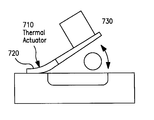
- Two specific subexamples directed to specific types of CMOS microactuators include a thermal actuator and a parallel plate actuator.
- a CMOS thermal actuator includes a cantilever beam 710 with materials of very different thermal expansion coefficients.
- a first material 720 of higher thermal expansion coefficient will shrink when the temperature is reduced, and deflect the cantilever beam 710 upward, if the left edge of a second material 730 (of lower expansion coefficient) is prevented from sliding to the left by a structure (not shown).
- a parallel plate actuator can be realized by undercutting a CMOS multilayer structure 810 with selective etching.
- Parallel plate actuators are electrostatic force between two parallel plates to move one moveable plate towards the other fixed plate.
- a bias between an upper CMOS layer 820 and a bottom 830 of an etched cavity 840 a suspended CMOS plate 850 can be attracted downward.
- CMOS embodiment is two plates that form a wedge rather than a parallel structure (e.g., a > shape).
- a parallel structure e.g., a > shape.
- CMOS actuators include low cost, broad availability of CMOS process, and monolithic integration with CMOS drive electronics.
- Another example includes stress-induced electrostatic gap-closing actuators with bonded vertical micromirror.
- a stress can be used to generate an electric field using a piezoelectric structure.
- the torsion plate includes a micromachined plate that is mechanically hinged about a pivot axis to a substrate.
- Another example includes a torsion plate with a permalloy layer and bonded vertical micromirrors.
- Permalloy is a brand name for any of a class of alloys of high magnetic permeability containing from approximately 30 to approximately 90 percent, by weight, of nickel.
- the torsion plate can be displaced with a magnetic field.
- Another example includes a vertical mirrors on torsion plate configured to move with a push-pull electrostatic force.
- the torsion plate can be displaced with an electric field.
- an optomechanical matrix switch is composed of an array of free-space optical switches, an input fiber array, and an output fiber array. Such arrangement, however, has non-uniform optical insertion losses.
- the optical path length is different when each switching cell is activated (e.g., the optical path length of input # 1 to output # 1 is less than that of input # 1 to output # 8 ).
- the invention includes an optomechanical matrix switch architecture that will have uniform optical coupling loss, independent of which switch is activated.
- a series of input fibers 910 are coupled to a substrate 920 .
- An array of optomechanical switching cells 930 is arranged on the substrate 920 .
- a series of output fibers 940 are also connected to the substrate 920 .
- an input fiber 950 can be provided with a lens 960 .
- an output fiber 970 can be provided with a lens 980 .
- the micro electro mechanical systems optomechanical switch of the invention offers unique advantages for integrating the photodetector arrays on the switch chip for power monitoring. The cost of adding this function to the switch is much lower for the monolithic micro electro mechanical systems switches than for macro scale optomechanical switches.
- FIGS. 10A-10B illustrate two architectures of the micro electro mechanical systems optical switch with input/output power monitoring capabilities.
- a plurality of vertical beamsplitters 1040 can be employed to deflect part of the optical beams to an input photodetector array 1010 and an output photodetector array 1020 .
- the deflection in this embodiment is coplanar with a substrate 1050 .
- a plurality of 45° beamsplitters 1060 can be employed to reflect part of the optical beams out of the switch plane to the photodetector arrays 1070 above the micro electro mechanical systems optical switch chip 1080 .
- the deflection in this embodiment is perpendicular to a substrate 1090 .
- the beamsplitters should be almost transparent (e.g., 1% reflection) to reduce the optical insertion loss.
- the beamsplitters 1040 in FIG. 10 ( a ) could be monolithically fabricated with the micro electro mechanical systems chip using the surface-micromachining microhinge technique. It is also possible to mount high quality external beamsplitters on the chip.
- the beamsplitters 1060 in FIGS. 10B-10C could be fabricated monolithically, or attached to the packages of the photodetector arrays so that the beamsplitter/photodetectors could be simply dropped onto the micro electro mechanical systems switch chip.
- a photodetector array 1005 at the opposite end of the input fibers to monitor possible failure micro electro mechanical systems micromirrors.
- at least one of the micromirrors in each column will be turned on. Therefore, no photocurrent will be registered in the photodetector array 1005 .
- a suitable photo-detector device can be provided by a p-n junction, for example, In Ga As, or Silicon or GaAs.
- the size of the micro electro mechanical systems optical switch is limited by the maximum coupling distance between the input and the output fibers.
- fiber collimators are employed for both input and output fibers.
- the maximum coupling distance between the input and output collimators determines the maximum size of the switch. For example, if the maximum coupling distance is 2 cm, and the switch cell area is 1 mm ⁇ 1 mm, then the largest switch that can be realized is 10 ⁇ 10. To increase the dimension of the switch, it is therefore desirable to be able to extend the coupling distance without sacrificing the coupling efficiency.
- the invention includes integrating microlenses on the micro electro mechanical systems optomechanical switching cells 1110 . This will extend the coupling distance without sacrificing the coupling efficiency.
- the microlenses can be directly formed on the surface of the micromirror 1120 .
- FIG. 11C illustrates a schematic drawings of the micromirror 1120 with an integrated diffractive microlens 1130 .
- FIG. 11B illustrates a schematic drawing of the micromirror 1120 with an integrated refractive microlens 1140 .
- the microlenses function as relay lenses to extend the coupling distance while maintaining the same optical insertion loss. It is noted that the microlens for each micromirror should be different for uniform coupling efficiency.
- the diffractive and refractive microlenses 1130 and 1140 can be integrated with surface-micromachined micro electro mechanical systems structures.
- a refractive lens can be integrated on a micro electro mechanical systems flip up structure.
- the integrated microlens acts as a relay lens. As the beam is loosing collimation, these integrated microlenses bring the beam back into collimation (parallel beams once again).
- Refractive lenses can be made with grinding glass, or moulding glass, or putting a gradient index in a cylinder of glass (GRIN).
- Diffractive lenses can be made by moulding or etching indentations in a piece of glass or other material according to a computer generated set of masks.
- a plurality of microlenses 1210 can also be integrated in between two of a plurality of micro electro mechanical systems micromirrors 1220 to extend the coupling distance. This is equivalent to stitching smaller micro electro mechanical systems optical switches together to form a larger dimension switch while maintaining almost the same optical insertion loss.
- the collimated beam will diverge again after a certain distance. This is known as throw distance.
- the beam it is highly desirable for the beam to stay collimated (otherwise it will become bigger than the switch and clipping loss will occur). Having another lens to “help” it stay collimated is the main purpose of integrating the lens onto the mirror itself.
- the invention includes providing an optomechanical matrix switch 1310 with one or more wavelength division devices 1320 .
- the wavelength division devices 1320 can include wavelength division multiplexers and/or wavelength division demultiplexers.
- the wavelength-division-multiplexing (WDM) components can be integrated with the micro electro mechanical systems optical switch to form more functional WDM micro electro mechanical systems switches.
- FIG. 13 One particular embodiment of such device is shown in FIG. 13 .
- the embodiment depicted in FIG. 13 includes WDM components.
- a first WDM micromirror 1330 reflects wavelength ⁇ 1 only when the mirror is turned on
- a second WDM micromirror 1340 reflects ⁇ 2 only when the WDM mirror is turned on; etc.
- Such a device can perform selective WDM add-drop multiplexing as well as optical switching. It is more powerful than combining discrete optical switches and external WDM multiplexers and/or demultiplexers. This means that the switch can be combined with WDM multiplexers/demultiplexers to form wavelength-selective add/drop filters that are programmable. It is better than combining a separate switch and a separate WDM filter because the coupling loss is reduced (there is no need to couple into fiber and then expand the beam from the fiber again).
- Hermetic sealing is very important for the operation of micro electro mechanical systems actuators and to reduce in-use stiction. Conventional hermetic sealing is applied at the package level.
- the invention includes on-chip hermetic sealing.
- On-chip hermetic sealing is very attractive for optical micro electro mechanical systems devices. Since the micro electro mechanical systems optomechanical devices are accessed by optical beams, the micro electro mechanical systems optomechanical devices can actually be sealed before dicing the chip.
- an optomechanical matrix switch 1410 with on-chip hermetic sealing feature is depicted.
- a sealing structure 1420 e.g., a transparent cap
- a substrate 1430 is connected to an optomechanical matrix switch 1410 with on-chip hermetic sealing feature.
- the micro electro mechanical systems optomechanical matrix switches can be fabricated by connecting the mirrors to the actuators at a wafer scale. Then the constraining structure that holds the actuators can be released. Then the devices can be hermetically sealed with the transparent cap. After sealing, the wafer can be treated as integrated circuit (IC) wafers, and be diced.
- IC integrated circuit
- the input and output fibers can be integrated monolithically with the micro electro mechanical systems optical switching chip by etching V-grooves for aligning the fibers. This will totally eliminate the optical alignment step in packaging. However, some optical alignment may be necessary because of the non-perfect angle of the micromirrors.
- the invention includes a micro electro mechanical systems optomechanical matrix switch combined with fiber ribbons.
- fiber ribbons for the input and output fibers, the optical alignment is greatly simplified. Instead of aligning 2N individual fibers, there is only a need to align 2 fiber ribbons.
- the invention also includes combining a micro electro mechanical systems optomechanical matrix switch 1510 with output fibers 1520 and input fibers 1530 located in V-grooves provided on a fiber-package chip 1540 .
- a micro electro mechanical systems optomechanical matrix switch 1510 With output fibers 1520 and input fibers 1530 located in V-grooves provided on a fiber-package chip 1540 .
- the fiber ribbons By mounting the fiber ribbons on V-grooves on the same silicon (Si) substrate, all fibers are automatically aligned.
- Si silicon
- the micro electro mechanical systems chip can be perfectly aligned to the fiber-package chip.
- a fiber package chip 1610 includes a plurality of optical fibers 1620 and a cylindrical lens 1630 .
- a micro electro mechanical systems matrix switch chip 1640 includes a plurality of micro mirrors 1650 . Even with perfect design, the mirror angle might still deviate slightly from 90°. With two degrees of freedom in rotation, this non-ideal mirror angle can be corrected during the packaging step.
- the tilt control restores the mirror to perfect 90° angle, while the rotation and linear translations accurately position the micro electro mechanical systems chip. Perfect alignment is represented in FIG. 16 by arrowheads pointing in opposite directions on a single ray.
- FIG. 17 illustratively represents a number of 3-port and 4-port matrix switches capable of being realized using the MEMS switching cells of the present invention.
- an optomechanical matrix switch 1700 a which includes a first plurality of switching cells 1710 a and a second plurality of switching cells 1720 a mounted upon a substrate 1730 a.
- the matrix switch 1700 a includes first and second optical fiber input ports 1740 a and 1750 a in optical alignment with the first plurality of switching cells 1710 a and the second plurality of switching cells 1720 a, respectively.
- a corresponding first plurality optical fiber output ports 1760 a are in optical alignment with the first plurality of switching cells 1710 a and a corresponding second plurality of optical fiber output ports 1770 a are in optical alignment with the second plurality of switching cells 1720 a.
- input beams are switched from the optical fiber input port 1740 a to a desired one of the optical fiber output ports 1760 a by actuating the applicable one of the switching cells 1710 a.
- input beams are switched from the optical fiber input port 1750 a to a desired one of the optical fiber output ports 1770 a by actuating the applicable one of the switching cells 1720 a.
- input beams are switched from the optical fiber input port 1740 b to a desired one of the optical fiber output ports 1760 b by actuating the applicable one of the switching cells 1710 b.
- input beams are switched from the optical fiber input port 1750 b to a desired one of the optical fiber output ports 1770 b by actuating the applicable one of the switching cells 1720 b.
- the optomechanical matrix switch 1700 b also includes a third plurality of switching cells 1780 b and a fourth plurality of switching cells 1784 b mounted upon a substrate 1730 b.
- the matrix switch 1700 b includes third and fourth optical fiber input ports 1786 b and 1788 b in optical alignment with the third plurality of switching cells 1780 b and the fourth plurality of switching cells 1784 b, respectively.
- a corresponding third plurality optical fiber output ports 1790 b are in optical alignment with the third plurality of switching cells 1780 b and a corresponding fourth plurality of optical fiber output ports 17920 b are in optical alignment with the fourth plurality of switching cells 1784 b.
- input beams are switched from the optical fiber input port 1786 b to a desired one of the optical fiber output ports 1790 b by actuating the applicable one of the switching cells 1780 b.
- input beams are switched from the optical fiber input port 1788 b to a desired one of the optical fiber output ports 1792 b by actuating the applicable one of the switching cells 1784 b.
- FIG. 17 c depicts an optomechanical matrix switch 1700 c which includes a first plurality of switching cells 1710 c and a second plurality of switching cells 1720 c mounted upon a substrate 1730 c.
- the matrix switch 1700 c includes first plurality of optical fiber input ports 1740 c in optical alignment with the first plurality of switching cells 1710 c, and an optical fiber add port 1750 c in optical alignment with the second plurality of switching cells 1720 c.
- Each of the first plurality of optical switching cells 1710 c is also in optical alignment with an optical fiber drop port 1760 c.
- a plurality of optical fiber output ports 1770 c are in optical alignment with the second plurality of switching cells 1720 c.
- input beams are switched from a selected one of the optical fiber input ports 1740 c to the optical fiber drop port 1760 c by actuating the applicable one of the switching cells 1710 c.
- input beams are switched from the optical fiber add port 1750 c to a desired one of the optical fiber output ports 1770 c by actuating the applicable one of the switching cells 1720 c.
- input beams from the input ports 1740 c may be allowed to pass to corresponding ones of the output ports 1770 c in optical alignment therewith by refraining from actuating the applicable switching cells 1710 c.
- an optomechanical matrix switch 1700 d including a first plurality of switching cells 1710 d and a second plurality of switching cells 1720 d mounted upon a substrate 1730 d.
- the matrix switch 1700 d includes a first plurality of optical fiber input ports 1740 d in optical alignment with the first plurality of switching cells 1710 d, and a first optical fiber add port 1750 d in optical alignment with the second plurality of switching cells 1720 d.
- Each of the first plurality of optical switching cells 1710 d is also in optical alignment with a first optical fiber drop port 1760 d.
- a first plurality of optical fiber output ports 1770 d are in optical alignment with the second plurality of switching cells 1720 d.
- input beams are switched from a selected one of the optical fiber input ports 1740 d to the optical fiber drop port 1760 d by actuating the applicable one of the switching cells 1710 d.
- input beams are switched from the optical fiber add port 1750 d to a desired one of the optical fiber output ports 1770 d by actuating the applicable one of the switching cells 1720 d.
- input beams from the input ports 1740 d may be allowed to pass to corresponding ones of the output ports 1770 d in optical alignment therewith by refraining from actuating the applicable switching cells 1710 d.
- the optomechanical matrix switch 1700 d further includes a third plurality of switching cells 1780 d and a fourth plurality of switching cells 1784 d mounted upon the substrate 1730 d.
- the matrix switch 1700 d also includes a third plurality of optical fiber input ports 1786 d in optical alignment with the third plurality of switching cells 1780 d, and a second optical fiber add port 1788 d in optical alignment with the second plurality of switching cells 1784 d.
- Each of the third plurality of optical switching cells 1780 d is also in optical alignment with a second optical fiber drop port 1790 d.
- a second plurality of optical fiber output ports 1792 d are in optical alignment with the second plurality of switching cells 1784 d.
- input beams are switched from a selected one of the optical fiber input ports 1786 d to the optical fiber drop port 1790 d by actuating the applicable one of the switching cells 1780 d.
- input beams are switched from the optical fiber add port 1788 d to a desired one of the optical fiber output ports 1792 d by actuating the applicable one of the switching cells 1784 d.
- input beams from the input ports 1786 d may be allowed to pass to corresponding ones of the output ports 1792 d in optical alignment therewith by refraining from actuating the applicable switching cells 1780 d.
- an optomechanical matrix switch 1700 e including a first plurality of switching cells 1710 e and a second plurality of switching cells 1720 e mounted upon a substrate 1730 e.
- the matrix switch 1700 e includes a plurality of optical fiber input ports 1740 e in optical alignment with the first plurality of switching cells 1710 e, and a plurality optical fiber add ports 1750 e in optical alignment with the second plurality of switching cells 1720 e.
- Each of the plurality of optical switching cells 1710 e is also in optical alignment with a corresponding one of a plurality of optical fiber drop ports 1760 e.
- a first plurality of optical fiber output ports 1770 e are in optical alignment with the second plurality of switching cells 1720 e.
- input beams are switched from a selected one of the optical fiber input ports 1740 e to a corresponding one of the optical fiber drop ports 1760 e by actuating the applicable one of the switching cells 1710 e.
- input beams are switched from a selected one of the optical fiber add ports 1750 e to a desired one of the optical fiber output ports 1770 e by actuating the applicable one of the switching cells 1720 e.
- input beams from the input ports 1740 e may be allowed to pass to corresponding ones of the output ports 1770 e in optical alignment therewith by refraining from actuating the applicable switching cells 1710 e.
- FIG. 17 f provides an illustrative representation of an optomechanical matrix switch 1700 f including a first plurality of switching cells 1710 f and a second plurality of switching cells 1720 f mounted upon a substrate 1730 f.
- the matrix switch 1700 f includes a first plurality of optical fiber input ports 1740 f in optical alignment with the first plurality of switching cells 1710 f, and a first plurality optical fiber add ports 1750 f in optical alignment with the second plurality of switching cells 1720 f.
- Each of the plurality of optical switching cells 1710 f is also in optical alignment with a corresponding one of a first plurality of optical fiber drop ports 1760 f.
- a first plurality of optical fiber output ports 1770 f are in optical alignment with the second plurality of switching cells 1720 f.
- input beams are switched from a selected one of the optical fiber input ports 1740 f to a corresponding one of the optical fiber drop ports 1760 f by actuating the applicable one of the switching cells 1710 f.
- input beams are switched from a selected one of the optical fiber add ports 1750 f to a desired one of the optical fiber output ports 1770 f by actuating the applicable one of the switching cells 1720 f.
- input beams from the input ports 1740 f may be allowed to pass to corresponding ones of the output ports 1770 f in optical alignment therewith by refraining from actuating the applicable switching cells 1710 f.
- the optomechanical matrix switch 1700 f further includes a third plurality of switching cells 1780 f and a fourth plurality of switching cells 1784 f mounted upon the substrate 1730 f.
- the matrix switch 1700 f includes a second plurality of optical fiber input ports 1786 f in optical alignment with the third plurality of switching cells 1780 f, and a second plurality optical fiber add ports 1788 f in optical alignment with the fourth plurality of switching cells 1784 f.
- Each of the plurality of optical switching cells 1780 f is also in optical alignment with a corresponding one of a second plurality of optical fiber drop ports 1790 f.
- a second plurality of optical fiber output ports 1792 f are in optical alignment with the fourth plurality of switching cells 1784 f.
- input beams are switched from a selected one of the optical fiber input ports 1786 f to a corresponding one of the optical fiber drop ports 1790 f by actuating the applicable one of the switching cells 1780 f.
- input beams are switched from a selected one of the optical fiber add ports 1788 f to a desired one of the optical fiber output ports 1792 f by actuating the applicable one of the switching cells 1784 f.
- input beams from the input ports 1786 f may be allowed to pass to corresponding ones of the output ports 1792 f in optical alignment therewith by refraining from actuating the applicable switching cells 1780 f.
- an optomechanical matrix switch 1700 g including a first plurality of switching cells 1710 g and a second plurality of switching cells 1720 g mounted upon a substrate 1730 g.
- the matrix switch 1700 g includes a plurality of optical fiber input ports 1740 g in optical alignment with the first plurality of switching cells 1710 g, and a plurality optical fiber add ports 1750 g in optical alignment with the second plurality of switching cells 1720 g.
- Each of the plurality of optical switching cells 171 0 g is also in optical alignment with a corresponding one of a plurality of optical fiber drop ports 1760 g.
- a first plurality of optical fiber output ports 1770 g are in optical alignment with the second plurality of switching cells 1720 g.
- the add ports 1750 g are arranged along a border of the matrix switch 1700 g opposite to a border along which are arranged the drop ports 1760 g.
- input beams are switched from a selected one of the optical fiber input ports 1740 g to a corresponding one of the optical fiber drop ports 1760 g by actuating the applicable one of the switching cells 1710 g.
- input beams are switched from a selected one of the optical fiber add ports 1750 g to a desired one of the optical fiber output ports 1770 g by actuating the applicable one of the switching cells 1720 g.
- input beams from the input ports 1740 g may be allowed to pass to corresponding ones of the output ports 1770 g in optical alignment therewith by refraining from actuating the applicable switching cells 1710 g.
- FIG. 17 h depicts an optomechanical matrix switch 1700 h which includes a plurality of switching cells 1710 h mounted upon a substrate 1730 h.
- the matrix switch 1700 h includes a plurality of optical fiber input ports 1740 h in optical alignment with the plurality of switching cells 1710 h.
- Each of the plurality of optical switching cells 1710 h is also in optical alignment with a corresponding one of a plurality of first optical fiber output ports 1760 h, and is interposed between one of the input ports 1740 h and a corresponding one of a plurality of second optical fiber output ports 1760 h.
- input beams are switched from a selected one of the optical fiber input ports 1740 h to a corresponding one of the first optical fiber output ports 1760 h by actuating the applicable one of the switching cells 1710 h.
- input beams from the input ports 1740 h may be allowed to pass to corresponding ones of the second optical fiber output ports 1770 h in optical alignment therewith by refraining from actuating the applicable switching cells 1710 h.
- the invention can be applied to network restoration, reconfiguration, and dynamic bandwidth allocation.
- the invention can be embodied in an optical crossbar switch (N ⁇ M matrix switch) which is a general purpose switch that is very useful for reconfiguring large telecommunication fiber optic networks, restoration of services and dynamic allocation of bandwidth.
- N ⁇ M matrix switch is a general purpose switch that is very useful for reconfiguring large telecommunication fiber optic networks, restoration of services and dynamic allocation of bandwidth.
- An optomechanical switch made with micro electro mechanical systems technology offers significant advantages over conventional optomechanical switches for realizing optical crossbar switches. Since the surface area (footprint) of a micro electro mechanical systems fabricated switching cell is very small (e.g., from a few hundred micrometers to a few millimeters), an entire N ⁇ M switching matrix can be monolithically integrated on a single substrate (e.g., a single silicon integrated circuit chip). This significantly reduces the packaging cost of the switch. It also enables the entire switch to be hermetically packaged, which is a very important factor for the switch to satisfy the temperature and humidity requirements such as those in the Bellcore standard.
- the switching time can also be reduced because of their higher resonant frequency.
- the resonant frequency is proportional to the square root of the ratio of spring constant and mass.
- Switch cells fabricated in accordance with the invention can be much smaller (e.g., 10-100 smaller) physically than bulk mechanical switches. Consequently, switch cells fabricated in accordance with the invention can have smaller mass and, therefore, a higher resonant frequency.
- the higher resonant frequency is directly proportional to the speed of switching of the device.
- an optomechanical switch made with micro electro mechanical systems technology can be more rugged than the macro-scale switches because the inertial forces are much smaller in the micro-scale switches.
- the individual components need not be formed in the disclosed shapes, or assembled in the disclosed configuration, but could be provided in virtually any shape, and assembled in virtually any configuration. Further, the individual components need not be fabricated from the disclosed materials, but could be fabricated from virtually any suitable materials. Further, although the N ⁇ M matrices are described herein as physically separate modules, it is understood that the matrices may be integrated into the apparatus with which they are associated. Furthermore, all the disclosed elements and feature of each disclosed embodiment can be combined with, or substituted for, the disclosed elements and features of every other disclosed embodiment except where such elements or features are mutually exclusive.
Abstract
Description
Claims (18)
Priority Applications (4)
| Application Number | Priority Date | Filing Date | Title |
|---|---|---|---|
| US09/483,269 US6445840B1 (en) | 1999-05-28 | 2000-01-13 | Micromachined optical switching devices |
| AU60471/00A AU6047100A (en) | 1999-05-28 | 2000-05-26 | Micromachined optical switching devices |
| PCT/US2000/014701 WO2000073841A1 (en) | 1999-05-28 | 2000-05-26 | Micromachined optical switching devices |
| EP00946767A EP1181612A1 (en) | 1999-05-28 | 2000-05-26 | Micromachined optical switching devices |
Applications Claiming Priority (2)
| Application Number | Priority Date | Filing Date | Title |
|---|---|---|---|
| US13643899P | 1999-05-28 | 1999-05-28 | |
| US09/483,269 US6445840B1 (en) | 1999-05-28 | 2000-01-13 | Micromachined optical switching devices |
Publications (1)
| Publication Number | Publication Date |
|---|---|
| US6445840B1 true US6445840B1 (en) | 2002-09-03 |
Family
ID=26834298
Family Applications (1)
| Application Number | Title | Priority Date | Filing Date |
|---|---|---|---|
| US09/483,269 Expired - Fee Related US6445840B1 (en) | 1999-05-28 | 2000-01-13 | Micromachined optical switching devices |
Country Status (4)
| Country | Link |
|---|---|
| US (1) | US6445840B1 (en) |
| EP (1) | EP1181612A1 (en) |
| AU (1) | AU6047100A (en) |
| WO (1) | WO2000073841A1 (en) |
Cited By (19)
| Publication number | Priority date | Publication date | Assignee | Title |
|---|---|---|---|---|
| US6587610B2 (en) * | 2001-01-26 | 2003-07-01 | Jds Uniphase Inc. | Segmented optical switch |
| US6639713B2 (en) * | 2000-04-25 | 2003-10-28 | Umachines, Inc. | Silicon micromachined optical device |
| US6709886B2 (en) | 2000-04-25 | 2004-03-23 | Umachines, Inc. | Method of fabricating micromachined devices |
| US20040213503A1 (en) * | 2002-09-19 | 2004-10-28 | Cham Kit M. | Highly parallel optical communication system with intracard and intercard communications |
| US20050018955A1 (en) * | 2001-12-26 | 2005-01-27 | Nikon Corporation | Light-beam switching/adjusting apparatus and manufacturing method thereof |
| US6873756B2 (en) * | 2001-09-07 | 2005-03-29 | Analog Devices, Inc. | Tiling of optical MEMS devices |
| US20050069245A1 (en) * | 2003-09-30 | 2005-03-31 | Mitchell Thomas A. | Compact optical switches |
| US20050163417A1 (en) * | 2002-01-18 | 2005-07-28 | Teem Photonics | Optical switch with a micro-mirror and method for production thereof |
| US20050286110A1 (en) * | 2004-06-25 | 2005-12-29 | Industrial Technology Research Institute | MEMS optical switch with self-assembly structure |
| US20060049826A1 (en) * | 2001-03-01 | 2006-03-09 | Onix Microsystems | Optical cross-connect system |
| US20060098982A1 (en) * | 2000-12-19 | 2006-05-11 | Schofield Bruce A | System and apparatus for dropping and adding optical data streams in an optical communication network |
| US20090067781A1 (en) * | 2007-09-11 | 2009-03-12 | National Taiwan University | Optical switch |
| US7623789B2 (en) * | 2001-04-11 | 2009-11-24 | Transmode Holding Ab | Low loss WDM add drop node |
| US7785098B1 (en) | 2001-06-05 | 2010-08-31 | Mikro Systems, Inc. | Systems for large area micro mechanical systems |
| EP2559534A2 (en) | 2008-09-26 | 2013-02-20 | Mikro Systems Inc. | Systems, devices, and/or methods for manufacturing castings |
| US20130170791A1 (en) * | 2010-09-07 | 2013-07-04 | Ntt Electronics Corporation | Optical module |
| US8540913B2 (en) | 2001-06-05 | 2013-09-24 | Mikro Systems, Inc. | Methods for manufacturing three-dimensional devices and devices created thereby |
| US8813824B2 (en) | 2011-12-06 | 2014-08-26 | Mikro Systems, Inc. | Systems, devices, and/or methods for producing holes |
| US10317626B2 (en) | 2017-06-15 | 2019-06-11 | Google Llc | Inner and outer collimator elements for an optical circuit switch |
Families Citing this family (3)
| Publication number | Priority date | Publication date | Assignee | Title |
|---|---|---|---|---|
| US6366715B1 (en) * | 2000-03-03 | 2002-04-02 | Agilent Technologies, Inc. | Free space optical switch with lenses for re-collimating the light |
| US6901180B2 (en) | 2001-01-24 | 2005-05-31 | Adc Telecommunications, Inc. | MEMS optical switch on a single chip and method |
| EP2896630B1 (en) | 2007-01-30 | 2020-12-23 | Epivax, Inc. | Regulatory t cell epitopes, compositions and uses thereof |
Citations (94)
| Publication number | Priority date | Publication date | Assignee | Title |
|---|---|---|---|---|
| US3430057A (en) | 1965-06-22 | 1969-02-25 | Schneider Co Optische Werke | Episcopic scanning head having smaller optical fibers interleaved in interstices formed by contiguous larger fibers |
| US3622792A (en) | 1969-12-29 | 1971-11-23 | Bell Telephone Labor Inc | Optical switching system |
| US3990780A (en) | 1975-08-22 | 1976-11-09 | Gte Laboratories Incorporated | Optical switch |
| US4208094A (en) | 1978-10-02 | 1980-06-17 | Bell Telephone Laboratories, Incorporated | Optical switch |
| US4303302A (en) | 1979-10-30 | 1981-12-01 | Gte Laboratories Incorporated | Piezoelectric optical switch |
| US4317611A (en) | 1980-05-19 | 1982-03-02 | International Business Machines Corporation | Optical ray deflection apparatus |
| US4580873A (en) * | 1983-12-30 | 1986-04-08 | At&T Bell Laboratories | Optical matrix switch |
| US4626066A (en) | 1983-12-30 | 1986-12-02 | At&T Bell Laboratories | Optical coupling device utilizing a mirror and cantilevered arm |
| US4630883A (en) | 1983-03-21 | 1986-12-23 | The United States Of America As Represented By The Secretary Of The Navy | Optical waveguide apparatus and method for manufacturing |
| US4740050A (en) | 1982-07-06 | 1988-04-26 | Honeywell Inc. | Optical fail safe device |
| US4762382A (en) | 1987-06-29 | 1988-08-09 | Honeywell Inc. | Optical interconnect circuit for GaAs optoelectronics and Si VLSI/VHSIC |
| US4850697A (en) | 1988-03-16 | 1989-07-25 | Dynatech Electro-Optics Corporation | Resonant piezoelectric chopper for infrared radiation |
| JPH01238605A (en) | 1988-03-18 | 1989-09-22 | Matsushita Electric Ind Co Ltd | Optical switch |
| US4932745A (en) | 1989-07-25 | 1990-06-12 | At&T Bell Laboratories | Radiation switching arrangement with moving deflecting element |
| US4989941A (en) | 1988-03-18 | 1991-02-05 | The United States Of America As Represented By The Secretary Of The Air Force | Normal incidence optical switches using ferroelectric liquid crystals |
| US5037173A (en) | 1989-11-22 | 1991-08-06 | Texas Instruments Incorporated | Optical interconnection network |
| US5042889A (en) | 1990-04-09 | 1991-08-27 | At&T Bell Laboratories | Magnetic activation mechanism for an optical switch |
| US5052777A (en) | 1988-04-27 | 1991-10-01 | Sportsoft Systems, Inc. | Graphics display using bimorphs |
| US5097229A (en) | 1989-01-12 | 1992-03-17 | Uniphase Corporation | Modulator - demodulator transformer coupled d.c. to one mhz information channel |
| EP0510629A1 (en) | 1991-04-26 | 1992-10-28 | Texas Instruments Incorporated | Deformable mirror shutter device |
| US5168535A (en) | 1985-12-24 | 1992-12-01 | Herzel Laor | Integrated optic switch |
| US5199088A (en) | 1991-12-31 | 1993-03-30 | Texas Instruments Incorporated | Fiber optic switch with spatial light modulator device |
| US5208880A (en) | 1992-04-30 | 1993-05-04 | General Electric Company | Microdynamical fiber-optic switch and method of switching using same |
| US5255332A (en) | 1992-07-16 | 1993-10-19 | Sdl, Inc. | NxN Optical crossbar switch matrix |
| US5278515A (en) | 1992-12-24 | 1994-01-11 | Uniphase Corporation | High bandwidth information channel with optocoupling isolation |
| US5311410A (en) | 1992-10-29 | 1994-05-10 | Hughes Aircraft Company | Distributed lighting system with fiber optic controls |
| US5317659A (en) | 1993-02-09 | 1994-05-31 | Dicon Fiberoptics | Conical fiberoptic switch |
| US5351330A (en) | 1993-04-08 | 1994-09-27 | Uniphase Corporation | Laser diode-lens alignment |
| US5375033A (en) | 1992-04-14 | 1994-12-20 | Cornell Research Foundation, Inc. | Multi-dimensional precision micro-actuator |
| US5410371A (en) | 1993-06-07 | 1995-04-25 | The United States Of America As Represented By The Administrator Of The National Aeronautics And Space Administration | Display system employing acoustro-optic tunable filter |
| US5420946A (en) | 1993-03-09 | 1995-05-30 | Tsai; Jian-Hung | Multiple channel optical coupling switch |
| US5428218A (en) | 1993-09-30 | 1995-06-27 | The United States Of America As Represented By The Secretary Of The Air Force | Variable time-delay system for broadband phased array and other transversal filtering applications |
| US5436986A (en) | 1993-03-09 | 1995-07-25 | Tsai; Jian-Hung | Apparatus for switching optical signals among optical fibers and method |
| US5444801A (en) | 1994-05-27 | 1995-08-22 | Laughlin; Richard H. | Apparatus for switching optical signals and method of operation |
| US5524153A (en) | 1995-02-10 | 1996-06-04 | Astarte Fiber Networks, Inc. | Optical fiber switching system and method using same |
| US5522796A (en) | 1990-01-26 | 1996-06-04 | C.R. Bard, Inc. | Metering gauge trumpet valve |
| DE19500214A1 (en) | 1995-01-05 | 1996-07-11 | Lightway Technology Gmbh I Gr | Switching between optical signal lines |
| US5555327A (en) | 1995-06-07 | 1996-09-10 | Laughlin; Richard H. | Frustrated total internal reflection device |
| US5572014A (en) | 1994-07-14 | 1996-11-05 | The Regents Of The University Of California | Highly efficient, ultrafast optical-to-electrical converter and method of operating the same |
| US5581643A (en) | 1994-12-08 | 1996-12-03 | Northern Telecom Limited | Optical waveguide cross-point switch |
| US5621829A (en) | 1996-04-02 | 1997-04-15 | Lucent Technologies Inc. | Fiber optic switching device and method using free space scanning |
| US5646928A (en) | 1995-06-22 | 1997-07-08 | The Regents Of The University Of California | Free-space integrated micro-pickup head for optical data storage and a micro-optical bench |
| US5651023A (en) | 1995-05-13 | 1997-07-22 | Uniphase Lasers Limited | Monolithic laser |
| WO1998009289A1 (en) | 1996-08-27 | 1998-03-05 | Quinta Corporation | Optical head using micro-machined elements |
| DE19644918A1 (en) | 1996-10-29 | 1998-04-30 | Cms Mikrosysteme Gmbh Chemnitz | Micromechanical optical switch |
| US5774604A (en) | 1996-10-23 | 1998-06-30 | Texas Instruments Incorporated | Using an asymmetric element to create a 1XN optical switch |
| US5786925A (en) | 1993-11-01 | 1998-07-28 | Lucent Technologies Inc. | Method and composition for arbitrary angle mirrors in substrates for use in hybrid optical systems |
| US5835212A (en) | 1996-10-18 | 1998-11-10 | Uniphase Telecommunications Products, Inc. | Variable chirp optical modulator using single modulation source |
| US5841917A (en) * | 1997-01-31 | 1998-11-24 | Hewlett-Packard Company | Optical cross-connect switch using a pin grid actuator |
| EP0880040A2 (en) | 1997-05-15 | 1998-11-25 | Lucent Technologies Inc. | Micro machined optical switch |
| US5867297A (en) | 1997-02-07 | 1999-02-02 | The Regents Of The University Of California | Apparatus and method for optical scanning with an oscillatory microelectromechanical system |
| US5878177A (en) | 1997-03-31 | 1999-03-02 | At&T Corp. | Layered switch architectures for high-capacity optical transport networks |
| EP0902538A2 (en) | 1997-09-10 | 1999-03-17 | Lucent Technologies Inc. | Article comprising a light-actuated micromechanical photonic switch |
| EP0903607A2 (en) | 1997-08-15 | 1999-03-24 | Lucent Technologies Inc. | Freespace optical bypass-exchange switch |
| US5903687A (en) * | 1997-05-02 | 1999-05-11 | Neos Technologies, Inc. | M input port by N output port optical switching system |
| EP0921702A2 (en) | 1997-12-05 | 1999-06-09 | Lucent Technologies Inc. | Free-space optical signal switch arrangement |
| US5933269A (en) | 1997-08-22 | 1999-08-03 | Lucent Technologies Inc. | Common-lens reflective magneto-optical switch |
| US5945898A (en) | 1996-05-31 | 1999-08-31 | The Regents Of The University Of California | Magnetic microactuator |
| US5960131A (en) * | 1998-02-04 | 1999-09-28 | Hewlett-Packard Company | Switching element having an expanding waveguide core |
| US5960132A (en) * | 1997-09-09 | 1999-09-28 | At&T Corp. | Fiber-optic free-space micromachined matrix switches |
| US5995688A (en) * | 1998-06-01 | 1999-11-30 | Lucent Technologies, Inc. | Micro-opto-electromechanical devices and method therefor |
| US6031947A (en) | 1998-06-05 | 2000-02-29 | Laor; Herzel | 1×N optical switch |
| US6031946A (en) | 1998-04-16 | 2000-02-29 | Lucent Technologies Inc. | Moving mirror switch |
| US6108466A (en) | 1998-09-17 | 2000-08-22 | Lucent Technologies | Micro-machined optical switch with tapered ends |
| EP1033601A1 (en) | 1999-03-04 | 2000-09-06 | Japan Aviation Electronics Industry, Limited | Optical switch and method of making the same |
| US6125218A (en) | 1998-03-19 | 2000-09-26 | Humphrey; Ashley C. | Fiber optic pressure sensitive optical switch and apparatus incorporating same |
| US6137103A (en) | 1998-07-31 | 2000-10-24 | Lucent Technologies | Opto-mechanical components |
| US6137105A (en) | 1998-06-02 | 2000-10-24 | Science Applications International Corporation | Multiple parallel source scanning device |
| US6137926A (en) | 1996-08-12 | 2000-10-24 | Maynard; Ronald S. | Hybrid optical multi-axis beam steering apparatus |
| US6144781A (en) * | 1997-12-31 | 2000-11-07 | At&T Corp. | Symmetrical optical matrix crossconnect apparatus and method therefor |
| US6154585A (en) | 1999-06-17 | 2000-11-28 | Jds Fitel Inc. | 11/2×2 optical switch |
| US6154586A (en) | 1998-12-24 | 2000-11-28 | Jds Fitel Inc. | Optical switch mechanism |
| US6157026A (en) | 1998-11-19 | 2000-12-05 | Maxtec International Corporation | Optical switch of the multiple push button type for producing a plurality of control signals |
| US6160928A (en) | 1999-04-16 | 2000-12-12 | Agilent Technologies, Inc. | Fault tolerant optical switch |
| US6169827B1 (en) | 1999-09-03 | 2001-01-02 | Honeywell International Inc. | Micro-optic switch with lithographically fabricated polymer alignment features for the positioning of switch components and optical fibers |
| US6173105B1 (en) | 1998-11-20 | 2001-01-09 | Lucent Technologies | Optical attenuator |
| EP1067421A2 (en) | 1999-07-07 | 2001-01-10 | Agilent Technologies Inc., A Delaware Corporation | An optical switching device and method utilizing fluid pressure control to improve switching characteristics |
| EP1076254A2 (en) | 1999-08-11 | 2001-02-14 | Agilent Technologies Inc. (a Delaware Corporation) | Loss equalization in a multistage optical switch |
| US6195478B1 (en) | 1998-02-04 | 2001-02-27 | Agilent Technologies, Inc. | Planar lightwave circuit-based optical switches using micromirrors in trenches |
| US6205267B1 (en) | 1998-11-20 | 2001-03-20 | Lucent Technologies | Optical switch |
| US6208777B1 (en) | 1999-10-12 | 2001-03-27 | Primawave Photonics, Inc. | Actuator assembly for optical switches |
| US6215222B1 (en) | 1999-03-30 | 2001-04-10 | Agilent Technologies, Inc. | Optical cross-connect switch using electrostatic surface actuators |
| US6215919B1 (en) | 1999-06-15 | 2001-04-10 | Oplink Communications, Inc. | Mechanical optical switching device |
| US6218762B1 (en) | 1999-05-03 | 2001-04-17 | Mcnc | Multi-dimensional scalable displacement enabled microelectromechanical actuator structures and arrays |
| US6219472B1 (en) | 1997-02-17 | 2001-04-17 | Hitachi, Ltd. | Optical switch, method of manufacturing same, and optical communication equipment using the same |
| US6229640B1 (en) | 1999-08-11 | 2001-05-08 | Adc Telecommunications, Inc. | Microelectromechanical optical switch and method of manufacture thereof |
| EP1099971A2 (en) | 1999-11-10 | 2001-05-16 | Lucent Technologies Inc. | Microelectromechanical optical isolators |
| EP1099966A2 (en) | 1999-11-09 | 2001-05-16 | Texas Instruments Incorporated | Micromirror optical switch |
| US6236491B1 (en) | 1999-05-27 | 2001-05-22 | Mcnc | Micromachined electrostatic actuator with air gap |
| EP1102104A2 (en) | 1999-11-17 | 2001-05-23 | Lucent Technologies Inc. | Optical switch |
| EP1103835A1 (en) | 1999-09-03 | 2001-05-30 | Lucent Technologies Inc. | Micro-electro-mechanical optical device |
| US6243507B1 (en) | 1999-06-07 | 2001-06-05 | At&T Corp. | Connection-verification in optical MEMS crossconnects via mirror-dither |
| EP1104746A1 (en) | 1999-09-03 | 2001-06-06 | Lucent Technologies Inc. | Micro-electro-mechanical optical device |
| US6246504B1 (en) | 1999-06-30 | 2001-06-12 | The Regents Of The University Of Caifornia | Apparatus and method for optical raster-scanning in a micromechanical system |
-
2000
- 2000-01-13 US US09/483,269 patent/US6445840B1/en not_active Expired - Fee Related
- 2000-05-26 WO PCT/US2000/014701 patent/WO2000073841A1/en not_active Application Discontinuation
- 2000-05-26 EP EP00946767A patent/EP1181612A1/en not_active Withdrawn
- 2000-05-26 AU AU60471/00A patent/AU6047100A/en not_active Abandoned
Patent Citations (100)
| Publication number | Priority date | Publication date | Assignee | Title |
|---|---|---|---|---|
| US3430057A (en) | 1965-06-22 | 1969-02-25 | Schneider Co Optische Werke | Episcopic scanning head having smaller optical fibers interleaved in interstices formed by contiguous larger fibers |
| US3622792A (en) | 1969-12-29 | 1971-11-23 | Bell Telephone Labor Inc | Optical switching system |
| US3990780A (en) | 1975-08-22 | 1976-11-09 | Gte Laboratories Incorporated | Optical switch |
| US4208094A (en) | 1978-10-02 | 1980-06-17 | Bell Telephone Laboratories, Incorporated | Optical switch |
| US4303302A (en) | 1979-10-30 | 1981-12-01 | Gte Laboratories Incorporated | Piezoelectric optical switch |
| US4317611A (en) | 1980-05-19 | 1982-03-02 | International Business Machines Corporation | Optical ray deflection apparatus |
| US4740050A (en) | 1982-07-06 | 1988-04-26 | Honeywell Inc. | Optical fail safe device |
| US4630883A (en) | 1983-03-21 | 1986-12-23 | The United States Of America As Represented By The Secretary Of The Navy | Optical waveguide apparatus and method for manufacturing |
| US4626066A (en) | 1983-12-30 | 1986-12-02 | At&T Bell Laboratories | Optical coupling device utilizing a mirror and cantilevered arm |
| US4580873A (en) * | 1983-12-30 | 1986-04-08 | At&T Bell Laboratories | Optical matrix switch |
| US5168535A (en) | 1985-12-24 | 1992-12-01 | Herzel Laor | Integrated optic switch |
| US4762382A (en) | 1987-06-29 | 1988-08-09 | Honeywell Inc. | Optical interconnect circuit for GaAs optoelectronics and Si VLSI/VHSIC |
| US4850697A (en) | 1988-03-16 | 1989-07-25 | Dynatech Electro-Optics Corporation | Resonant piezoelectric chopper for infrared radiation |
| US4989941A (en) | 1988-03-18 | 1991-02-05 | The United States Of America As Represented By The Secretary Of The Air Force | Normal incidence optical switches using ferroelectric liquid crystals |
| JPH01238605A (en) | 1988-03-18 | 1989-09-22 | Matsushita Electric Ind Co Ltd | Optical switch |
| US5052777A (en) | 1988-04-27 | 1991-10-01 | Sportsoft Systems, Inc. | Graphics display using bimorphs |
| US5097229A (en) | 1989-01-12 | 1992-03-17 | Uniphase Corporation | Modulator - demodulator transformer coupled d.c. to one mhz information channel |
| US4932745A (en) | 1989-07-25 | 1990-06-12 | At&T Bell Laboratories | Radiation switching arrangement with moving deflecting element |
| US5037173A (en) | 1989-11-22 | 1991-08-06 | Texas Instruments Incorporated | Optical interconnection network |
| US5522796A (en) | 1990-01-26 | 1996-06-04 | C.R. Bard, Inc. | Metering gauge trumpet valve |
| US5042889A (en) | 1990-04-09 | 1991-08-27 | At&T Bell Laboratories | Magnetic activation mechanism for an optical switch |
| EP0510629A1 (en) | 1991-04-26 | 1992-10-28 | Texas Instruments Incorporated | Deformable mirror shutter device |
| US5199088A (en) | 1991-12-31 | 1993-03-30 | Texas Instruments Incorporated | Fiber optic switch with spatial light modulator device |
| EP0550017A2 (en) | 1991-12-31 | 1993-07-07 | Texas Instruments Incorporated | Fiber optic switch with spatial light modulator device |
| US5375033A (en) | 1992-04-14 | 1994-12-20 | Cornell Research Foundation, Inc. | Multi-dimensional precision micro-actuator |
| US5208880A (en) | 1992-04-30 | 1993-05-04 | General Electric Company | Microdynamical fiber-optic switch and method of switching using same |
| US5255332A (en) | 1992-07-16 | 1993-10-19 | Sdl, Inc. | NxN Optical crossbar switch matrix |
| US5311410A (en) | 1992-10-29 | 1994-05-10 | Hughes Aircraft Company | Distributed lighting system with fiber optic controls |
| US5278515A (en) | 1992-12-24 | 1994-01-11 | Uniphase Corporation | High bandwidth information channel with optocoupling isolation |
| US5317659A (en) | 1993-02-09 | 1994-05-31 | Dicon Fiberoptics | Conical fiberoptic switch |
| US5420946A (en) | 1993-03-09 | 1995-05-30 | Tsai; Jian-Hung | Multiple channel optical coupling switch |
| US5436986A (en) | 1993-03-09 | 1995-07-25 | Tsai; Jian-Hung | Apparatus for switching optical signals among optical fibers and method |
| US5351330A (en) | 1993-04-08 | 1994-09-27 | Uniphase Corporation | Laser diode-lens alignment |
| US5410371A (en) | 1993-06-07 | 1995-04-25 | The United States Of America As Represented By The Administrator Of The National Aeronautics And Space Administration | Display system employing acoustro-optic tunable filter |
| US5428218A (en) | 1993-09-30 | 1995-06-27 | The United States Of America As Represented By The Secretary Of The Air Force | Variable time-delay system for broadband phased array and other transversal filtering applications |
| US5786925A (en) | 1993-11-01 | 1998-07-28 | Lucent Technologies Inc. | Method and composition for arbitrary angle mirrors in substrates for use in hybrid optical systems |
| US5444801A (en) | 1994-05-27 | 1995-08-22 | Laughlin; Richard H. | Apparatus for switching optical signals and method of operation |
| US5572014A (en) | 1994-07-14 | 1996-11-05 | The Regents Of The University Of California | Highly efficient, ultrafast optical-to-electrical converter and method of operating the same |
| US5581643A (en) | 1994-12-08 | 1996-12-03 | Northern Telecom Limited | Optical waveguide cross-point switch |
| DE19500214A1 (en) | 1995-01-05 | 1996-07-11 | Lightway Technology Gmbh I Gr | Switching between optical signal lines |
| US5524153A (en) | 1995-02-10 | 1996-06-04 | Astarte Fiber Networks, Inc. | Optical fiber switching system and method using same |
| US5651023A (en) | 1995-05-13 | 1997-07-22 | Uniphase Lasers Limited | Monolithic laser |
| US5555327A (en) | 1995-06-07 | 1996-09-10 | Laughlin; Richard H. | Frustrated total internal reflection device |
| US5646928A (en) | 1995-06-22 | 1997-07-08 | The Regents Of The University Of California | Free-space integrated micro-pickup head for optical data storage and a micro-optical bench |
| US5621829A (en) | 1996-04-02 | 1997-04-15 | Lucent Technologies Inc. | Fiber optic switching device and method using free space scanning |
| US5945898A (en) | 1996-05-31 | 1999-08-31 | The Regents Of The University Of California | Magnetic microactuator |
| US6137926A (en) | 1996-08-12 | 2000-10-24 | Maynard; Ronald S. | Hybrid optical multi-axis beam steering apparatus |
| WO1998009289A1 (en) | 1996-08-27 | 1998-03-05 | Quinta Corporation | Optical head using micro-machined elements |
| US5835212A (en) | 1996-10-18 | 1998-11-10 | Uniphase Telecommunications Products, Inc. | Variable chirp optical modulator using single modulation source |
| US5774604A (en) | 1996-10-23 | 1998-06-30 | Texas Instruments Incorporated | Using an asymmetric element to create a 1XN optical switch |
| DE19644918A1 (en) | 1996-10-29 | 1998-04-30 | Cms Mikrosysteme Gmbh Chemnitz | Micromechanical optical switch |
| US5841917A (en) * | 1997-01-31 | 1998-11-24 | Hewlett-Packard Company | Optical cross-connect switch using a pin grid actuator |
| US5867297A (en) | 1997-02-07 | 1999-02-02 | The Regents Of The University Of California | Apparatus and method for optical scanning with an oscillatory microelectromechanical system |
| US6219472B1 (en) | 1997-02-17 | 2001-04-17 | Hitachi, Ltd. | Optical switch, method of manufacturing same, and optical communication equipment using the same |
| US5878177A (en) | 1997-03-31 | 1999-03-02 | At&T Corp. | Layered switch architectures for high-capacity optical transport networks |
| US5903687A (en) * | 1997-05-02 | 1999-05-11 | Neos Technologies, Inc. | M input port by N output port optical switching system |
| EP0880040A2 (en) | 1997-05-15 | 1998-11-25 | Lucent Technologies Inc. | Micro machined optical switch |
| US5923798A (en) | 1997-05-15 | 1999-07-13 | Lucent Technologies, Inc. | Micro machined optical switch |
| EP0903607A2 (en) | 1997-08-15 | 1999-03-24 | Lucent Technologies Inc. | Freespace optical bypass-exchange switch |
| US5943454A (en) | 1997-08-15 | 1999-08-24 | Lucent Technologies, Inc. | Freespace optical bypass-exchange switch |
| US5933269A (en) | 1997-08-22 | 1999-08-03 | Lucent Technologies Inc. | Common-lens reflective magneto-optical switch |
| US5960132A (en) * | 1997-09-09 | 1999-09-28 | At&T Corp. | Fiber-optic free-space micromachined matrix switches |
| US6215921B1 (en) | 1997-09-09 | 2001-04-10 | At&T Corporation | Fiber-optic free-space micromachined matrix switches |
| EP0902538A2 (en) | 1997-09-10 | 1999-03-17 | Lucent Technologies Inc. | Article comprising a light-actuated micromechanical photonic switch |
| EP0921702A2 (en) | 1997-12-05 | 1999-06-09 | Lucent Technologies Inc. | Free-space optical signal switch arrangement |
| US6144781A (en) * | 1997-12-31 | 2000-11-07 | At&T Corp. | Symmetrical optical matrix crossconnect apparatus and method therefor |
| US5960131A (en) * | 1998-02-04 | 1999-09-28 | Hewlett-Packard Company | Switching element having an expanding waveguide core |
| US6195478B1 (en) | 1998-02-04 | 2001-02-27 | Agilent Technologies, Inc. | Planar lightwave circuit-based optical switches using micromirrors in trenches |
| US6125218A (en) | 1998-03-19 | 2000-09-26 | Humphrey; Ashley C. | Fiber optic pressure sensitive optical switch and apparatus incorporating same |
| US6031946A (en) | 1998-04-16 | 2000-02-29 | Lucent Technologies Inc. | Moving mirror switch |
| US5995688A (en) * | 1998-06-01 | 1999-11-30 | Lucent Technologies, Inc. | Micro-opto-electromechanical devices and method therefor |
| US6137105A (en) | 1998-06-02 | 2000-10-24 | Science Applications International Corporation | Multiple parallel source scanning device |
| US6031947A (en) | 1998-06-05 | 2000-02-29 | Laor; Herzel | 1×N optical switch |
| US6137103A (en) | 1998-07-31 | 2000-10-24 | Lucent Technologies | Opto-mechanical components |
| US6108466A (en) | 1998-09-17 | 2000-08-22 | Lucent Technologies | Micro-machined optical switch with tapered ends |
| US6157026A (en) | 1998-11-19 | 2000-12-05 | Maxtec International Corporation | Optical switch of the multiple push button type for producing a plurality of control signals |
| US6173105B1 (en) | 1998-11-20 | 2001-01-09 | Lucent Technologies | Optical attenuator |
| US6205267B1 (en) | 1998-11-20 | 2001-03-20 | Lucent Technologies | Optical switch |
| US6154586A (en) | 1998-12-24 | 2000-11-28 | Jds Fitel Inc. | Optical switch mechanism |
| EP1033601A1 (en) | 1999-03-04 | 2000-09-06 | Japan Aviation Electronics Industry, Limited | Optical switch and method of making the same |
| US6215222B1 (en) | 1999-03-30 | 2001-04-10 | Agilent Technologies, Inc. | Optical cross-connect switch using electrostatic surface actuators |
| US6160928A (en) | 1999-04-16 | 2000-12-12 | Agilent Technologies, Inc. | Fault tolerant optical switch |
| US6218762B1 (en) | 1999-05-03 | 2001-04-17 | Mcnc | Multi-dimensional scalable displacement enabled microelectromechanical actuator structures and arrays |
| US6236491B1 (en) | 1999-05-27 | 2001-05-22 | Mcnc | Micromachined electrostatic actuator with air gap |
| US6243507B1 (en) | 1999-06-07 | 2001-06-05 | At&T Corp. | Connection-verification in optical MEMS crossconnects via mirror-dither |
| US6215919B1 (en) | 1999-06-15 | 2001-04-10 | Oplink Communications, Inc. | Mechanical optical switching device |
| EP1061389A2 (en) | 1999-06-17 | 2000-12-20 | JDS Uniphase Inc. | 1,5 x 2 optical switch |
| US6154585A (en) | 1999-06-17 | 2000-11-28 | Jds Fitel Inc. | 11/2×2 optical switch |
| US6246504B1 (en) | 1999-06-30 | 2001-06-12 | The Regents Of The University Of Caifornia | Apparatus and method for optical raster-scanning in a micromechanical system |
| EP1067421A2 (en) | 1999-07-07 | 2001-01-10 | Agilent Technologies Inc., A Delaware Corporation | An optical switching device and method utilizing fluid pressure control to improve switching characteristics |
| US6229640B1 (en) | 1999-08-11 | 2001-05-08 | Adc Telecommunications, Inc. | Microelectromechanical optical switch and method of manufacture thereof |
| EP1076254A2 (en) | 1999-08-11 | 2001-02-14 | Agilent Technologies Inc. (a Delaware Corporation) | Loss equalization in a multistage optical switch |
| EP1103835A1 (en) | 1999-09-03 | 2001-05-30 | Lucent Technologies Inc. | Micro-electro-mechanical optical device |
| EP1104746A1 (en) | 1999-09-03 | 2001-06-06 | Lucent Technologies Inc. | Micro-electro-mechanical optical device |
| US6169827B1 (en) | 1999-09-03 | 2001-01-02 | Honeywell International Inc. | Micro-optic switch with lithographically fabricated polymer alignment features for the positioning of switch components and optical fibers |
| EP1089108A2 (en) | 1999-09-28 | 2001-04-04 | Agilent Technologies Inc | Optical switches using micromirrors in trenches and integrated optical waveguides |
| US6208777B1 (en) | 1999-10-12 | 2001-03-27 | Primawave Photonics, Inc. | Actuator assembly for optical switches |
| EP1099966A2 (en) | 1999-11-09 | 2001-05-16 | Texas Instruments Incorporated | Micromirror optical switch |
| EP1099971A2 (en) | 1999-11-10 | 2001-05-16 | Lucent Technologies Inc. | Microelectromechanical optical isolators |
| EP1102104A2 (en) | 1999-11-17 | 2001-05-23 | Lucent Technologies Inc. | Optical switch |
Non-Patent Citations (70)
| Title |
|---|
| "A Four Input Tera Switch Module and its Symbolic Representation," http://www.ece.ucsb.edu/MOST/10.html (Jul. 13, 1999). |
| "An Outline of a Tera Swtich," http://www.ece.ucsb.edu/MOST/11.html (Jul. 13, 1999). |
| "Evolution or Revolution," http://www.opticalswitch.com/patents.htm (Jul. 13, 1999). |
| "Integrated Optics and Microstructures," SPIE 1793:114-126, (1992). |
| "Micromachined Optical Switches," author unknown, publication unknown, facsimile dated Sep. 1997. |
| "Micromechanic Shutter Fiber-Optic Switch," IBM Technical Bulletin, 37(02B), (Feb. 1994). |
| "Switching Element for Lossless, Low Crosstalk Optical Crossbar," http://www.ece.ucsb.edu/MOST/17html. (Jul. 13, 1999). |
| "The Center for Multidisciplinary Optical Switching Technology," http://www.ece.ucsb.edu/MOST/html (Jul. 13, 1999). |
| "The Tera Switch," http://www.ece.ucsb.edu/MOST/9.html (Jul. 13, 1999). |
| Akimoto, et al., "Evaluation of Comb-Drive Nickel Micromirror For Fiber Optical Communication," IEEE, pp. 68-71. |
| Akimoto, et al., "Optical Reflective Filter with Comb-Drive Nickel Micromirror for Optical Fiber Communication," IEEE, pp. 614-619, (1997). |
| Bishop, David, "Mini-machines may make it possible to have tiny airborne monitors," http://www.nytimes.com/library/tech/99/09/circuits/articles/23net.html, (1999). |
| Bishop, et al., "Optical Micromachined Devices Serve Multiple Applications," Semiconductor online,sysiwyg://53/http://news.semiconduc../feature-articles/19980 127-91.html, (Jul. 13, 1999). |
| Chen et al., "A High-Speed Low-Voltage Stress-Induced Micromachined 2 × 2 Optical Switch", IEEE Photonics Technology Letters, vol. 11, No. 11, Nov. 1999, pp. 1396-1398.* |
| Chen et al., "A High-Speed Low-Voltage Stress-Induced Micromachined 2 x 2 Optical Switch", IEEE Photonics Technology Letters, vol. 11, No. 11, Nov. 1999, pp. 1396-1398.* * |
| Chu, et al., "Dynamics of polysilicon parallel-plate electrostatic actuators," Elsevier Science S.A., pp. 216-220, (1996). |
| Collins, D. R. et al., "Deformable Mirror Device Spatial Light Modulators And Their Applicability To Optical Neural Networks," Applied Optics, US, Optical Society Of America, Washington, vol. 28, No. 22, Nov. 15, 1989, pp. 4900-4907. |
| Dangel, et al., "Electro-Nanomechanically Activated Integrated-Optical Interferometric Switches," JFA, pp. 6-1 through 6-4. |
| Fujita, et al., "Application of micromachining technology to optical devices and systems," SPIE, 2882:2-11. |
| Fujita, et al., "Micromachined Optical Switches for Free-Space Beam Steering," IEEE, pp. 19-20, (1998). |
| Fujita, Hiroyuki, "Application of micromachining technology to optical devices and systems," SPIE 2879:2-11. |
| Fujita, Hiroyuki, "Future of actuators and microsystems," Elesevier Science S.A., pp. 105-111, (1996). |
| Fujita, Hiroyuki, "Recent Progress in Micromaching and Applications to Microactuators," Jpn. J. Appl. Phys. 33(12B)Part 1:7163-7166, (1994). |
| Hashimoto, et al., "Micro-optical gate for fiber optic communication," IEEE, pp. 331-334, (1997). |
| Himeno, et al., "Recent progress on silica-based optical switches and free-space optical switches," SPIE 2691:72-83. |
| Jalali, Bahram, "Microwave Photonics Research at UCLA," http://engine.ieee.org/pubs/newsletters/leos/aug96/htmlfile, (Aug. 27, 1997). |
| Kawai, et al., "Free-Space Optical Switches with Strictly Nonblocking and Self-Routing Functions," NEC Res. & Develop. 37(4):455-466, (Oct. 1996). |
| Kawai, Shigeru, "Free-Space Optical Crossbar-Switches for Self-Routing and Strictly Nonblocking Networks," Optical Review 4(3)390-394, (1997). |
| Konishi, et al., "System Design for Cooperation Control of Arrayed Micractuators," IEEE, pp. 322-327, (1995). |
| Konishi, et al., "System Design for Cooperative Control of a Microactuator Array," IEEE, 42(5):449-454, (Oct. 1995). |
| Lee, et al., "Realization of Free-Space Fiber Optic Switches Using The Surface-Micromachining Technology," pp. 71-72. |
| Lee, et al., "Surface-micromachined free-space fibre-optic switches," Electronics Letters, 31(17):1481-1482, (Aug. 1995). |
| Levitan, et al., "Computer Aided Design and Simulation of Free Space Optoelectronic Information Processing Systems," http://kona.ee.pitt.edu:80/steve/CAD_FS-OIPS.html. |
| Lin et al., "High-Density Micromachined Polygon Optical Crossconnects Exploiting Network Connection-Symmetry", IEEE Photonics Technology Letters, vol. 10, No. 10, Oct. 1998, p. 1425-1427.* * |
| Lin et al., "High-Density Micromachined Polygon Optical Crossconnects Exploiting Network Connection-Symmetry," IEEE Photonics Technology Letters: (10)10:1425-1427, (1998). |
| Lin, L.Y., "High-Density Micromachined Polygon Optical Crossconnects Exploiting Network Connection-Symmetry," IEEE Photonics Technology Letters, vol. 10 ( No. 10). |
| Lin, L.Y., "Micromachined Integrated Optics for Free-Space Interconnections," Proceedings IEEE Micro Electro Mechanical Systems. |
| Magel, et al., "Phosphosilicate glass waveguides for phased-array radar time delay," SPIE 1703:373-378, (1992). |
| Marxer et al., "Vertical Mirrors Fabricated By Reactive Ion Etching For Fiber Optical Switching Applications", MEMS '97 Proceedings, IEEE., Jan. 26-30, 1997, pp. 49-54.* * |
| Marxer, C., "Vertical Mirrors Fabricated By Reactive Ion Etching For Fiber Optical Switching Applications," IEEE, Institute of Microtechnology, Univ. of Neuchatel, p. 49-53. |
| Miller et al., "An Electromagnetic MEMS 2×2 Fiber Optic Bypass Switch", Transducers '97, IEEE., Jun. 16-19, 1997, pp. 89-92.* |
| Miller et al., "An Electromagnetic MEMS 2x2 Fiber Optic Bypass Switch", Transducers '97, IEEE., Jun. 16-19, 1997, pp. 89-92.* * |
| Miller, et al., "A magnetically actuated MEMS scanning mirror," SPIE 2687:47-52, (1996). |
| Miller, et al., "An Electromagnetic MEMS 2 × 2 Fiber Optic Bypass Switch," IEEE, pp. 89-92, (1997). |
| Miller, et al., "An Electromagnetic MEMS 2 x 2 Fiber Optic Bypass Switch," IEEE, pp. 89-92, (1997). |
| Miller, et al., "Electromagnetic MEMS Scanning Mirrors for Holographic Data Storage," pp. 183-186, (1996). |
| Mita et al., "An Out-of-Plane Polysilicon Actuator with a Smooth Vertical Mirror for Optical Fiber Switch Application", 1998 IEEE/LEOS Summer Topical Meetings, Jul. 20-24, 1998, pp. II/33-II/34.* * |
| Mita, et al., "An Out-of-Plane Polysilicon Actuator with a Smooth Vertical Mirror for Optical Fiber Switch Application," IEEE, pp. 33-34, (1998). |
| Muller, Richards S., "Surface-Micromachined Microoptical Elements and Systems," Proceedings of the IEEE, vol. 86 ( No. 8), p. 1705-1720. |
| Nagaoka, et al., "Compact Latching Type Single-Mode Fiber Switches and Their Applications in Subscriber Loop Networks," IEICE Trans. Electron, E80-C(1):149-153, (1997). |
| Nagaoka, et al., "Compact Optomechanical Switches and Their Applications in Optical Communication and Testing Systems," pp. 366-371. |
| Nagaoka, et al., "Fabrication of Micro-Pipes and Their Applications to Single-Mode Fiber Switching and Splicing," IEICE Trans. Electron, E80-C(2):280-284, (1997). |
| Nagaoka, et al., "Micro-Mechanical Single-Mode Fiber Switches and Their Applications," pp. 252-255. |
| Nelson, W.H., "Progress on Ditital Optical Switches and Switch Arrays," OFC '95 Technical Digest, pp. 280-281, (1995). |
| Owen, et al., "Design of Mirror Structures for Two Dimensional Integrated Optical Crosspoint Switches," p. 119. |
| Pepe, Joe, "Photonic Switching and Multiplexing," http://www.eecis.udel.edu/-pepe/photon.html#The Optical Switch, (Jul. 1999). |
| Pepe, Joe, "Photonic Switching and Multiplexing," http://www.eecis.udel.edu/—pepe/photon.html#The Optical Switch, (Jul. 1999). |
| Pister, et al., "Microfabricated hinges," Sensors and Actuators A. 33:249-256, (1992). |
| Riza, Nabeel A., "Micromechanical fiber-optic switches for optical networks," SPIE 1793:108-113, v (1992). |
| Shaffer, Richard, "The Next Big Switch Will Be Optical," http://www.pathfinder.com/fortune/digitalwatch/0622tec5.html, (Mar. 17, 1999). |
| Toshiyoshi, et al., "An Electrostatically Operated Torsion Mirror For Optical Switching Device," Transducers Eurosensors IX:297-300, (1995). |
| Toshiyoshi, et al., "Electrostatic Micro Torsion Mirrors for an Optical Switch Matrix," J. of Microelectromechanical Systems, 5(4):231-237, (Dec. 1996). |
| Toshiyoshi, et al., "Fabrication and Operation of Electrostatic Micro Torsion Mirrors for Optical Switches," Technical Digest of the 14th Sensor Symposium, pp. 275-278, (1996). |
| Toshiyoshi, et al., "Microactuators Based on Newly Developed Pseudostatic Displacement Mechanism," Proceedings of the ASME Dynamic Systems and Control Division, 57(2):989-994, (1995). |
| Toshiyoshi, et al., "Micromachined polysilicon torsion mirrors for an electrostatic optical switch in a free space," SPIE 3321:556-561. |
| Toshiyoshi, et al., "Optical Crossconnection by Silicon Micromachined Torsion Mirrors," pp. 63-64, (date unknown). |
| Ullrich, Rita T., "ATT News Release," http://www.att.com/press/0190/900107.bia.html, (1997). |
| Van Rijn, et al., "High Flow Rate Microsieve for Bio Medical Applications," Proceedings of the ASME Dynamic Systems and Control Division, 57(2):995, (1995). |
| Wu, et al., "Electrical and Optical Engineering MEMS for Optical Applications," http://www.unex.ucla.edu/develop/rick/fall96-2/MEMS.html, (Aug. 27, 1997). |
| Wu, et al., "Integrated devices make an optical bench on a chip," Laser Focus World, pp. 64-68, (1996). |
Cited By (32)
| Publication number | Priority date | Publication date | Assignee | Title |
|---|---|---|---|---|
| US6639713B2 (en) * | 2000-04-25 | 2003-10-28 | Umachines, Inc. | Silicon micromachined optical device |
| US6709886B2 (en) | 2000-04-25 | 2004-03-23 | Umachines, Inc. | Method of fabricating micromachined devices |
| US20060098982A1 (en) * | 2000-12-19 | 2006-05-11 | Schofield Bruce A | System and apparatus for dropping and adding optical data streams in an optical communication network |
| US7079770B2 (en) * | 2000-12-19 | 2006-07-18 | Nortel Networks Limited | System and apparatus for dropping and adding optical data streams in an optical communication network |
| US6587610B2 (en) * | 2001-01-26 | 2003-07-01 | Jds Uniphase Inc. | Segmented optical switch |
| US20060049826A1 (en) * | 2001-03-01 | 2006-03-09 | Onix Microsystems | Optical cross-connect system |
| US7183633B2 (en) | 2001-03-01 | 2007-02-27 | Analog Devices Inc. | Optical cross-connect system |
| US7623789B2 (en) * | 2001-04-11 | 2009-11-24 | Transmode Holding Ab | Low loss WDM add drop node |
| US8540913B2 (en) | 2001-06-05 | 2013-09-24 | Mikro Systems, Inc. | Methods for manufacturing three-dimensional devices and devices created thereby |
| US8598553B2 (en) | 2001-06-05 | 2013-12-03 | Mikro Systems, Inc. | Methods for manufacturing three-dimensional devices and devices created thereby |
| US7785098B1 (en) | 2001-06-05 | 2010-08-31 | Mikro Systems, Inc. | Systems for large area micro mechanical systems |
| US8940210B2 (en) | 2001-06-05 | 2015-01-27 | Mikro Systems, Inc. | Methods for manufacturing three-dimensional devices and devices created thereby |
| US6873756B2 (en) * | 2001-09-07 | 2005-03-29 | Analog Devices, Inc. | Tiling of optical MEMS devices |
| US7010200B2 (en) * | 2001-12-26 | 2006-03-07 | Nikon Corporation | Light-beam switching/adjusting apparatus and manufacturing method thereof |
| US20050018955A1 (en) * | 2001-12-26 | 2005-01-27 | Nikon Corporation | Light-beam switching/adjusting apparatus and manufacturing method thereof |
| US20050163417A1 (en) * | 2002-01-18 | 2005-07-28 | Teem Photonics | Optical switch with a micro-mirror and method for production thereof |
| US7653272B2 (en) * | 2002-09-19 | 2010-01-26 | Avago Technologies Fiber Ip (Singapore) Pte. Ltd. | Highly parallel optical communication system with intracard and intercard communications |
| US20040213503A1 (en) * | 2002-09-19 | 2004-10-28 | Cham Kit M. | Highly parallel optical communication system with intracard and intercard communications |
| US6947627B2 (en) | 2003-09-30 | 2005-09-20 | Agilent Technologies, Inc. | Compact optical switches |
| US20050069245A1 (en) * | 2003-09-30 | 2005-03-31 | Mitchell Thomas A. | Compact optical switches |
| US7133185B2 (en) | 2004-06-25 | 2006-11-07 | Industrial Technology Research Institute | MEMS optical switch with self-assembly structure |
| US20050286110A1 (en) * | 2004-06-25 | 2005-12-29 | Industrial Technology Research Institute | MEMS optical switch with self-assembly structure |
| US20090067781A1 (en) * | 2007-09-11 | 2009-03-12 | National Taiwan University | Optical switch |
| EP2559533A2 (en) | 2008-09-26 | 2013-02-20 | Mikro Systems Inc. | Systems, devices, and/or methods for manufacturing castings |
| EP2559535A2 (en) | 2008-09-26 | 2013-02-20 | Mikro Systems Inc. | Systems, devices, and/or methods for manufacturing castings |
| EP2559534A2 (en) | 2008-09-26 | 2013-02-20 | Mikro Systems Inc. | Systems, devices, and/or methods for manufacturing castings |
| US9315663B2 (en) | 2008-09-26 | 2016-04-19 | Mikro Systems, Inc. | Systems, devices, and/or methods for manufacturing castings |
| US10207315B2 (en) | 2008-09-26 | 2019-02-19 | United Technologies Corporation | Systems, devices, and/or methods for manufacturing castings |
| US20130170791A1 (en) * | 2010-09-07 | 2013-07-04 | Ntt Electronics Corporation | Optical module |
| US9002161B2 (en) * | 2010-09-07 | 2015-04-07 | Nippon Telegraph And Telephone Corporation | Optical module |
| US8813824B2 (en) | 2011-12-06 | 2014-08-26 | Mikro Systems, Inc. | Systems, devices, and/or methods for producing holes |
| US10317626B2 (en) | 2017-06-15 | 2019-06-11 | Google Llc | Inner and outer collimator elements for an optical circuit switch |
Also Published As
| Publication number | Publication date |
|---|---|
| EP1181612A1 (en) | 2002-02-27 |
| AU6047100A (en) | 2000-12-18 |
| WO2000073841A1 (en) | 2000-12-07 |
Similar Documents
| Publication | Publication Date | Title |
|---|---|---|
| US6453083B1 (en) | Micromachined optomechanical switching cell with parallel plate actuator and on-chip power monitoring | |
| US6445841B1 (en) | Optomechanical matrix switches including collimator arrays | |
| US6449406B1 (en) | Micromachined optomechanical switching devices | |
| US6445840B1 (en) | Micromachined optical switching devices | |
| US6701038B2 (en) | Micro-electromechanical optical switch assembly for optical data networks | |
| US6695457B2 (en) | Bulk silicon mirrors with hinges underneath | |
| Chu et al. | MEMS: The path to large optical crossconnects | |
| US6577793B2 (en) | Optical switch | |
| US6439728B1 (en) | Multimirror stack for vertical integration of MEMS devices in two-position retroreflectors | |
| US7126250B2 (en) | Apparatus comprising an array of tightly spaced rotatable optical elements with two axes of rotation | |
| EP1444539A1 (en) | Beam-steering optical-switching apparatus | |
| WO2001090798A2 (en) | Frustrated total internal reflection-based micro-opto-electro-mechanical modulator/demodulator | |
| Patterson et al. | Scanning micromirrors: An overview | |
| Biswas et al. | MEMS‐based Optical Switches | |
| Chu et al. | MOEMS: enabling technologies for large optical cross-connects | |
| Moore et al. | Silicon technology for optical MEMS | |
| Wu et al. | Free-space optical MEMS | |
| Lee et al. | 14 Optical NEMS and MEMS | |
| Patterson et al. | Recent advances in optical MEMS devices and systems |
Legal Events
| Date | Code | Title | Description |
|---|---|---|---|
| AS | Assignment |
Owner name: OPTICAL MICRO-MACHINES, INC., CALIFORNIA Free format text: ASSIGNMENT OF ASSIGNORS INTEREST;ASSIGNORS:FERNANDEZ, MARC;HUSAIN, ANIS;FAN, LI;REEL/FRAME:010583/0163;SIGNING DATES FROM 20000201 TO 20000202 |
|
| AS | Assignment |
Owner name: OPTICAL MICRO-MACHINES, INC., CALIFORNIA Free format text: CORRECTIVE ASSIGNMENT TO CORRECT THE EXECUTION DATES, PREVIOUSLY RECORDED AT REEL 010583 FRAME 0163;ASSIGNORS:FERNANDEZ, MARC;HUSAIN, ANIS;FAN, LI;REEL/FRAME:010985/0454;SIGNING DATES FROM 20000201 TO 20000202 |
|
| AS | Assignment |
Owner name: OPTICAL MICRO-MACHINES, INC., CALIFORNIA Free format text: (ASSIGNMENT OF ASSIGNOR'S INTEREST) RECORD TO CORRECT THE RECORDATION DATE AND THE EXECUTION DATE ON A DOCUMENT PREVIOUSLY RECORDED AT REEL/10985, FRAME/0454.;ASSIGNORS:FERNANDEZ, MARC;HUSAIN, ANIS;FAN, LI;REEL/FRAME:011121/0477;SIGNING DATES FROM 20000201 TO 20000202 |
|
| AS | Assignment |
Owner name: OMM, INC., CALIFORNIA Free format text: CHANGE OF NAME;ASSIGNOR:OPTICAL MIRCO-MACHINES, INC.;REEL/FRAME:012742/0177 Effective date: 20000814 |
|
| AS | Assignment |
Owner name: FORD, JOSEPH E., CALIFORNIA Free format text: NUNC PRO TUNC ASSIGNMENT;ASSIGNOR:CMA BUSINESS CREDIT SERVICES;REEL/FRAME:015503/0053 Effective date: 20040726 |
|
| REMI | Maintenance fee reminder mailed | ||
| LAPS | Lapse for failure to pay maintenance fees | ||
| STCH | Information on status: patent discontinuation |
Free format text: PATENT EXPIRED DUE TO NONPAYMENT OF MAINTENANCE FEES UNDER 37 CFR 1.362 |
|
| FP | Lapsed due to failure to pay maintenance fee |
Effective date: 20060903 |
|
| AS | Assignment |
Owner name: CROSSFIBER INC., CALIFORNIA Free format text: ASSIGNMENT OF ASSIGNORS INTEREST;ASSIGNOR:FORD, JOSEPH E, MR;REEL/FRAME:031477/0993 Effective date: 20131011 |
|
| AS | Assignment |
Owner name: BBXF GLOBAL LLC, MASSACHUSETTS Free format text: SECURITY INTEREST;ASSIGNOR:CROSSFIBER INC.;REEL/FRAME:038295/0481 Effective date: 20150319 Owner name: BBXF LLC, MASSACHUSETTS Free format text: SECURITY INTEREST;ASSIGNOR:CROSSFIBER INC.;REEL/FRAME:038295/0481 Effective date: 20150319 |