US6441484B2 - Semiconductor device having switching elements around a central control circuit - Google Patents
Semiconductor device having switching elements around a central control circuit Download PDFInfo
- Publication number
- US6441484B2 US6441484B2 US09/859,408 US85940801A US6441484B2 US 6441484 B2 US6441484 B2 US 6441484B2 US 85940801 A US85940801 A US 85940801A US 6441484 B2 US6441484 B2 US 6441484B2
- Authority
- US
- United States
- Prior art keywords
- semiconductor
- semiconductor chip
- sealing body
- chips
- resin sealing
- Prior art date
- Legal status (The legal status is an assumption and is not a legal conclusion. Google has not performed a legal analysis and makes no representation as to the accuracy of the status listed.)
- Expired - Fee Related
Links
Images


Classifications
-
- H—ELECTRICITY
- H01—ELECTRIC ELEMENTS
- H01L—SEMICONDUCTOR DEVICES NOT COVERED BY CLASS H10
- H01L24/00—Arrangements for connecting or disconnecting semiconductor or solid-state bodies; Methods or apparatus related thereto
- H01L24/01—Means for bonding being attached to, or being formed on, the surface to be connected, e.g. chip-to-package, die-attach, "first-level" interconnects; Manufacturing methods related thereto
- H01L24/26—Layer connectors, e.g. plate connectors, solder or adhesive layers; Manufacturing methods related thereto
- H01L24/31—Structure, shape, material or disposition of the layer connectors after the connecting process
- H01L24/32—Structure, shape, material or disposition of the layer connectors after the connecting process of an individual layer connector
-
- H—ELECTRICITY
- H01—ELECTRIC ELEMENTS
- H01L—SEMICONDUCTOR DEVICES NOT COVERED BY CLASS H10
- H01L23/00—Details of semiconductor or other solid state devices
- H01L23/48—Arrangements for conducting electric current to or from the solid state body in operation, e.g. leads, terminal arrangements ; Selection of materials therefor
- H01L23/488—Arrangements for conducting electric current to or from the solid state body in operation, e.g. leads, terminal arrangements ; Selection of materials therefor consisting of soldered or bonded constructions
- H01L23/495—Lead-frames or other flat leads
- H01L23/49541—Geometry of the lead-frame
- H01L23/49562—Geometry of the lead-frame for devices being provided for in H01L29/00
-
- H—ELECTRICITY
- H01—ELECTRIC ELEMENTS
- H01L—SEMICONDUCTOR DEVICES NOT COVERED BY CLASS H10
- H01L23/00—Details of semiconductor or other solid state devices
- H01L23/48—Arrangements for conducting electric current to or from the solid state body in operation, e.g. leads, terminal arrangements ; Selection of materials therefor
- H01L23/488—Arrangements for conducting electric current to or from the solid state body in operation, e.g. leads, terminal arrangements ; Selection of materials therefor consisting of soldered or bonded constructions
- H01L23/495—Lead-frames or other flat leads
- H01L23/49575—Assemblies of semiconductor devices on lead frames
-
- H—ELECTRICITY
- H01—ELECTRIC ELEMENTS
- H01L—SEMICONDUCTOR DEVICES NOT COVERED BY CLASS H10
- H01L23/00—Details of semiconductor or other solid state devices
- H01L23/58—Structural electrical arrangements for semiconductor devices not otherwise provided for, e.g. in combination with batteries
- H01L23/62—Protection against overvoltage, e.g. fuses, shunts
-
- H—ELECTRICITY
- H01—ELECTRIC ELEMENTS
- H01L—SEMICONDUCTOR DEVICES NOT COVERED BY CLASS H10
- H01L24/00—Arrangements for connecting or disconnecting semiconductor or solid-state bodies; Methods or apparatus related thereto
- H01L24/01—Means for bonding being attached to, or being formed on, the surface to be connected, e.g. chip-to-package, die-attach, "first-level" interconnects; Manufacturing methods related thereto
- H01L24/42—Wire connectors; Manufacturing methods related thereto
- H01L24/47—Structure, shape, material or disposition of the wire connectors after the connecting process
- H01L24/49—Structure, shape, material or disposition of the wire connectors after the connecting process of a plurality of wire connectors
-
- H—ELECTRICITY
- H01—ELECTRIC ELEMENTS
- H01L—SEMICONDUCTOR DEVICES NOT COVERED BY CLASS H10
- H01L2224/00—Indexing scheme for arrangements for connecting or disconnecting semiconductor or solid-state bodies and methods related thereto as covered by H01L24/00
- H01L2224/01—Means for bonding being attached to, or being formed on, the surface to be connected, e.g. chip-to-package, die-attach, "first-level" interconnects; Manufacturing methods related thereto
- H01L2224/02—Bonding areas; Manufacturing methods related thereto
- H01L2224/04—Structure, shape, material or disposition of the bonding areas prior to the connecting process
- H01L2224/05—Structure, shape, material or disposition of the bonding areas prior to the connecting process of an individual bonding area
- H01L2224/0554—External layer
- H01L2224/0555—Shape
- H01L2224/05552—Shape in top view
- H01L2224/05554—Shape in top view being square
-
- H—ELECTRICITY
- H01—ELECTRIC ELEMENTS
- H01L—SEMICONDUCTOR DEVICES NOT COVERED BY CLASS H10
- H01L2224/00—Indexing scheme for arrangements for connecting or disconnecting semiconductor or solid-state bodies and methods related thereto as covered by H01L24/00
- H01L2224/01—Means for bonding being attached to, or being formed on, the surface to be connected, e.g. chip-to-package, die-attach, "first-level" interconnects; Manufacturing methods related thereto
- H01L2224/02—Bonding areas; Manufacturing methods related thereto
- H01L2224/04—Structure, shape, material or disposition of the bonding areas prior to the connecting process
- H01L2224/06—Structure, shape, material or disposition of the bonding areas prior to the connecting process of a plurality of bonding areas
- H01L2224/0601—Structure
- H01L2224/0603—Bonding areas having different sizes, e.g. different heights or widths
-
- H—ELECTRICITY
- H01—ELECTRIC ELEMENTS
- H01L—SEMICONDUCTOR DEVICES NOT COVERED BY CLASS H10
- H01L2224/00—Indexing scheme for arrangements for connecting or disconnecting semiconductor or solid-state bodies and methods related thereto as covered by H01L24/00
- H01L2224/01—Means for bonding being attached to, or being formed on, the surface to be connected, e.g. chip-to-package, die-attach, "first-level" interconnects; Manufacturing methods related thereto
- H01L2224/26—Layer connectors, e.g. plate connectors, solder or adhesive layers; Manufacturing methods related thereto
- H01L2224/28—Structure, shape, material or disposition of the layer connectors prior to the connecting process
- H01L2224/29—Structure, shape, material or disposition of the layer connectors prior to the connecting process of an individual layer connector
- H01L2224/29001—Core members of the layer connector
- H01L2224/29099—Material
- H01L2224/291—Material with a principal constituent of the material being a metal or a metalloid, e.g. boron [B], silicon [Si], germanium [Ge], arsenic [As], antimony [Sb], tellurium [Te] and polonium [Po], and alloys thereof
- H01L2224/29101—Material with a principal constituent of the material being a metal or a metalloid, e.g. boron [B], silicon [Si], germanium [Ge], arsenic [As], antimony [Sb], tellurium [Te] and polonium [Po], and alloys thereof the principal constituent melting at a temperature of less than 400°C
- H01L2224/29111—Tin [Sn] as principal constituent
-
- H—ELECTRICITY
- H01—ELECTRIC ELEMENTS
- H01L—SEMICONDUCTOR DEVICES NOT COVERED BY CLASS H10
- H01L2224/00—Indexing scheme for arrangements for connecting or disconnecting semiconductor or solid-state bodies and methods related thereto as covered by H01L24/00
- H01L2224/01—Means for bonding being attached to, or being formed on, the surface to be connected, e.g. chip-to-package, die-attach, "first-level" interconnects; Manufacturing methods related thereto
- H01L2224/26—Layer connectors, e.g. plate connectors, solder or adhesive layers; Manufacturing methods related thereto
- H01L2224/31—Structure, shape, material or disposition of the layer connectors after the connecting process
- H01L2224/32—Structure, shape, material or disposition of the layer connectors after the connecting process of an individual layer connector
- H01L2224/321—Disposition
- H01L2224/32151—Disposition the layer connector connecting between a semiconductor or solid-state body and an item not being a semiconductor or solid-state body, e.g. chip-to-substrate, chip-to-passive
- H01L2224/32221—Disposition the layer connector connecting between a semiconductor or solid-state body and an item not being a semiconductor or solid-state body, e.g. chip-to-substrate, chip-to-passive the body and the item being stacked
- H01L2224/32245—Disposition the layer connector connecting between a semiconductor or solid-state body and an item not being a semiconductor or solid-state body, e.g. chip-to-substrate, chip-to-passive the body and the item being stacked the item being metallic
-
- H—ELECTRICITY
- H01—ELECTRIC ELEMENTS
- H01L—SEMICONDUCTOR DEVICES NOT COVERED BY CLASS H10
- H01L2224/00—Indexing scheme for arrangements for connecting or disconnecting semiconductor or solid-state bodies and methods related thereto as covered by H01L24/00
- H01L2224/01—Means for bonding being attached to, or being formed on, the surface to be connected, e.g. chip-to-package, die-attach, "first-level" interconnects; Manufacturing methods related thereto
- H01L2224/42—Wire connectors; Manufacturing methods related thereto
- H01L2224/44—Structure, shape, material or disposition of the wire connectors prior to the connecting process
- H01L2224/45—Structure, shape, material or disposition of the wire connectors prior to the connecting process of an individual wire connector
- H01L2224/45001—Core members of the connector
- H01L2224/45099—Material
- H01L2224/451—Material with a principal constituent of the material being a metal or a metalloid, e.g. boron (B), silicon (Si), germanium (Ge), arsenic (As), antimony (Sb), tellurium (Te) and polonium (Po), and alloys thereof
- H01L2224/45117—Material with a principal constituent of the material being a metal or a metalloid, e.g. boron (B), silicon (Si), germanium (Ge), arsenic (As), antimony (Sb), tellurium (Te) and polonium (Po), and alloys thereof the principal constituent melting at a temperature of greater than or equal to 400°C and less than 950°C
- H01L2224/45124—Aluminium (Al) as principal constituent
-
- H—ELECTRICITY
- H01—ELECTRIC ELEMENTS
- H01L—SEMICONDUCTOR DEVICES NOT COVERED BY CLASS H10
- H01L2224/00—Indexing scheme for arrangements for connecting or disconnecting semiconductor or solid-state bodies and methods related thereto as covered by H01L24/00
- H01L2224/01—Means for bonding being attached to, or being formed on, the surface to be connected, e.g. chip-to-package, die-attach, "first-level" interconnects; Manufacturing methods related thereto
- H01L2224/42—Wire connectors; Manufacturing methods related thereto
- H01L2224/44—Structure, shape, material or disposition of the wire connectors prior to the connecting process
- H01L2224/45—Structure, shape, material or disposition of the wire connectors prior to the connecting process of an individual wire connector
- H01L2224/45001—Core members of the connector
- H01L2224/45099—Material
- H01L2224/451—Material with a principal constituent of the material being a metal or a metalloid, e.g. boron (B), silicon (Si), germanium (Ge), arsenic (As), antimony (Sb), tellurium (Te) and polonium (Po), and alloys thereof
- H01L2224/45138—Material with a principal constituent of the material being a metal or a metalloid, e.g. boron (B), silicon (Si), germanium (Ge), arsenic (As), antimony (Sb), tellurium (Te) and polonium (Po), and alloys thereof the principal constituent melting at a temperature of greater than or equal to 950°C and less than 1550°C
- H01L2224/45144—Gold (Au) as principal constituent
-
- H—ELECTRICITY
- H01—ELECTRIC ELEMENTS
- H01L—SEMICONDUCTOR DEVICES NOT COVERED BY CLASS H10
- H01L2224/00—Indexing scheme for arrangements for connecting or disconnecting semiconductor or solid-state bodies and methods related thereto as covered by H01L24/00
- H01L2224/01—Means for bonding being attached to, or being formed on, the surface to be connected, e.g. chip-to-package, die-attach, "first-level" interconnects; Manufacturing methods related thereto
- H01L2224/42—Wire connectors; Manufacturing methods related thereto
- H01L2224/47—Structure, shape, material or disposition of the wire connectors after the connecting process
- H01L2224/48—Structure, shape, material or disposition of the wire connectors after the connecting process of an individual wire connector
- H01L2224/4805—Shape
- H01L2224/4809—Loop shape
- H01L2224/48091—Arched
-
- H—ELECTRICITY
- H01—ELECTRIC ELEMENTS
- H01L—SEMICONDUCTOR DEVICES NOT COVERED BY CLASS H10
- H01L2224/00—Indexing scheme for arrangements for connecting or disconnecting semiconductor or solid-state bodies and methods related thereto as covered by H01L24/00
- H01L2224/01—Means for bonding being attached to, or being formed on, the surface to be connected, e.g. chip-to-package, die-attach, "first-level" interconnects; Manufacturing methods related thereto
- H01L2224/42—Wire connectors; Manufacturing methods related thereto
- H01L2224/47—Structure, shape, material or disposition of the wire connectors after the connecting process
- H01L2224/48—Structure, shape, material or disposition of the wire connectors after the connecting process of an individual wire connector
- H01L2224/481—Disposition
- H01L2224/48135—Connecting between different semiconductor or solid-state bodies, i.e. chip-to-chip
- H01L2224/48137—Connecting between different semiconductor or solid-state bodies, i.e. chip-to-chip the bodies being arranged next to each other, e.g. on a common substrate
-
- H—ELECTRICITY
- H01—ELECTRIC ELEMENTS
- H01L—SEMICONDUCTOR DEVICES NOT COVERED BY CLASS H10
- H01L2224/00—Indexing scheme for arrangements for connecting or disconnecting semiconductor or solid-state bodies and methods related thereto as covered by H01L24/00
- H01L2224/01—Means for bonding being attached to, or being formed on, the surface to be connected, e.g. chip-to-package, die-attach, "first-level" interconnects; Manufacturing methods related thereto
- H01L2224/42—Wire connectors; Manufacturing methods related thereto
- H01L2224/47—Structure, shape, material or disposition of the wire connectors after the connecting process
- H01L2224/48—Structure, shape, material or disposition of the wire connectors after the connecting process of an individual wire connector
- H01L2224/481—Disposition
- H01L2224/48151—Connecting between a semiconductor or solid-state body and an item not being a semiconductor or solid-state body, e.g. chip-to-substrate, chip-to-passive
- H01L2224/48221—Connecting between a semiconductor or solid-state body and an item not being a semiconductor or solid-state body, e.g. chip-to-substrate, chip-to-passive the body and the item being stacked
- H01L2224/48245—Connecting between a semiconductor or solid-state body and an item not being a semiconductor or solid-state body, e.g. chip-to-substrate, chip-to-passive the body and the item being stacked the item being metallic
- H01L2224/48247—Connecting between a semiconductor or solid-state body and an item not being a semiconductor or solid-state body, e.g. chip-to-substrate, chip-to-passive the body and the item being stacked the item being metallic connecting the wire to a bond pad of the item
-
- H—ELECTRICITY
- H01—ELECTRIC ELEMENTS
- H01L—SEMICONDUCTOR DEVICES NOT COVERED BY CLASS H10
- H01L2224/00—Indexing scheme for arrangements for connecting or disconnecting semiconductor or solid-state bodies and methods related thereto as covered by H01L24/00
- H01L2224/01—Means for bonding being attached to, or being formed on, the surface to be connected, e.g. chip-to-package, die-attach, "first-level" interconnects; Manufacturing methods related thereto
- H01L2224/42—Wire connectors; Manufacturing methods related thereto
- H01L2224/47—Structure, shape, material or disposition of the wire connectors after the connecting process
- H01L2224/48—Structure, shape, material or disposition of the wire connectors after the connecting process of an individual wire connector
- H01L2224/484—Connecting portions
- H01L2224/48463—Connecting portions the connecting portion on the bonding area of the semiconductor or solid-state body being a ball bond
- H01L2224/48465—Connecting portions the connecting portion on the bonding area of the semiconductor or solid-state body being a ball bond the other connecting portion not on the bonding area being a wedge bond, i.e. ball-to-wedge, regular stitch
-
- H—ELECTRICITY
- H01—ELECTRIC ELEMENTS
- H01L—SEMICONDUCTOR DEVICES NOT COVERED BY CLASS H10
- H01L2224/00—Indexing scheme for arrangements for connecting or disconnecting semiconductor or solid-state bodies and methods related thereto as covered by H01L24/00
- H01L2224/01—Means for bonding being attached to, or being formed on, the surface to be connected, e.g. chip-to-package, die-attach, "first-level" interconnects; Manufacturing methods related thereto
- H01L2224/42—Wire connectors; Manufacturing methods related thereto
- H01L2224/47—Structure, shape, material or disposition of the wire connectors after the connecting process
- H01L2224/49—Structure, shape, material or disposition of the wire connectors after the connecting process of a plurality of wire connectors
- H01L2224/491—Disposition
- H01L2224/4912—Layout
- H01L2224/49171—Fan-out arrangements
-
- H—ELECTRICITY
- H01—ELECTRIC ELEMENTS
- H01L—SEMICONDUCTOR DEVICES NOT COVERED BY CLASS H10
- H01L2224/00—Indexing scheme for arrangements for connecting or disconnecting semiconductor or solid-state bodies and methods related thereto as covered by H01L24/00
- H01L2224/73—Means for bonding being of different types provided for in two or more of groups H01L2224/10, H01L2224/18, H01L2224/26, H01L2224/34, H01L2224/42, H01L2224/50, H01L2224/63, H01L2224/71
- H01L2224/732—Location after the connecting process
- H01L2224/73251—Location after the connecting process on different surfaces
- H01L2224/73265—Layer and wire connectors
-
- H—ELECTRICITY
- H01—ELECTRIC ELEMENTS
- H01L—SEMICONDUCTOR DEVICES NOT COVERED BY CLASS H10
- H01L24/00—Arrangements for connecting or disconnecting semiconductor or solid-state bodies; Methods or apparatus related thereto
- H01L24/01—Means for bonding being attached to, or being formed on, the surface to be connected, e.g. chip-to-package, die-attach, "first-level" interconnects; Manufacturing methods related thereto
- H01L24/42—Wire connectors; Manufacturing methods related thereto
- H01L24/44—Structure, shape, material or disposition of the wire connectors prior to the connecting process
- H01L24/45—Structure, shape, material or disposition of the wire connectors prior to the connecting process of an individual wire connector
-
- H—ELECTRICITY
- H01—ELECTRIC ELEMENTS
- H01L—SEMICONDUCTOR DEVICES NOT COVERED BY CLASS H10
- H01L24/00—Arrangements for connecting or disconnecting semiconductor or solid-state bodies; Methods or apparatus related thereto
- H01L24/01—Means for bonding being attached to, or being formed on, the surface to be connected, e.g. chip-to-package, die-attach, "first-level" interconnects; Manufacturing methods related thereto
- H01L24/42—Wire connectors; Manufacturing methods related thereto
- H01L24/47—Structure, shape, material or disposition of the wire connectors after the connecting process
- H01L24/48—Structure, shape, material or disposition of the wire connectors after the connecting process of an individual wire connector
-
- H—ELECTRICITY
- H01—ELECTRIC ELEMENTS
- H01L—SEMICONDUCTOR DEVICES NOT COVERED BY CLASS H10
- H01L24/00—Arrangements for connecting or disconnecting semiconductor or solid-state bodies; Methods or apparatus related thereto
- H01L24/73—Means for bonding being of different types provided for in two or more of groups H01L24/10, H01L24/18, H01L24/26, H01L24/34, H01L24/42, H01L24/50, H01L24/63, H01L24/71
-
- H—ELECTRICITY
- H01—ELECTRIC ELEMENTS
- H01L—SEMICONDUCTOR DEVICES NOT COVERED BY CLASS H10
- H01L2924/00—Indexing scheme for arrangements or methods for connecting or disconnecting semiconductor or solid-state bodies as covered by H01L24/00
- H01L2924/01—Chemical elements
- H01L2924/01005—Boron [B]
-
- H—ELECTRICITY
- H01—ELECTRIC ELEMENTS
- H01L—SEMICONDUCTOR DEVICES NOT COVERED BY CLASS H10
- H01L2924/00—Indexing scheme for arrangements or methods for connecting or disconnecting semiconductor or solid-state bodies as covered by H01L24/00
- H01L2924/01—Chemical elements
- H01L2924/01006—Carbon [C]
-
- H—ELECTRICITY
- H01—ELECTRIC ELEMENTS
- H01L—SEMICONDUCTOR DEVICES NOT COVERED BY CLASS H10
- H01L2924/00—Indexing scheme for arrangements or methods for connecting or disconnecting semiconductor or solid-state bodies as covered by H01L24/00
- H01L2924/01—Chemical elements
- H01L2924/01013—Aluminum [Al]
-
- H—ELECTRICITY
- H01—ELECTRIC ELEMENTS
- H01L—SEMICONDUCTOR DEVICES NOT COVERED BY CLASS H10
- H01L2924/00—Indexing scheme for arrangements or methods for connecting or disconnecting semiconductor or solid-state bodies as covered by H01L24/00
- H01L2924/01—Chemical elements
- H01L2924/01014—Silicon [Si]
-
- H—ELECTRICITY
- H01—ELECTRIC ELEMENTS
- H01L—SEMICONDUCTOR DEVICES NOT COVERED BY CLASS H10
- H01L2924/00—Indexing scheme for arrangements or methods for connecting or disconnecting semiconductor or solid-state bodies as covered by H01L24/00
- H01L2924/01—Chemical elements
- H01L2924/01015—Phosphorus [P]
-
- H—ELECTRICITY
- H01—ELECTRIC ELEMENTS
- H01L—SEMICONDUCTOR DEVICES NOT COVERED BY CLASS H10
- H01L2924/00—Indexing scheme for arrangements or methods for connecting or disconnecting semiconductor or solid-state bodies as covered by H01L24/00
- H01L2924/01—Chemical elements
- H01L2924/01023—Vanadium [V]
-
- H—ELECTRICITY
- H01—ELECTRIC ELEMENTS
- H01L—SEMICONDUCTOR DEVICES NOT COVERED BY CLASS H10
- H01L2924/00—Indexing scheme for arrangements or methods for connecting or disconnecting semiconductor or solid-state bodies as covered by H01L24/00
- H01L2924/01—Chemical elements
- H01L2924/01028—Nickel [Ni]
-
- H—ELECTRICITY
- H01—ELECTRIC ELEMENTS
- H01L—SEMICONDUCTOR DEVICES NOT COVERED BY CLASS H10
- H01L2924/00—Indexing scheme for arrangements or methods for connecting or disconnecting semiconductor or solid-state bodies as covered by H01L24/00
- H01L2924/01—Chemical elements
- H01L2924/01029—Copper [Cu]
-
- H—ELECTRICITY
- H01—ELECTRIC ELEMENTS
- H01L—SEMICONDUCTOR DEVICES NOT COVERED BY CLASS H10
- H01L2924/00—Indexing scheme for arrangements or methods for connecting or disconnecting semiconductor or solid-state bodies as covered by H01L24/00
- H01L2924/01—Chemical elements
- H01L2924/0103—Zinc [Zn]
-
- H—ELECTRICITY
- H01—ELECTRIC ELEMENTS
- H01L—SEMICONDUCTOR DEVICES NOT COVERED BY CLASS H10
- H01L2924/00—Indexing scheme for arrangements or methods for connecting or disconnecting semiconductor or solid-state bodies as covered by H01L24/00
- H01L2924/01—Chemical elements
- H01L2924/0105—Tin [Sn]
-
- H—ELECTRICITY
- H01—ELECTRIC ELEMENTS
- H01L—SEMICONDUCTOR DEVICES NOT COVERED BY CLASS H10
- H01L2924/00—Indexing scheme for arrangements or methods for connecting or disconnecting semiconductor or solid-state bodies as covered by H01L24/00
- H01L2924/01—Chemical elements
- H01L2924/01074—Tungsten [W]
-
- H—ELECTRICITY
- H01—ELECTRIC ELEMENTS
- H01L—SEMICONDUCTOR DEVICES NOT COVERED BY CLASS H10
- H01L2924/00—Indexing scheme for arrangements or methods for connecting or disconnecting semiconductor or solid-state bodies as covered by H01L24/00
- H01L2924/01—Chemical elements
- H01L2924/01079—Gold [Au]
-
- H—ELECTRICITY
- H01—ELECTRIC ELEMENTS
- H01L—SEMICONDUCTOR DEVICES NOT COVERED BY CLASS H10
- H01L2924/00—Indexing scheme for arrangements or methods for connecting or disconnecting semiconductor or solid-state bodies as covered by H01L24/00
- H01L2924/013—Alloys
- H01L2924/0132—Binary Alloys
-
- H—ELECTRICITY
- H01—ELECTRIC ELEMENTS
- H01L—SEMICONDUCTOR DEVICES NOT COVERED BY CLASS H10
- H01L2924/00—Indexing scheme for arrangements or methods for connecting or disconnecting semiconductor or solid-state bodies as covered by H01L24/00
- H01L2924/013—Alloys
- H01L2924/014—Solder alloys
-
- H—ELECTRICITY
- H01—ELECTRIC ELEMENTS
- H01L—SEMICONDUCTOR DEVICES NOT COVERED BY CLASS H10
- H01L2924/00—Indexing scheme for arrangements or methods for connecting or disconnecting semiconductor or solid-state bodies as covered by H01L24/00
- H01L2924/10—Details of semiconductor or other solid state devices to be connected
- H01L2924/11—Device type
- H01L2924/13—Discrete devices, e.g. 3 terminal devices
- H01L2924/1304—Transistor
- H01L2924/1305—Bipolar Junction Transistor [BJT]
- H01L2924/13055—Insulated gate bipolar transistor [IGBT]
-
- H—ELECTRICITY
- H01—ELECTRIC ELEMENTS
- H01L—SEMICONDUCTOR DEVICES NOT COVERED BY CLASS H10
- H01L2924/00—Indexing scheme for arrangements or methods for connecting or disconnecting semiconductor or solid-state bodies as covered by H01L24/00
- H01L2924/10—Details of semiconductor or other solid state devices to be connected
- H01L2924/11—Device type
- H01L2924/13—Discrete devices, e.g. 3 terminal devices
- H01L2924/1304—Transistor
- H01L2924/1306—Field-effect transistor [FET]
- H01L2924/13091—Metal-Oxide-Semiconductor Field-Effect Transistor [MOSFET]
-
- H—ELECTRICITY
- H01—ELECTRIC ELEMENTS
- H01L—SEMICONDUCTOR DEVICES NOT COVERED BY CLASS H10
- H01L2924/00—Indexing scheme for arrangements or methods for connecting or disconnecting semiconductor or solid-state bodies as covered by H01L24/00
- H01L2924/15—Details of package parts other than the semiconductor or other solid state devices to be connected
- H01L2924/151—Die mounting substrate
- H01L2924/156—Material
- H01L2924/157—Material with a principal constituent of the material being a metal or a metalloid, e.g. boron [B], silicon [Si], germanium [Ge], arsenic [As], antimony [Sb], tellurium [Te] and polonium [Po], and alloys thereof
- H01L2924/15738—Material with a principal constituent of the material being a metal or a metalloid, e.g. boron [B], silicon [Si], germanium [Ge], arsenic [As], antimony [Sb], tellurium [Te] and polonium [Po], and alloys thereof the principal constituent melting at a temperature of greater than or equal to 950 C and less than 1550 C
- H01L2924/15747—Copper [Cu] as principal constituent
-
- H—ELECTRICITY
- H01—ELECTRIC ELEMENTS
- H01L—SEMICONDUCTOR DEVICES NOT COVERED BY CLASS H10
- H01L2924/00—Indexing scheme for arrangements or methods for connecting or disconnecting semiconductor or solid-state bodies as covered by H01L24/00
- H01L2924/15—Details of package parts other than the semiconductor or other solid state devices to be connected
- H01L2924/151—Die mounting substrate
- H01L2924/156—Material
- H01L2924/157—Material with a principal constituent of the material being a metal or a metalloid, e.g. boron [B], silicon [Si], germanium [Ge], arsenic [As], antimony [Sb], tellurium [Te] and polonium [Po], and alloys thereof
- H01L2924/15738—Material with a principal constituent of the material being a metal or a metalloid, e.g. boron [B], silicon [Si], germanium [Ge], arsenic [As], antimony [Sb], tellurium [Te] and polonium [Po], and alloys thereof the principal constituent melting at a temperature of greater than or equal to 950 C and less than 1550 C
- H01L2924/1576—Iron [Fe] as principal constituent
-
- H—ELECTRICITY
- H01—ELECTRIC ELEMENTS
- H01L—SEMICONDUCTOR DEVICES NOT COVERED BY CLASS H10
- H01L2924/00—Indexing scheme for arrangements or methods for connecting or disconnecting semiconductor or solid-state bodies as covered by H01L24/00
- H01L2924/15—Details of package parts other than the semiconductor or other solid state devices to be connected
- H01L2924/181—Encapsulation
- H01L2924/1815—Shape
Definitions
- the present invention relates to a semiconductor device and more particularly to a technique effectively applicable to packaging of semiconductor devices.
- TSSOP Thin Shrink small Out-line Package
- Japanese Published Unexamined Patent Application No. Hei 5(1993)-234495 discloses a semiconductor device for power supply use in which a semiconductor chip with a built-in power MOSFET and a fuse element whose fusible portion is fused by its own heat when an overcurrent flows are sealed by a single resin sealing body.
- the fuse element is provided to prevent trouble from occurring when the source and drain of the power MOSFET are short-circuited to each other, and is connected to the power MOSFET in series.
- the present inventors developed a semiconductor device (module) semiconductor chip with a built-in control circuit (hereinafter to be referred to simply as a “control chip”), a plurality of semiconductor chips (hereinafter to be referred to simply as “switching chips”) each with a power MOSFET, as switching elements whose turning on/off is controlled by the control chip, and a plurality of fuse elements individually connected by these switching chips are sealed by a single resin sealing body.
- the present inventors discovered the following problems.
- the chip arrangement should be such that heat generated by these chips can be efficiently discharged out of the resin sealing body.
- the bonding wires should be kept as short as practicable. If the bonding wires are too long, the hanging portions of wire loops, after they have bonded the chips, are apt to invite short circuiting, and this would result in a low yield of the manufacturing process. Longer bonding wires would also invite a low yield of the manufacturing process in another way because, when resin sealing body is formed by a transfer mold process, a wire flow due to the fluidity of resin pressure-injected into the cavity of the molding die is apt to lead to short circuiting. However, depending on how the chips are arranged, some switching chips may far more distant from the control chip than other switching chips, and bonding wires for these distant switching chips become extremely long.
- a heat radiation plate (cooling wheel) is selected.
- a heat radiation plate cooling wheel
- An object of the present invention is to provide a technique capable of helping improve heat radiation from semiconductor devices.
- Another object of the invention is to provide a technique capable of helping enhance the yield in semiconductor device manufacturing.
- Still another object of the invention is to provide a technique capable of helping stabilize the stability of the fusing currents of fuse elements.
- a semiconductor device comprising:
- the first semiconductor chip is arranged in the central portion of the resin sealing body, and
- the plurality of second semiconductor chips are arranged on a periphery of the first semiconductor chip.
- a semiconductor device comprising:
- a first semiconductor chip having on one main surface a control circuit and a plurality of electrodes
- the first semiconductor chip is arranged in the central portion of the resin sealing body, and
- the plurality of second semiconductor chips are arranged on a periphery of the first semiconductor chip.
- the plurality of second semiconductor chips are arranged symmetrically relative to the first semiconductor chip.
- a semiconductor device comprising:
- first semiconductor chip having a control circuit
- second semiconductor chips each having a switching element
- a resin sealing body for sealing the first semiconductor chip, the plurality of second semiconductor chips and the plurality of fuse elements, wherein:
- the first semiconductor chip is arranged in the central portion of the resin sealing body
- the plurality of second semiconductor chips are arranged on a periphery of the first semiconductor chip, and
- the plurality of fuse elements are arranged on a periphery of the first semiconductor chip and outside the second semiconductor chips.
- a semiconductor device comprising:
- a first semiconductor chip having on one main surface a control circuit and a plurality of electrodes
- the first semiconductor chip is arranged in the central portion of the resin sealing body
- the plurality of second semiconductor chips are arranged on a periphery of the first semiconductor chip, and
- the plurality of fuse elements are arranged on a periphery of the first semiconductor chip and outside the second semiconductor chips.
- the plurality of second semiconductor chips are arranged symmetrically relative to the first semiconductor chip.
- a semiconductor device comprising:
- a fuse element whose fusible portion is fused by its own heat when an overcurrent flows, one end of the fuse element being connected to a first pad and the other end being connected to a second pad, and
- the resin sealing body has, in a portion opposite to the fuse element, concave portions sinking from one main surface of the resin sealing body toward the fuse element.
- the concave portions is formed in such a depth that from its bottom surface an intermediate portion of the fuse element is exposed.
- the concave portions is formed in such a depth that between its bottom surface and the fuse element the resin of the resin sealing body intervenes.
- a semiconductor device comprising:
- one end of the fuse element being connected to a first pad and the other end being connected to a second pad
- an intermediate port of the fuse element is covered with a resin whose thermal conductivity is lower than that of the resin of the resin sealing body.
- a semiconductor device comprising:
- a fuse element whose fusible portion is fused by its own heat when an overcurrent flows, one end of the fuse element being connected to the first pad and the other end being connected to the second pad, and
- the through holes penetrating the heat radiation plate are arranged in a position opposite to the fuse element.
- the resin sealing body has, in a portion opposite to the fuse element, a first concave portion sinking from one main surface of the resin sealing body opposite to one main surface of the semiconductor chip toward the fuse element and a second concave portion sinking from the other main surface opposite to one main surface of the resin sealing body through the through holes in the heat radiation plate toward the fuse element.
- the first and second concave portions are formed in such a depth that from their bottom surfaces an intermediate portion of the fuse element is exposed.
- the first and second concave portions are formed in such a depth that between their bottom surfaces and the fuse element the resin of the resin sealing body intervenes.
- FIG. 1 is a schematic plan of a semiconductor device, which is Embodiment 1 of the present invention.
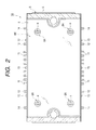
- FIG. 2 is a schematic bottom plan of the semiconductor device, which is Embodiment 1 of the present invention.
- FIG. 3 is a schematic bottom plan of a state in which part of the resin sealing body in FIG. 2 is removed.
- FIG. 4 is a schematic section along line A—A in FIG. 3 .
- FIG. 5 is a schematic section along line B—B in FIG. 3 .
- FIG. 6 is a schematic section along line C—C in FIG. 3 .
- FIG. 7 is a schematic section in which part of FIG. 5 is expanded.
- FIG. 8 is a schematic section illustrating a rough iconfiguration of the switching chip in FIG. 1 .
- FIG. 9 is a block diagram of an automobile circuit system into which the semiconductor device, which is Embodiment 1 of the invention is incorporated.
- FIG. 10 is a schematic plan of a lead frame for use in the manufacture of the semiconductor device, which is Embodiment 1 of the invention.
- FIG. 11 is a schematic bottom plan of a heat radiation plate for use in the manufacture of the semiconductor device, which is Embodiment 1 of the invention.
- FIG. 12 is a schematic plan for describing the manufacture of the semiconductor device, which is Embodiment 1 of the invention.
- FIG. 13 is another schematic plan of a lead frame for use in the manufacture of the semiconductor device, which is Embodiment 1 of the invention.
- FIG. 14 is still another schematic plan of a lead frame for use in the manufacture of the semiconductor device, which is Embodiment 1 of the invention.
- FIG. 15 is yet another schematic plan of a lead frame for use in the manufacture of the semiconductor device, which is Embodiment 1 of the invention.
- FIG. 16 is a schematic section of a semiconductor device, which is Embodiment 2 of the invention.
- FIG. 17 is a schematic bottom plan of the semiconductor device, which is Embodiment 3 of the invention.
- FIG. 18 is a schematic section of the semiconductor device, which is Embodiment 4 of the invention.
- FIG. 19 is a schematic section of the semiconductor device, which is Embodiment 5 of the invention.
- FIG. 20 is a schematic section of the semiconductor device, which is Embodiment 6 of the invention.
- FIG. 1 is a schematic plan of a semiconductor device, which is Embodiment 1 of the present invention.
- FIG. 2 is a schematic bottom plan of the semiconductor device of FIG. 1;
- FIG. 3 is a schematic bottom plan of a state in which part of the resin sealing body in FIG. 2 is removed;
- FIG. 4 is a schematic section along line A—A in FIG. 3;
- FIG. 5 is a schematic section along line B—B in FIG. 3;
- FIG. 6 is a schematic section along line C—C in FIG. 3;
- FIG. 7 is a schematic section in which part of FIG. 5 is expanded
- FIG. 8 is a schematic section illustrating a rough configuration of the switching chip in FIG. 1;
- FIG. 9 is a block diagram of an automobile circuit system into which the semiconductor device of FIG. 1 is incorporated.
- a semiconductor device 1 A in this embodiment has a configuration mainly comprising one control chip 2 with a built-in control circuit, four switching chips 3 with built-in switching elements, four fuse elements 4 whose fusible portions are fused by their own heat when an overcurrent flows, a heat radiation plate 5 on one of whose main surfaces is formed an insulating layer 6 , a resin sealing body 8 , a plurality of bonding wires ( 9 A, 9 B, 9 C), a plurality of lead ( 11 , 12 , 13 , 14 , 15 ), one die pad 16 , four die pads 17 and four pads ( 18 , 19 ).
- the plurality of leads may include, four instance four leads 11 , four leads 12 , four leads 13 , four leads 14 and two leads 15 .
- the switching elements are used power MOSFETs, which are insulating gate type field effect transistors. These power MOSFETs have a configuration in which a plurality of transistor cells are connected in parallel.
- the planar shape of the control chip 2 is quadrilaterally formed.
- the control chip 2 has a configuration in which, of mutually opposite main surfaces (one is the element forming surface and the other, the back surface), one has the control circuit and the plurality of electrode (bonding pads) 2 A.
- the control chip 2 has a configuration mainly comprising a semiconductor substrate made of monocrystalline silicon and a multilayer interconnection layer formed over this semiconductor substrate.
- the control circuit comprises a transistor element formed over one main surface (element forming surface) of the semiconductor substrate and wiring formed over the multilayer interconnection layer among other elements.
- Each of the plurality of electrodes 2 A is formed in the uppermost interconnection layer of the multilayer interconnection layer of the control chip 2 .
- the uppermost interconnection layer is covered with a surface protective layer (final protective layer), and in this surface protective layer is formed a bonding opening to expose the electrodes 2 A.
- the back surface of the control chip 2 is connected via adhesive 21 to one main surface of the die pad 16 in a state of opposing either of one main surface (chip mounting surface) and the other main surface (back surface) which oppose each other.
- the adhesive 21 may be, for instance, lead (Pb)-tin (Sn) solder, which excels in thermal conductivity.
- the planar shape of the four switching chips 3 is quadrilaterally formed.
- the four switching chips 3 have the same structure and the same function, though this similarity is not restricted.
- Each of the switching chips 3 has a configuration in which a power MOSFET (switching element), a gate electrode 40 and a source electrode 41 are arranged on either of one main surface (element forming surface) and the other main surface (back surface), and a drain electrode 42 on the other main surface.
- a power MOSFET switching element
- gate electrode 40 and a source electrode 41 are arranged on either of one main surface (element forming surface) and the other main surface (back surface), and a drain electrode 42 on the other main surface.
- the drain electrode 42 formed on the back surface of each switching chip 3 is adhered and fixed via adhesive 22 to one main surface of the matching die pad 17 in a state of opposing either of one main surface (chip mounting surface) and the other main surface (back surface) of the die pad 17 which oppose each other.
- the adhesive 22 may be, for instance, Pb—Sn solder, which excels in thermal conductivity.
- the switching chips 3 are connected in series to the mutually different fuse elements 4 .
- the power MOSFET of each switching chip 3 is subject to ON/OFF operations by the control circuit of the control chip 2 .
- power consumption by the control chip 2 is about 0.5 [W], for instance, and that of a switching chip 3 , about 3.0 [W].
- a switching chip 3 generates more heat than the control chip 2 does.
- Each switching chip 3 is configured mainly of a semiconductor substrate 30 , in which, for instance, an n ⁇ type semiconductor layer 30 B made of monocrystalline silicon is formed over one main surface of an n+ type semiconductor substrate 30 A made of monocrystalline silicon.
- a power MOSFET switching element
- This power MOSFET has an n-channel type vertical structure.
- the power MOSFET has a configuration mainly comprising a channel forming region, a gate insulating film 32 , gate conductor layer 33 , a source region and a drain region.
- the channel forming region is configured of a p type well region 35 formed in the n ⁇ type semiconductor layer 30 B.
- the source region is configured of an n+ type semiconductor region 36 formed in the p type well region 35 .
- the drain region is configured of the n ⁇ type semiconductor layer 30 B and the n+ type type semiconductor substrate 30 A.
- the gate insulating film 32 is formed of, for instance, silicon oxide, so as to cover the inner surface of a grooves 31 sinking from one main surface of the n ⁇ type semiconductor layer 30 B in the depthwise (thickness-wise) direction.
- the gate conductor layer 33 is embedded within the grooves 31 with the gate insulating film 32 in-between, and is formed of, for instance, a polycrystalline silicon film doped to reduce its resistance.
- the power MOSFET has a trench gate
- the element forming region of the main surface of the n ⁇ type semiconductor layer 30 B which is one main surface of the semiconductor substrate 30 , divided into a plurality of islands by the grooves 31 .
- This plurality of islands are regularly arranged in a matrix, and their planar shape is formed in a flat octagon.
- the gate conductor layer 33 is formed of a mesh pattern enclosing the plurality of islands partitioned by the grooves 31 .
- the n+ type semiconductor region 36 which is the source region, formed on one main surface of the islands partitioned by the grooves 31 .
- the n+ type semiconductor region 36 and the p type well region 35 are connected openings 38 , formed in an inter-layer insulating film 37 , to the source electrode 41 formed over them.
- the inter-layer insulating film 37 provided between the gate conductor layer 33 and the source electrode 41 , insulates and separates the gate conductor layer 33 and the source electrode 41 from each other.
- the source electrode 41 is formed of, for instance, a metallic film such as aluminum (Al) film or aluminum alloy film. Between the gate conductor layer 33 and the inter-layer insulating film 37 , there is formed an insulating film 34 .
- the gate conductor layer 33 is formed integrated with gate extraction wiring (not shown) provided over a peripheral region (inactive region) around one main surface of the n ⁇ type semiconductor layer 30 B via an insulating film.
- the gate extraction wiring is electrically connected through a port provided in the inter-layer insulating film 37 to a gate electrode 40 provided in the layer above the film.
- the gate electrode 40 is formed on the same layer as the source electrode 41 , and the source electrode 41 and the gate electrode 40 are insulated and separated from each other.
- a surface protective layer Over the source electrode 41 is formed a surface protective layer, and in this surface protective layer are provided a bonding port for exposing the source electrode 41 and another bonding port for exposing the gate electrode 40 .
- the drain electrode 42 is formed all over one main surface of the n+ type semiconductor substrate 30 A opposite to the other main surface, and electrically connected to the n+ type semiconductor substrate 30 A.
- the drain electrode 42 is formed of, for instance, an Au film.
- each of the four fuse elements 4 is electrically and mechanically connected to the mutually differing pads 18 and the other end is electrically and mechanically connected to the mutually differing pads 19 .
- Each of these four fuse elements 4 is formed of a fusible body made of, for instance, zinc (Zn).
- the four fuse element 4 have the same structure and the same function, though this similarity is not restricted.
- the planar shape of the heat radiation plate 5 is quadrilaterally formed, and in this embodiment is, for instance, a 50 [mm] ⁇ 24 [mm] rectangle.
- the heat radiation plate 5 has a thickness of, for instance, about 2 [mm], and formed of a metallic material of copper (Cu) or aluminum (Al) or an Cu or Al alloy, which excels in thermal conductivity.
- the planar shape of the resin sealing body 8 is quadrilaterally formed, and in this embodiment is, for instance, a 42 [mm] ⁇ 24 [mm] rectangle.
- the resin sealing body 8 is formed of an epoxy-based thermosetting resin to which, for instance, a phenol-based curing agent, silicone rubber, filler and the like are added.
- the resin sealing body 8 is formed by a transfer mold process, which is suitable for mass production.
- the transfer mold process is a method of forming a resin sealing body by which, using a mold die provided with a pot, runner, inlet gate, cavity and the like, thermosetting resin is poured into the cavity from the pot through the runner and the inlet gate.
- each of sixteen leads 11 and four leads ( 12 , 14 ) is configured to have an inner portion located within the resin sealing body 8 and an outer portion located outside the resin sealing body 8 .
- the outer portion of each of these leads ( 11 , 12 , 14 ) is bent and molded so that its tip be located on one main surface 8 X of two mutually opposite main surfaces of the resin sealing body 8 (one opposing one main surface of a switching chip).
- the outer portion of each of the leads ( 11 , 12 , 14 ) is configured as an external terminal for electrical connection to the outside.
- the main surface 8 X of the resin sealing body 8 when packaged into the semiconductor device 1 A, is opposite to the mounting surface of the mounting substrate.
- Each of the four leads 13 and two leads 15 is configured to have an inner portion located within the resin sealing body 8 and an outer portion located outside the resin sealing body 8 .
- the outer portion of each of these leads ( 13 , 15 ) unlike the outer portion of the lead 11 , is formed in such a length that it slightly protrudes from the resin sealing body 8 .
- the outer portions of the leads ( 13 , 15 ) are so configured as not to be electrically connected to the outside.
- the tips of the inner portions of the sixteen leads 11 , four leads 13 and four leads 14 are arranged around the die pad 16 so as to encircle the die pad 16 . These tips of the inner portions of the leads ( 11 , 13 , 14 ) are electrically connected by the bonding wire 9 A to the respectively matching electrodes 2 A of the control chip 2 .
- the gate electrodes 40 of the four switching chips 3 are electrically connected by the bonding wire 9 B to the respectively matching electrodes 2 A of the control chip 2 .
- the source electrodes 41 of the four switching chips 3 are electrically connected by the bonding wire 9 C to the intermediate portions of the inner portions of the respectively matching leads 13 .
- the four pads 18 are arranged near the respectively matching pads 17 .
- the bonding wires 9 A and 9 B are made of, for instance, gold (A u ), ant the bonding wire 9 C, of Al for instance.
- the bonding wires ( 9 A, 9 B, 9 C) are connected by, for instance, a ball bonding method, which combines thermocompression bonding with ultrasonic vibration.
- a single bonding wire 9 C is used for electrical connection of the source electrodes 41 of the switching chips 3 with the leads 13 in this embodiment, a plurality of bonding wires 9 C may as well be used for the electrical connection of these elements.
- the four die pads 17 are leads 12 .
- the four pads 18 are formed integrated with the inner portions of the respectively matching leads 13 .
- the four pads 19 are formed integrated with the inner portions of the respectively matching leads 14 .
- the control chip 2 four switching chips 3 , four fuse elements 4 , the plurality of bonding wires ( 9 A, 9 B, 9 C), inner portions of each of the plurality of leads ( 11 , 12 , 13 , 14 , 15 ), the die pad 16 , four die pads 17 and four pads ( 18 , 19 ) and so forth are arranged on one main surface of the heat radiation plate 6 , and sealed by the single resin sealing body 8 .
- the resin sealing body 8 is formed so as to cover one main surface of the heat radiation plate 5 and fixed to the heat radiation plate 6 .
- the inner portions of the plurality of leads ( 11 , 12 , 13 , 14 , 15 ), the plurality of die pads ( 16 , 17 ) and the plurality of pads ( 18 , 19 ) are arranged in isolation from the insulating layer 6 formed over one main surface of the heat radiation plate 5 .
- the resin of the resin sealing body 8 is interposed between these inner portions of the leads, die pads and pads on the one hand and the insulating layer 6 on the other.
- the insulating layer 6 is provided to keep from coming in contact with the heat radiation plate 5 , because the positions of the inner portions of the leads, die pads and pads, are varied vertically by the fluidity of the resin injected under pressure into the cavity of the mold die when the resin sealing body 8 is formed by the transfer mold process.
- the insulating layer 6 in order to secure a sufficient dielectric strength (AC2 [KV]), is formed to a thickness of, for instance 0.08 to 0.1 [mm].
- the insulating layer 6 is formed, of an insulating film made of, for instance, an epoxy thermosetting resin.
- the plurality of leads are divided into two groups of leads.
- the outer portions of one group of leads are arranged along one of the two opposing long sides of the resin sealing body 8 , and those of the other group of leads are arranged along the other long side of the resin sealing body 8 .
- the semiconductor device 1 A embodying the invention as described here, has a DIP (Dual In-line Package) type configuration.
- the control chip 2 is arranged in the central portion (an inside portion away from the periphery) of the resin sealing body 8 .
- the four switching chips 3 are arranged around the control chip 2 (between the periphery of the resin sealing body 8 and the control chip 2 ) so as to encircle the control chip 2 .
- the switching chip 3 generates a greater quantity of heat than the control chip 2 .
- thermal resistance is less on the periphery than in the central portion.
- the length of the bonding wire 9 B to electrically connect one electrode 2 A of the control chip 2 to the gate electrode 40 of one switching chip 3 is kept from becoming excessively longer than those of the other bonding wires 9 B electrically connecting the electrodes 2 A of the control chip 2 to the gate electrodes 40 of the other switching chips 3 .
- the four switching chips 3 are arranged symmetrically with respect to the control chip 2 .
- the four switching chips 3 are separately arranged outside the four corners of the control chip 2 . This configuration secures ample spacing between the switching chips 3 , making it possible to restrain thermal interference between adjacent switching chips 3 .
- the four fuse elements 4 are arranged around the control chip 2 so as to encircle the control chip 2 outside the switching chips 3 .
- This configuration serves to reduce the lengths of the bonding wires 9 B electrically connecting the electrodes 2 A of the control chip 2 to the gate electrodes 40 of the switching chips 3 compared with the lengths that would be required in the arrangement of the fuse elements 4 between the control chip 2 and the switching chips 3 , thereby facilitating faster ON/OFF operation control of the power MOSFET.
- the thermal impact on the fuse elements 4 of heat generated by the chips can be restrained, with the result that the fusing currents of the fuse elements 4 can be stabilized.
- the four fuse elements 4 are arranged symmetrically with respect to the control chip 2 .
- the four fuse elements 4 are separately arranged outside the four corners of the control chip 2 farther out than the switching chips 3 . This configuration secures ample spacing between the fusing elements 4 , making it possible to restrain thermal interference between adjacent fuse elements 4 .
- the one die pad 16 and the four die pads 17 are dispersed from one another.
- the control chip 2 is adhered and fixed to the die pad 16 isolated from the four die pads 17
- the four switching chips 3 are separately adhered and fixed to the four die pads 17 isolated from one another. Since the die pad 16 to which the control chip 2 is adhered and fixed is separated from the die pads 17 to which the switching chips 3 are adhered and fixed, the switching chips 3 are hard to be transferred to the control chip 2 , and thereby facilitates restraining of the impact of heat from the switching chips 3 on the control chip 2 .
- the separation of the four die pads 17 to which the four switching chips 3 are individually adhered and fixed from one another makes it difficult for heat from any one switching chip 3 to be transferred to the other switching chips 3 , and thereby facilitates restraining of the impact of heat from any one switching chip 3 on the other switching chips 3 .
- the heat radiation plate 5 has a configuration in which the through holes 7 penetrating from one main surface to the other are provided. Since four fuse elements 4 are provided in this embodiment, the number of the through holes 7 is also four. Further in this embodiment, as the insulating layer 6 is provided over one main surface of the heat radiation plate 5 , the insulating layer 6 also has through holes similar to the through holes 7 in the parts respectively opposite to the fuse elements 4 . This arrangement makes it difficult for heat transferred to the heat radiation plate 5 to be transferred to the fuse elements 4 as well as for heat from the fuse elements 4 to be transferred to the heat radiation plate 5 , resulting in stabilization of the fusing currents of the fuse elements 4 .
- the resin sealing body 8 is so configured as to have, in the portions opposite to the fuse elements 4 , the concave portions 8 A sinking from one main surface 8 X of the resin sealing body 8 opposite to one main surface of each of the switching chips 3 toward the fuse elements 4 and the concave portions 8 B sinking from the other main surface opposite to one main surface of the resin sealing body 8 toward the fuse elements 4 . Since the semiconductor device 1 A embodying the invention as described here is a package structure having the heat radiation plate 5 , the concave portions 8 B are formed through the through holes 7 provided in the heat radiation plate 5 .
- the concave portions 8 A and the concave portions 8 B are formed in a sufficient depth for the intermediate parts of the fuse elements 4 to be exposed from the bottoms of the concave portions. This arrangement makes it difficult for heat transferred to the resin sealing body 8 to be transferred to the fuse elements 4 as well as for heat from the fuse elements 4 to be transferred to the resin sealing body 8 , resulting in stabilization of the fusing currents of the fuse elements 4 .
- the semiconductor device 1 A configured in this way can be incorporated into, for instance as shown in FIG. 9, into an automobile circuit system.
- a reference numeral 50 denotes a power source (e.g., a 12 [V] battery), and 51 , loads (e.g., motors to drive power windows, drive motors for intermittent window wipers, engine control system and lighting system)
- loads e.g., motors to drive power windows, drive motors for intermittent window wipers, engine control system and lighting system
- the semiconductor device 1 A outputs from its control chip (control circuit) 2 switch drive signals for ON/OFF operation control of various switching chips (power MOSFETs) 3 on the basis of input signals, and thereby controls current supply to the loads 51 .
- control chip control circuit
- FIG. 10 is a schematic plan of the lead frame
- FIG. 11, a schematic bottom plan of the heat radiation plate.
- FIG. 10 and FIG. 11 illustrate only one region each for the manufacture of one semiconductor device to make the illustrations easier to understand.
- a lead frame LF has a configuration in which mainly a plurality of leads ( 11 , 12 , 13 , 14 , 15 ), one die pad 16 , four die pads 17 , four pads ( 18 , 19 ) and the like are arranged in a lead arrangement region whose plane is defined quadrilaterally (in a rectangle in this embodiment) by a frame body 10 .
- the plurality of leads are divided into two groups of leads.
- One group of leads (eight leads 11 and two leads ( 12 , 13 , 14 )) are arranged along one of the two opposing long sides of the frame body 10 , and those of the other group of leads (eight leads 11 and two leads ( 12 , 13 , 14 ) are arranged along the other long side of the frame body 8 .
- individual leads are integrated by a dam bar (also known as tie bar) 20 , and leads 14 located at the initial and final stages of the lead arrangement are integrated with the short side portions of the frame body 10 by the dam bar 20 .
- the outer portions of the other leads than the leads 13 and 15 are integrated with one long side portion of the frame body 10 .
- the lead frame LF has a bidirectional lead arrangement structure.
- the planar shape of the die pad 16 is quadrilaterally formed.
- the die pad 16 is formed integrated with each of two leads 15 arranged opposite to each other.
- Each of the die pads 17 is formed integrated with the matching lead 12 ;
- each of the die pads 18 is formed integrated with the matching lead 13 ; and
- each of the pads 19 is formed integrated with the matching lead 14 .
- Each of the pads 18 is arranged near the matching pad 19 .
- the die pad 16 is disposed in the central portion of the lead arrangement region.
- the four die pads 17 are arranged around the die pad 16 so as to encircle the die pad 16 .
- the four pads ( 18 , 19 ), located farther out than the four die pads 17 are arranged around the die pad 16 so as to encircle the die pad 16 .
- the four die pads 17 are separately arranged outside the four corners of the die pad 16 .
- the four pads ( 18 , 19 ) are separately arranged outside the four corners of the die pad 16 farther out than the die pad 17 .
- the lead frame LF is formed by either etching or pressing a planar sheet of, for instance, iron (Fe) -nickel (Ni) alloy, or Cu or a Cu ally into prescribed leads and pads.
- the lead frame LF is formed in a thickness of, for instance, about 0.45 [mm].
- the lead frame LF is configured to have four fuse elements 4 .
- One end of each fuse element 4 is electrically and mechanically connected to the matching pad 18 and the other end is electrically and mechanically connected to the matching pad 19 .
- the heat radiation plate 5 before being subjected to a manufacturing process has a configuration comprising a product portion 5 L to be used as the product and removable portions SM to be cut and removed in the manufacturing process.
- the removable portions 5 M are on both sides, in the lengthwise direction, of the product portion 5 L.
- the insulating layer 6 Over one main surface of the heat radiation plate 5 is formed the insulating layer 6 so as to cover this whole main surface.
- the through holes 7 are disposed in positions opposite to the fuse elements 4 .
- the removable portion 5 M of the heat radiation plate 5 are provided through holes 7 A penetrating the heat radiation plate 5 from one of its main surfaces to the other, and the insulating layer 6 also has through holes similar to these through holes 7 A in the parts respectively matching these through holes 7 A.
- the through holes 7 A are used for positioning when the heat radiation plate 5 is fitted to the mold die.
- a package having the heat radiation plate 5 requires efficient transferring of heat from chips to the heat radiation plate. Efficient transferring of heat from chips to the heat radiation plate can be achieved by narrowing the gaps between the die pads ( 16 , 17 ) on which the chips are mounted and the heat radiation plate 5 .
- the insulating layer 6 is formed over one main surface of the heat radiation plate 5 to prevent the heat radiation plate 5 from coming into contact with the inner portions of the leads and the die pads on this main surface of the heat radiation plate 5 , the gaps between the die pads and the insulating layer 6 should be kept as narrow as practicable.
- the gaps between the die pads and the insulating layer 6 are made too much narrower than the grain size of the fillers, the gaps between the die pads and the insulating layer 6 will fail to be filled with the resin, and the gaps will remain void. If void gaps are formed, the thermal resistance between the die pads and the insulating layer 6 will rather increase. Moreover, there will arise the trouble of crack generation in the resin sealing body, starting from the void gaps.
- epoxy thermosetting resin containing many fillers whose grain size, for instance, 3 to 5 [ ⁇ m] on the average and 25 [ ⁇ m] at the maximum is used for the resin sealing body 8 and die pads of, for instance, about 0.45 [mm] in thickness are used, the gaps between the die pads and the insulating layer 6 are set to, for instance, around 0.2 [mm].
- FIG. 12 and FIG. 13 are schematic plans illustrating the manufacture
- FIG. 14 and FIG. 15 are schematic sections illustrating the manufacture.
- the lead frame LF and the heat radiation plate 5 shown in FIG. 10 are prepared and, after that, the control chip 2 is adhered and fixed to the die pad 16 of the lead frame LF while the switching chips 3 are adhered and fixed to the respectively matching ones of the four die pads 17 of the lead frame LF.
- the die pad 16 and the control chip 2 are adhered and fixed to each other via the adhesive 21 applied between one main surface of the die pad 16 and the back surface of the control chip 2 .
- the die pads 17 and the switching chips 3 are adhered and fixed to each other via the adhesive 22 applied between the die pads 17 and the drain electrodes 42 on the back surfaces of the switching chips 3 .
- the tips of the inner portions of the leads are electrically connected to the respectively matching electrodes 2 A of the control chip 2 with the bonding wires 9 A; the gate electrodes 40 of the switching chips 3 are electrically connected to the respectively matching electrodes 2 A of the control chip 2 with the bonding wires 9 B; and the source electrodes 41 of the switching chips 3 are electrically connected to the central parts of the inner portions of the respectively matching leads 13 with the bonding wires 9 C.
- the lead frame LF and the heat radiation plate 5 are positioned between an upper die 45 A and a lower die 45 B of a mold die 45 . Then, within a cavity 46 formed by the upper die 45 A and the lower 45 B, the control chip 2 , switching chips 3 , fuse elements 4 , heat radiation plate 5 , inner portions of the leads ( 11 , 12 , 13 , 14 , 15 ), die pads ( 16 , 17 ), pads ( 18 , 19 ), bonding wires ( 9 A, 9 B, 9 C) and so forth are arranged.
- the lead frame LF and the heat radiation plate 5 are so positioned as to arrange the inner portions of the leads, die pads and pads over one main surface (the surface over which the insulating layer 6 is formed) of the heat radiation plate 5 . They are also so positioned as to leave some gaps between the inner portions of the leads, die pads and pads on the one hand and the insulating layer 6 on the other.
- the gaps are kept greater than the maximum grain size of the fillers mixed into the resin used for forming the resin sealing body but narrower than the thickness of the lead frame LF (die pads). In this embodiment, the gaps are set to, for instance, around 0.2 [mm].
- the mold die 45 has a configuration in which there are, in its portions opposite to the fuse elements 4 , protruding portions 47 A protruding from the inner wall face side of the cavity 46 opposite to the fuse elements 4 toward the switching chips 3 and protruding portions 47 B protruding from the inner wall face side of the cavity 46 opposite to the back surfaces of die pads and the back surfaces of the heat radiation plate 5 toward the fuse elements 4 .
- the protruding portions 47 A and 47 B have mechanisms to allow adjustment of the extents of protrusion from the inner wall face side of the cavity 46 toward the fuse elements 4 .
- fluid resin is poured under pressure from the pot of the mold die 45 through the runner and the inlet gate into the cavity 46 to form the resin sealing body 8 .
- control chip 2 switching chips 3 , fuse elements 4 , plurality of bonding wires ( 9 A, 9 B, 9 C), respective inner portions of the plurality of lead ( 11 , 12 , 13 , 14 , 15 ), die pad 16 , die pads 17 , pads ( 18 , 19 ) and so forth are sealed by the resin sealing body 8 .
- the resin sealing body 8 having, in the portions opposite to the fuse elements 4 , the concave portions 8 A sinking from one main surface 8 X of the resin sealing body 8 opposite to one main surface of each of the switching chips 3 toward the fuse elements 4 and the concave portions 8 B sinking from the other main surface opposite to one main surface of the resin sealing body 8 through the through holes 7 toward the fuse elements 4 .
- the concave portions 8 A and the concave portions 8 B are formed in a sufficient depth for the intermediate ports of the fuse elements 4 to be exposed from the bottoms of the concave portions.
- any of the bonding wires 9 B is substantially prevented from becoming excessively longer than any other bonding wire 9 B, the occurrence of short circuiting trouble due to any wire flow of the bonding wire 9 B can be restrained.
- gaps between the inner portions of the leads, die pads and pads on the one hand and the insulating layer 6 on the other are kept greater than the maximum grain size of the fillers mixed into the resin, no void gaps due to the resin mixed into the fillers occur between them.
- control chip 2 is arranged in the central portion of the resin sealing body 8 , and the four switching chips 3 are arranged on the periphery of the control chip 2 .
- the length of the bonding wire 9 B to electrically connect one electrode 2 A of the control chip 2 to the gate electrode 40 of one switching chip 3 is kept from becoming excessively longer than those of the other bonding wires 9 B electrically connecting the electrodes 2 A of the control chip 2 to the gate electrodes 40 of the other switching chips 3 .
- the four switching chips 3 are arranged symmetrically with respect to the control chip 2 In this embodiment, the four switching chips 3 are separately arranged outside the four corners of the control chip 2 .
- the four fuse elements 4 are arranged around the control chip 2 farther out than the switching chips 3 .
- This configuration serves to reduce the lengths of the bonding wires 9 B electrically connecting the electrodes 2 A of the control chip 2 to the gate electrodes 40 of the switching chips 3 compared with the lengths that would be required in the arrangement of the fuse elements 4 between the control chip 2 and the switching chips 3 , thereby facilitating faster ON/OFF operation control of the power MOSFET.
- the reduced lengths of the bonding wires 9 B serves to reduce short circuiting trouble due to the hanging of any bonding wire 9 B and short circuiting trouble due to wire fluidity.
- the thermal impact on the fuse elements 4 of heat generated by the chips can be restrained, and accordingly the fusing currents of the fuse elements 4 can be stabilized, with the result that the reliability of the semiconductor device 1 A can be enhanced.
- the four fuse elements 4 are arranged symmetrically with respect to the control chip 2 .
- the four fuse elements 4 are separately arranged outside the four corners of the control chip 2 farther out than the switching chips 3 . This configuration secures ample spacing between the fusing elements 4 , making it possible to restrain thermal interference between adjacent fuse elements 4 , with the result that the reliability of the semiconductor device 1 A can be enhanced.
- the die pad 16 to which the control chip 2 is adhered and fixed is separated from the four die pads 17 to which the four switching chips 3 are adhered and fixed from one another, and this configuration makes it difficult for heat from thee switching chips 3 to be transferred to the control chip 2 , and thereby facilitates restraining of the impact of heat from thee switching chip 3 on the control chip 2 . As a result, the reliability of the semiconductor device 1 A can be enhanced.
- the four die pads 17 to which the four switching chips 3 are adhered and fixed are separated from one another. This configuration makes it difficult for heat from any one switching chip 3 to be transferred to the other switching chips 3 , and thereby facilitates restraining of the impact of heat from any one switching chip 3 on the other switching chips 3 . As a result, the reliability of the semiconductor device 1 A can be enhanced.
- the heat radiation plate 5 is provided, in its portion opposite to the fuse elements 4 , with the through holes 7 penetrating the heat radiation plate 5 from one of its main surfaces to the other.
- This configuration makes it difficult for heat transferred to the heat radiation plate 5 to be transferred to the fuse elements 4 and the heat from the fuse elements 4 to be transferred to the heat radiation plate 5 , and thereby facilitates stabilization of the fusing currents of the fuse elements 4 .
- the reliability of the semiconductor device 1 A can be enhanced.
- the resin sealing body 8 has, in the portions opposite to the fuse elements 4 , the concave portions 8 A sinking from one main surface 8 X of the resin sealing body 8 opposite to one main surface of each of the switching chips 3 toward the fuse elements 4 and the concave portions 8 B sinking from the other main surface opposite to one main surface of the resin sealing body 8 toward the fuse elements 4 .
- this configuration makes it difficult for heat transferred to the resin sealing body 8 to be transferred to the fuse elements 4 as well as for heat from the fuse elements 4 to be transferred to the resin sealing body 8 , resulting in stabilization of the fusing currents of the fuse elements 4 .
- the resin sealing body 8 is formed by injecting resin under pressure into the cavity 46 .
- the fuse elements 4 may as well be connected in the assembling process of the semiconductor device.
- the resin sealing body 8 may have only either the concave portions 8 A or the concave portions 8 B.
- each switching chip may as well have the gate electrode and the drain electrode on one main surface and the source electrode on the other main surface.
- each switching chip 3 may as well have a horizontally structured power MOSFET built into it.
- switching chips 3 with built-in power MOSFETs as insulating gate type field effect transistors
- switching chips 3 with built-in power MISFETs Metal Insulator Semiconductor Field Effect Transistors
- the four switching chips 3 used in this embodiment described here have the same structure and the same functions, the four switching chips may as well have different structures and different functions.
- the four fuse elements 4 used in this embodiment described here have the same structure and the same functions, the four fuse elements 4 may as well have different structures and different functions.
- FIG. 16 is a schematic section of a semiconductor device, which is Embodiment 2 of the present invention.
- a semiconductor device 1 B embodying the invention in this way has basically the same configuration as Embodiment 1 described except in the following aspects.
- each fuse element 4 has a smaller sectional area in one intermediate portion 4 A than elsewhere.
- a groove is formed in the portion 4 A to reduce the sectional area of that portion. This configuration serves to fix the fusible portion of the fuse element 4 in one location, and thereby contributes to further stabilizing the fusing current of the fuse element 4 .
- the sectional area of the portion 4 A can be made smaller by reducing its width.
- FIG. 17 is a schematic bottom plan of the semiconductor device, which is Embodiment 3 of the present invention.
- a semiconductor device 1 C embodying the invention in this way has basically the same configuration as Embodiment 1 described except in the following aspects.
- each of the concave portions 8 A and the concave portions 8 B is formed in such a depth that the resin of the resin sealing body 8 intervenes between its bottom surface and the intermediate portion of a fuse element 4 (such a depth that its bottom surface is isolated from the intermediate portion of the fuse element 4 ).
- Such concave portions 8 A and concave portions 8 B can be readily formed by adjusting the extents of protrusion of the protruding portions 47 A and 47 B (see FIG. 15) during the formation process of the resin sealing body.
- This configuration can help stabilize the fusing currents of the fuse elements 4 .
- the fusing currents of the fuse elements 4 can be controlled with the depths of the concave portions 8 A and the concave portions 8 B.
- FIG. 18 is a schematic section of the semiconductor device, which is Embodiment 4 of the present invention.
- a semiconductor device 1 D embodying the invention in this way has basically the same configuration as Embodiment 3 described except in the following aspects.
- each fuse element 4 as in Embodiment 2 described above, has a smaller sectional area in one intermediate portion 4 A than elsewhere. This configuration contributes to further stabilizing the fusing current of the fuse element 4 .
- FIG. 19 is a schematic section of the semiconductor device, which is Embodiment 5 of the present invention.
- a semiconductor device 1 E embodying the invention in this way has basically the same configuration as Embodiment 1 described except in the following aspects.
- each fuse element 4 is coated with a resin 51 having a lower thermal conductivity than the resin of the resin sealing body 8 .
- a resin 51 for instance, a silicon resin having a thermal conductivity of about 0.2 [W/mK] is used. This configuration makes it difficult for heat transferred to the resin sealing body 8 to be transferred to the fuse elements 4 as well as for heat from the fuse elements 4 to be transferred to the resin sealing body 8 , resulting in stabilization of the fusing currents of the fuse elements 4 .
- FIG. 20 is a schematic section of the semiconductor device, which is Embodiment 6 of the present invention.
- a semiconductor device 1 E embodying the invention in this way has basically the same configuration as Embodiment 1 described except in the following aspects.
- the pads 18 and 19 are exposed from the bottom surfaces of the concave portions 8 A and the concave portions 8 B, and no fuse elements are connected to the pads 18 and 19 .
- This configuration enables the fuse elements and other components to be connected to the pads 18 and 19 after the resin sealing body 8 has been formed.
Abstract
Description
Claims (18)
Applications Claiming Priority (2)
| Application Number | Priority Date | Filing Date | Title |
|---|---|---|---|
| JP2000151866A JP3737673B2 (en) | 2000-05-23 | 2000-05-23 | Semiconductor device |
| JP2000-151866 | 2000-05-23 |
Publications (2)
| Publication Number | Publication Date |
|---|---|
| US20010048148A1 US20010048148A1 (en) | 2001-12-06 |
| US6441484B2 true US6441484B2 (en) | 2002-08-27 |
Family
ID=18657357
Family Applications (1)
| Application Number | Title | Priority Date | Filing Date |
|---|---|---|---|
| US09/859,408 Expired - Fee Related US6441484B2 (en) | 2000-05-23 | 2001-05-18 | Semiconductor device having switching elements around a central control circuit |
Country Status (4)
| Country | Link |
|---|---|
| US (1) | US6441484B2 (en) |
| JP (1) | JP3737673B2 (en) |
| KR (1) | KR20010107556A (en) |
| TW (1) | TW561609B (en) |
Cited By (5)
| Publication number | Priority date | Publication date | Assignee | Title |
|---|---|---|---|---|
| KR20010107556A (en) * | 2000-05-23 | 2001-12-07 | 가나이 쓰토무 | A Semiconductor Device and A Method of Manufacturing the Same |
| US6630748B2 (en) * | 2001-02-06 | 2003-10-07 | Denso Corporation | Load control apparatus and method having single temperature detector |
| US20050185353A1 (en) * | 2003-06-06 | 2005-08-25 | Electronic Theatre Controls, Inc. | Overcurrent protection for solid state switching system |
| US20080160677A1 (en) * | 2005-10-19 | 2008-07-03 | Tong Soon Hock | Method of Forming Component Package |
| US20080247142A1 (en) * | 2005-12-28 | 2008-10-09 | Kuno Wolf | Electronic Module and Method for Producing Such a Module |
Families Citing this family (20)
| Publication number | Priority date | Publication date | Assignee | Title |
|---|---|---|---|---|
| JP2003100986A (en) * | 2001-09-26 | 2003-04-04 | Toshiba Corp | Semiconductor device |
| JP2003264265A (en) * | 2002-03-08 | 2003-09-19 | Mitsubishi Electric Corp | Power semiconductor device |
| JP4246598B2 (en) * | 2003-10-22 | 2009-04-02 | 三菱電機株式会社 | Power semiconductor device |
| JP4610283B2 (en) * | 2004-09-30 | 2011-01-12 | 三洋電機株式会社 | Semiconductor device |
| US8269338B2 (en) * | 2006-08-10 | 2012-09-18 | Vishay General Semiconductor Llc | Semiconductor device having improved heat dissipation capabilities |
| US8048714B2 (en) * | 2006-08-11 | 2011-11-01 | Vishay General Semiconductor Llc | Semiconductor device and method for manufacturing a semiconductor device having improved heat dissipation capabilities |
| DE102007020618B8 (en) * | 2007-04-30 | 2009-03-12 | Danfoss Silicon Power Gmbh | Method for producing a solid power module and transistor module made therewith |
| JP5067151B2 (en) * | 2007-12-19 | 2012-11-07 | 株式会社デンソー | Mold package manufacturing method |
| JP5125758B2 (en) * | 2008-05-19 | 2013-01-23 | 三菱電機株式会社 | Resin-sealed semiconductor device and manufacturing method thereof |
| DE102008064428B4 (en) | 2008-12-22 | 2016-02-25 | Austriamicrosystems Ag | Chip structure and method for producing a chip structure |
| DE102010002950A1 (en) * | 2010-03-17 | 2011-09-22 | Robert Bosch Gmbh | CIRCUIT ARRANGEMENT AND ASSOCIATED CONTROL UNIT FOR A MOTOR VEHICLE |
| JP5261851B2 (en) * | 2010-04-08 | 2013-08-14 | 三菱電機株式会社 | Manufacturing method of semiconductor device |
| JP5099243B2 (en) | 2010-04-14 | 2012-12-19 | 株式会社デンソー | Semiconductor module |
| JP2013070026A (en) | 2011-09-08 | 2013-04-18 | Rohm Co Ltd | Semiconductor device, manufacturing method of semiconductor device, mounting structure of semiconductor device, and power semiconductor device |
| JP5354058B2 (en) * | 2012-05-15 | 2013-11-27 | 三菱電機株式会社 | Resin-sealed semiconductor device |
| JP6660278B2 (en) * | 2016-10-26 | 2020-03-11 | 三菱電機株式会社 | Resin-sealed semiconductor device |
| CN111066116B (en) * | 2017-08-30 | 2022-05-17 | 三菱电机株式会社 | Power conversion device |
| JP6992399B2 (en) * | 2017-10-19 | 2022-01-13 | 株式会社デンソー | Semiconductor module |
| JP7154907B2 (en) * | 2018-09-14 | 2022-10-18 | 株式会社東芝 | semiconductor module |
| JP7312604B2 (en) * | 2019-05-13 | 2023-07-21 | ローム株式会社 | semiconductor equipment |
Citations (5)
| Publication number | Priority date | Publication date | Assignee | Title |
|---|---|---|---|---|
| JPH05234495A (en) | 1992-02-25 | 1993-09-10 | Hitachi Ltd | Semiconductor device |
| US5362984A (en) * | 1991-02-28 | 1994-11-08 | Nippon Steel Corporation | Semiconductor device with jumping wire |
| JPH0758293A (en) | 1993-08-18 | 1995-03-03 | Hitachi Ltd | Insulated-gate semiconductor device, and drive circuit device and electronic system using same |
| US5604674A (en) * | 1994-08-10 | 1997-02-18 | Fuji Electric Co., Ltd. | Driving circuit module |
| US5642952A (en) | 1995-07-06 | 1997-07-01 | Brother Kogyo Kabushiki Kaisha | Sheet-supply unit capable of controlling sheet-feed operations and sheet alignment operations using a single solenoid |
Family Cites Families (5)
| Publication number | Priority date | Publication date | Assignee | Title |
|---|---|---|---|---|
| JP2601228B2 (en) * | 1994-11-18 | 1997-04-16 | サンケン電気株式会社 | Method for manufacturing resin-sealed circuit device |
| JPH09186287A (en) * | 1995-12-28 | 1997-07-15 | Shindengen Electric Mfg Co Ltd | Semiconductor device |
| KR19980027881A (en) * | 1996-10-18 | 1998-07-15 | 김광호 | Smart Power Transistor Package with Insulated Board |
| JPH11233712A (en) * | 1998-02-12 | 1999-08-27 | Hitachi Ltd | Semiconductor device, its manufacture and electric apparatus using the semiconductor device |
| JP3737673B2 (en) * | 2000-05-23 | 2006-01-18 | 株式会社ルネサステクノロジ | Semiconductor device |
-
2000
- 2000-05-23 JP JP2000151866A patent/JP3737673B2/en not_active Expired - Fee Related
-
2001
- 2001-04-30 KR KR1020010023311A patent/KR20010107556A/en not_active Application Discontinuation
- 2001-05-18 US US09/859,408 patent/US6441484B2/en not_active Expired - Fee Related
- 2001-05-23 TW TW090112433A patent/TW561609B/en not_active IP Right Cessation
Patent Citations (5)
| Publication number | Priority date | Publication date | Assignee | Title |
|---|---|---|---|---|
| US5362984A (en) * | 1991-02-28 | 1994-11-08 | Nippon Steel Corporation | Semiconductor device with jumping wire |
| JPH05234495A (en) | 1992-02-25 | 1993-09-10 | Hitachi Ltd | Semiconductor device |
| JPH0758293A (en) | 1993-08-18 | 1995-03-03 | Hitachi Ltd | Insulated-gate semiconductor device, and drive circuit device and electronic system using same |
| US5604674A (en) * | 1994-08-10 | 1997-02-18 | Fuji Electric Co., Ltd. | Driving circuit module |
| US5642952A (en) | 1995-07-06 | 1997-07-01 | Brother Kogyo Kabushiki Kaisha | Sheet-supply unit capable of controlling sheet-feed operations and sheet alignment operations using a single solenoid |
Non-Patent Citations (1)
| Title |
|---|
| 2.5 V-Driven Type 3rd Generation Trench Gate MOSFET, in Toshiba Review, vol. 53, No. 11 (1998), pp. 45-47. (Month Unknown). |
Cited By (8)
| Publication number | Priority date | Publication date | Assignee | Title |
|---|---|---|---|---|
| KR20010107556A (en) * | 2000-05-23 | 2001-12-07 | 가나이 쓰토무 | A Semiconductor Device and A Method of Manufacturing the Same |
| US6630748B2 (en) * | 2001-02-06 | 2003-10-07 | Denso Corporation | Load control apparatus and method having single temperature detector |
| US20050185353A1 (en) * | 2003-06-06 | 2005-08-25 | Electronic Theatre Controls, Inc. | Overcurrent protection for solid state switching system |
| US7369386B2 (en) * | 2003-06-06 | 2008-05-06 | Electronic Theatre Controls, Inc. | Overcurrent protection for solid state switching system |
| US20080160677A1 (en) * | 2005-10-19 | 2008-07-03 | Tong Soon Hock | Method of Forming Component Package |
| US7723165B2 (en) * | 2005-10-19 | 2010-05-25 | Infineon Technologies Ag | Method of forming component package |
| US20080247142A1 (en) * | 2005-12-28 | 2008-10-09 | Kuno Wolf | Electronic Module and Method for Producing Such a Module |
| US8169791B2 (en) | 2005-12-28 | 2012-05-01 | Robert Bosch Gmbh | Electronic module and method for producing such a module |
Also Published As
| Publication number | Publication date |
|---|---|
| TW561609B (en) | 2003-11-11 |
| KR20010107556A (en) | 2001-12-07 |
| JP3737673B2 (en) | 2006-01-18 |
| US20010048148A1 (en) | 2001-12-06 |
| JP2001332687A (en) | 2001-11-30 |
Similar Documents
| Publication | Publication Date | Title |
|---|---|---|
| US6441484B2 (en) | Semiconductor device having switching elements around a central control circuit | |
| CN211238167U (en) | Semiconductor device with a plurality of transistors | |
| US7586180B2 (en) | Semiconductor packaging device comprising a semiconductor chip including a MOSFET | |
| US7800208B2 (en) | Device with a plurality of semiconductor chips | |
| US6423623B1 (en) | Low Resistance package for semiconductor devices | |
| KR100342589B1 (en) | Semiconductor power modules and methods for manufacturing the same | |
| KR101418397B1 (en) | Semiconductor package, and method for fabricating the same | |
| US6396138B1 (en) | Chip array with two-sided cooling | |
| US20070045785A1 (en) | Reversible-multiple footprint package and method of manufacturing | |
| US20030075783A1 (en) | Semiconductor device | |
| US7091603B2 (en) | Semiconductor device | |
| US8723300B2 (en) | Multi-chip module power clip | |
| KR20070066970A (en) | Package for high power density device | |
| JPH0350758A (en) | Resin seal type semiconductor device | |
| EP0206771B1 (en) | Packaged semiconductor device | |
| US5616886A (en) | Wirebondless module package | |
| JPH10261756A (en) | Semiconductor device and its manufacture | |
| JP3877409B2 (en) | Manufacturing method of semiconductor device | |
| US6140702A (en) | Plastic encapsulation for integrated circuits having plated copper top surface level interconnect | |
| US20220199563A1 (en) | High thermal dissipation, packaged electronic device and manufacturing process thereof | |
| US20030228720A1 (en) | Semiconductor device and a method of manufacturing the same | |
| US6140150A (en) | Plastic encapsulation for integrated circuits having plated copper top surface level interconnect | |
| EP0415106B1 (en) | Lead frames for semiconductor device | |
| JP4277168B2 (en) | Resin-sealed semiconductor device and manufacturing method thereof | |
| EP3944309A1 (en) | Packaged high voltage mosfet device with a dbc interconnection substrate and manufacturing process thereof |
Legal Events
| Date | Code | Title | Description |
|---|---|---|---|
| AS | Assignment |
Owner name: HITACHI, LTD., JAPAN Free format text: ASSIGNMENT OF ASSIGNORS INTEREST;ASSIGNORS:KOYAMA, KENJI;ARAI, NORINAGA;MIKAMI, AKIO;AND OTHERS;REEL/FRAME:012929/0884 Effective date: 20010228 Owner name: HITACHI TOHBU SEMICONDUCTOR, LTD., JAPAN Free format text: ASSIGNMENT OF ASSIGNORS INTEREST;ASSIGNORS:KOYAMA, KENJI;ARAI, NORINAGA;MIKAMI, AKIO;AND OTHERS;REEL/FRAME:012929/0884 Effective date: 20010228 |
|
| FPAY | Fee payment |
Year of fee payment: 4 |
|
| FEPP | Fee payment procedure |
Free format text: PAYOR NUMBER ASSIGNED (ORIGINAL EVENT CODE: ASPN); ENTITY STATUS OF PATENT OWNER: LARGE ENTITY |
|
| FPAY | Fee payment |
Year of fee payment: 8 |
|
| AS | Assignment |
Owner name: RENESAS ELECTRONICS CORPORATION, JAPAN Free format text: ASSIGNMENT OF ASSIGNORS INTEREST;ASSIGNOR:HITACHI, LTD.;REEL/FRAME:026109/0976 Effective date: 20110307 |
|
| REMI | Maintenance fee reminder mailed | ||
| LAPS | Lapse for failure to pay maintenance fees | ||
| STCH | Information on status: patent discontinuation |
Free format text: PATENT EXPIRED DUE TO NONPAYMENT OF MAINTENANCE FEES UNDER 37 CFR 1.362 |
|
| FP | Lapsed due to failure to pay maintenance fee |
Effective date: 20140827 |