US6438624B1 - Configurable I/O expander addressing for I/O drawers in a multi-drawer rack server system - Google Patents
Configurable I/O expander addressing for I/O drawers in a multi-drawer rack server system Download PDFInfo
- Publication number
- US6438624B1 US6438624B1 US09/281,083 US28108399A US6438624B1 US 6438624 B1 US6438624 B1 US 6438624B1 US 28108399 A US28108399 A US 28108399A US 6438624 B1 US6438624 B1 US 6438624B1
- Authority
- US
- United States
- Prior art keywords
- logic component
- communications
- bus
- address
- input
- Prior art date
- Legal status (The legal status is an assumption and is not a legal conclusion. Google has not performed a legal analysis and makes no representation as to the accuracy of the status listed.)
- Expired - Lifetime
Links
Images

Classifications
-
- G—PHYSICS
- G06—COMPUTING; CALCULATING OR COUNTING
- G06F—ELECTRIC DIGITAL DATA PROCESSING
- G06F13/00—Interconnection of, or transfer of information or other signals between, memories, input/output devices or central processing units
- G06F13/38—Information transfer, e.g. on bus
- G06F13/42—Bus transfer protocol, e.g. handshake; Synchronisation
- G06F13/4282—Bus transfer protocol, e.g. handshake; Synchronisation on a serial bus, e.g. I2C bus, SPI bus
-
- G—PHYSICS
- G06—COMPUTING; CALCULATING OR COUNTING
- G06F—ELECTRIC DIGITAL DATA PROCESSING
- G06F2213/00—Indexing scheme relating to interconnection of, or transfer of information or other signals between, memories, input/output devices or central processing units
- G06F2213/0016—Inter-integrated circuit (I2C)
Definitions
- the present invention generally relates to electronic data communications and integrated circuits (ICs), and more particularly to a method of configuring input/output (I/O) expander addresses on a communications bus, to facilitate inter-IC communications among a plurality of I/O planars used in a computer system.
- ICs electronic data communications and integrated circuits
- I/O input/output
- a communications bus may be used to transmit certain values, such as data (operands) which are input to a logic component, or instructions used by the logic components, and further may be used to transmit various control signals.
- Buses can be unidirectional, bidirectional, or broadcast (used to interconnect three or more devices and allow simultaneous or sequential access to information or controls conveyed on the bus).
- These buses may be external, e.g., laid out on a printed circuit board, and interconnecting two or more devices which are separately packaged. They may also be internal, interconnecting two or more devices which are fabricated in a single package, such as an integrated circuit (IC).
- IC integrated circuit
- Buses are used to interconnect devices for a wide variety of applications, including communications between complex computer components such as microprocessors, application specific integrated circuits (ASICs), peripheral devices, random-access memory, etc.
- ASICs application specific integrated circuits
- Several different external bus designs have been developed for interconnecting various computer components. Early designs include the “expansion” bus referred to as the XT bus, and the later AT bus, also referred to as the Industry Standard Architecture (ISA) bus. A 32-bit extension to this bus was later created, which is referred to as the Extended Industry Standard Architecture (EISA).
- PCI Peripheral Component Interconnect
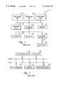
- FIG. 1 illustrates a conventional computer system 10 using some of the foregoing buses.
- Computer system 10 has several processing units (CPUs) 12 a , 12 b , and 12 c which are connected, via a system bus 14 , to a system memory device 16 (random-access memory or RAM) that is used by the processing units to carry out program instructions, and firmware 18 whose primary purpose is to seek out and load an operating system from a peripheral device (usually the permanent memory device or hard disk) whenever the computer is first turned on.
- the processing units are connected to various peripheral devices via a PCI host bridge 20 .
- These peripheral devices comprise PCI devices 22 and 24 connected to the PCI bus 26 , and an ISA device 28 connected to an ISA bus 30 which is connected to an ISA bridge 32 .
- These input/output (I/O) devices may include, for example, a display monitor, keyboard, graphical pointer device (mouse), a permanent storage device (direct access storage device or DASD), etc.
- I 2 C bus Another widely recognized bus design used for microelectronics is known as the I 2 C bus.
- the term “I 2 C” is an abbreviation for “inter-IC,” referring to communications between two or more integrated circuits.
- the bus physically consists of two active wires and a ground connection.
- the active wires (data and clock) are both bidirectional.
- An exemplary configuration using an I 2 C bus is shown in FIG. 2 .
- Two microcontrollers 34 and 36 are connected to the clock and data lines, along with various other circuits such as a liquid crystal display (LCD) driver 38 , a memory unit 40 , and a data converter 42 .
- LCD liquid crystal display
- the I 2 C protocol supports multiple “masters,” meaning that multiple chips can be interconnected to the same bus and each one can act as a master.
- the IC that initiates a given data transfer on the bus is considered the bus master.
- all the other devices are regarded as “slaves.” Every component connected to the bus has its own unique address, which is used to indicate a target for data.
- Each of these chips can act as a receiver or transmitter depending on its intended functionality.
- the I 2 C bus design is used in many microcontroller-based applications for control, diagnostics or power management, and is especially useful in video devices such as computer monitors, televisions and VCRs.
- This design was originally created to provide an easy way to connect a CPU to peripheral chips in a television set, and is still commonly used to connect computer systems to peripheral devices.
- some versions of the PowerPCTM processor sold by International Business Machines Corp. (IBM—assignee of the present invention) are provided with an I 2 C port to offer an alternative communications path for selected peripherals.
- IBM's NetfinityTM rack server system uses such a service processor to allow I 2 C communications with I/O subsystems.
- the service processor communicates with all I/O planars using the I 2 C bus to access information like vital product data (VPD) codes, planar voltages, temperatures, etc.
- VPD vital product data
- the I/O planars are located in the rack on a base I/O drawer and one or more expansion I/O drawers.
- I/O planars can use an I/O expander to select one of several I 2 C channels of the I/O subsystem.
- One example is the PCF8574 remote 8-bit I/O expander.
- the PCF8574 is a complementary metal-oxide semiconducting (CMOS) circuit that provides general purpose remote I/O expansion for most microcontroller families via an I 2 C bus.
- CMOS complementary metal-oxide semiconducting
- the device has an interrupt line which can be directly connected to the interrupt logic of a microcontroller. By sending an interrupt signal on this line, the remote I/O planar can inform the microcontroller if there is incoming data on its ports without having to communicate via the I 2 C bus, so the PCF8574 can remain a simple slave device.
- I 2 C I/O expander addresses of all I/O planars, to different addresses.
- this configuration is performed manually, such as by using jumpers to interconnect address pins on the expanders, or using cables attached to the drawer frame providing an individual address.
- logic components such as processors, microcontrollers and input/output (I/O) devices.
- a method of configuring a data communications system generally comprising the steps of connecting a first logic component to a first communications bus, connecting a second logic component to the first communications bus wherein the second logic component has a default communications address, connecting a third logic component to a second communications bus, changing the default communications address of the second logic component to a first assigned address, and connecting the second logic component to the second communications bus in response to the changing step.
- the second logic component may include a multiplexer having an input connected to the first communications bus, and a plurality of outputs, a first one of the outputs being connected to an input/output device, and a second one of the outputs being connected to the second communications bus, the second output being disabled when the second logic component has the default communications address; the second logic component is connected to the second communications bus by enabling the second output of the multiplexer.
- the address can be changed by having the first logic component write the first assigned address to the second logic component.
- the invention may comprise the further steps of connecting a fourth logic component to a third communications bus, changing the default communications address of the third logic component to a second assigned address, after the connecting of the second logic component to the second communications bus, and then connecting the third logic component to the third communications bus in response to the changing of the default communications address of the third logic component to the second assigned address.
- the first logic component can communicate with the second and third logic components using an I 2 C bus protocol to send data across the first and second communications buses.
- the invention is particularly adapted for use with a computer system, wherein the first logic component is a service processor of the computer system, the service processor having an I 2 C port connected to the first communications bus, and one or more peripheral devices are also connected to the service processor using an alternate communications path, e.g., a system bus.
- the service processor communicates with the second logic component using an I 2 C bus protocol to send data across the first communications bus to an input/output expander of the second logic component.
- the input/output expander has a plurality of ports, all of which can initially be set as input ports.
- FIG. 1 is a block diagram of a conventional computer system having several communications buses, including a system bus, and peripheral component interconnect bus, and an expansion bus;
- FIG. 2 is a block diagram of a prior art interintegrated circuit (I 2 C) communications bus used to interconnect various logical devices; and
- FIG. 3 is a schematic diagram of a portion of a data processing system constructed in accordance with the present invention, having a service processor communicating with a plurality of input/output expanders using I 2 C buses.
- I/O subsystem 50 is generally comprised of a service processor 52 and a plurality of I/O planars, including a first I/O planar 54 in a base I/O drawer, and a second I/O planar 56 in an expansion I/O drawer. Although only two I/O planars are shown, additional expansion drawers may be provided to add even more I/O planars, as further discussed below.
- Service processor 52 may be a PowerPCTM processor having an I 2 C port providing a communications path for I/O devices such as modems, LAN adapters, permanent storage devices, televisions, etc.
- the data processing system may have multiple processors, and more than one processor can be provided with an I 2 C port, i.e., the data processing system can have multiple I/O subsystems.
- Other conventional computer components can be provided for the data processing system via communications buses (not shown), such as a peripheral component interconnect (PCI) bus.
- PCI peripheral component interconnect
- Service processor 52 communicates with the I/O planars using I 2 C buses, including a first I 2 C bus 58 connected to an I/O expander 60 (such as the PCF8574AT remote 8-bit I/O expander) of I/O planar 54 .
- I/O expander 60 is further connected to a logic circuit 62 (Quality Semiconductor's QS3253 chip) which acts as a 4:1 FET switch multiplexer/demultiplexer.
- the address of I/O expander 60 can be set to 42 through 4E hexadecimal (even addresses only), determined by its address pins A 2 , A 1 and A 0 .
- I/O expander 60 converts the I 2 C serial data sent from service processor 52 to 8-bit output port data.
- port bits P 3 , P 2 and P 1 are connected, respectively, to three D-latch pins D 2 , D 1 and D 0 . These latches are used to store the signals of A 2 , A 1 and A 0 .
- the fourth D-latch, D 3 is used to allow the address bits to be latched only once after reset. Signals are latched when I 2 C bus 58 is in the stop phase to prevent the data output from interfering with the current I 2 C operation. This design allows service processor 52 to write new I/O planar address bits only once until the next reset.
- Multiplexer/demultiplexer 62 uses pins S 0 and S 1 (also latched at the I 2 C stop phase) to select one of the four output I 2 C buses 64 , 66 , 68 , and 70 to connect to the input I 2 C bus 58 .
- the EA# and EB# pins of logic circuit 62 when low, enable the connections of signal group A and signal group B, respectively.
- the top three output I 2 C buses 64 , 66 and 68 can be used to access I 2 C devices related to the base I/O drawer.
- the fourth I 2 C bus 70 is connected to the input of the next I/O planar 56 , that is, to another I/O expander 72 on I/O planar 56 .
- I/O planar 56 has the same general design as I/O planar 54 , and is able to connect to a further I 2 C bus 74 via another multiplexer/demultiplexer 76 .
- This embodiment can thus support up to seven I/O planars with respective hex addresses of 42, 44, 46, 48, 4A, 4C and 4E (address 4D is reserved for use with the first logic component, i.e., service processor 52 ).
- reset e.g., power-on reset
- all D-latch outputs are set active/high (1's), so the addresses of all of the I/O expanders (including I/O expanders 60 and 72 ) are initialized to 4E.
- the EA# and EB# pins of each QS3253 chip are also set active/high so, initially, no output I 2 C signals are connected to the input I 2 C signals.
- the following software procedure is used to set the appropriate addresses.
- the base I/O drawer I 2 C address is initially 4E.
- the outputs of multiplexer/demultiplexer 62 are disabled (using tri-state logic), so service processor I 2 C bus 58 cannot yet reach the other drawers.
- Service processor 52 then writes to address 4E with data “1111 — 0010” to change the base I/O drawer address to 42 and enable multiplexer/demultiplexer 62 to connect to the first expansion I/O drawer (I/O planar 56 ).
- the base I/O drawer has the I 2 C address of 42, while the first expansion I/O drawer has the I 2 C address of 4E.
- Service processor 52 then writes again to address 4E, but this time with data “1111 — 0100” to assign I 2 C address 44 to the first expansion I/O drawer, and enable multiplexer/demultiplexer 76 to connect to the I 2 C bus for the next expansion I/O drawer.
- These steps are repeated with different data being sent by service processor 52 to I 2 C address 4E, until each of the remaining expansion I/O drawer addresses are configured to the other available values.
- the present invention thus configures the new I 2 C addresses automatically, and without any extra hardware or manual intervention.
- the I/O planars can also be made responsive to a reset signal generated by service processor 52 .
- the service processor can dynamically reconfigure the I/O subsystem, such as when a new I/O planar is added in another expansion I/O drawer.
Abstract
Description
Claims (19)
Priority Applications (1)
| Application Number | Priority Date | Filing Date | Title |
|---|---|---|---|
| US09/281,083 US6438624B1 (en) | 1999-03-30 | 1999-03-30 | Configurable I/O expander addressing for I/O drawers in a multi-drawer rack server system |
Applications Claiming Priority (1)
| Application Number | Priority Date | Filing Date | Title |
|---|---|---|---|
| US09/281,083 US6438624B1 (en) | 1999-03-30 | 1999-03-30 | Configurable I/O expander addressing for I/O drawers in a multi-drawer rack server system |
Publications (1)
| Publication Number | Publication Date |
|---|---|
| US6438624B1 true US6438624B1 (en) | 2002-08-20 |
Family
ID=23075883
Family Applications (1)
| Application Number | Title | Priority Date | Filing Date |
|---|---|---|---|
| US09/281,083 Expired - Lifetime US6438624B1 (en) | 1999-03-30 | 1999-03-30 | Configurable I/O expander addressing for I/O drawers in a multi-drawer rack server system |
Country Status (1)
| Country | Link |
|---|---|
| US (1) | US6438624B1 (en) |
Cited By (12)
| Publication number | Priority date | Publication date | Assignee | Title |
|---|---|---|---|---|
| US6510481B1 (en) * | 1999-11-01 | 2003-01-21 | Lsi Logic Corporation | Method for out-of-band network communication |
| US20030018823A1 (en) * | 2001-07-18 | 2003-01-23 | Roberto Ponticelli | Network enabled low-cost smart microdevice |
| US20030135679A1 (en) * | 2002-01-16 | 2003-07-17 | Tangen Wayne A. | Circuit and method for expanding a serial bus |
| US20030212847A1 (en) * | 2002-05-09 | 2003-11-13 | International Business Machines Corporation | Apparatus for supporting I2C bus masters on a secondary side of an I2C multiplexor |
| US6961785B1 (en) * | 2000-08-03 | 2005-11-01 | International Business Machines Corporation | Permanent open firmware PCI host bridge (PHB) unit addressing to support dynamic memory mapping and swapping of I/O drawers |
| US20050289273A1 (en) * | 2004-06-25 | 2005-12-29 | Lee Bong-Geun | Communication apparatus using inter integrated circuit bus and communication method thereof |
| US20060117124A1 (en) * | 2004-11-30 | 2006-06-01 | Grasso Lawrence J | Multiple host support for remote expansion apparatus |
| WO2006117748A1 (en) * | 2005-04-29 | 2006-11-09 | Koninklijke Philips Electronics, N.V. | Slave device with latched request for service |
| US20080155368A1 (en) * | 2006-10-10 | 2008-06-26 | Bofferding Nicholas E | Dynamically updating alias location codes with correct location codes during concurrent installation of a component in a computer system |
| CN105426331A (en) * | 2015-11-13 | 2016-03-23 | 上海斐讯数据通信技术有限公司 | PHY chip management system and PHY chip management method |
| DE102015214133A1 (en) * | 2015-07-27 | 2017-02-02 | Continental Automotive Gmbh | Integrated circuit for operating on a bus and method for operating the integrated circuit |
| US11106618B2 (en) * | 2019-06-26 | 2021-08-31 | STMicroelectronics (Alps) SAS | Method for addressing an integrated circuit on a bus and corresponding device |
Citations (4)
| Publication number | Priority date | Publication date | Assignee | Title |
|---|---|---|---|---|
| US5623610A (en) * | 1994-10-31 | 1997-04-22 | Intel Corporation | System for assigning geographical addresses in a hierarchical serial bus by enabling upstream port and selectively enabling disabled ports at power on/reset |
| US5664221A (en) * | 1995-11-14 | 1997-09-02 | Digital Equipment Corporation | System for reconfiguring addresses of SCSI devices via a device address bus independent of the SCSI bus |
| US5805927A (en) * | 1994-01-28 | 1998-09-08 | Apple Computer, Inc. | Direct memory access channel architecture and method for reception of network information |
| US5926648A (en) * | 1996-08-22 | 1999-07-20 | Zilog, Inc. | I/O port and RAM memory addressing technique |
-
1999
- 1999-03-30 US US09/281,083 patent/US6438624B1/en not_active Expired - Lifetime
Patent Citations (4)
| Publication number | Priority date | Publication date | Assignee | Title |
|---|---|---|---|---|
| US5805927A (en) * | 1994-01-28 | 1998-09-08 | Apple Computer, Inc. | Direct memory access channel architecture and method for reception of network information |
| US5623610A (en) * | 1994-10-31 | 1997-04-22 | Intel Corporation | System for assigning geographical addresses in a hierarchical serial bus by enabling upstream port and selectively enabling disabled ports at power on/reset |
| US5664221A (en) * | 1995-11-14 | 1997-09-02 | Digital Equipment Corporation | System for reconfiguring addresses of SCSI devices via a device address bus independent of the SCSI bus |
| US5926648A (en) * | 1996-08-22 | 1999-07-20 | Zilog, Inc. | I/O port and RAM memory addressing technique |
Cited By (22)
| Publication number | Priority date | Publication date | Assignee | Title |
|---|---|---|---|---|
| US6510481B1 (en) * | 1999-11-01 | 2003-01-21 | Lsi Logic Corporation | Method for out-of-band network communication |
| US6782437B2 (en) * | 1999-11-01 | 2004-08-24 | Lsi Logic Corporation | Method of communicating on a network |
| US6961785B1 (en) * | 2000-08-03 | 2005-11-01 | International Business Machines Corporation | Permanent open firmware PCI host bridge (PHB) unit addressing to support dynamic memory mapping and swapping of I/O drawers |
| US20030018823A1 (en) * | 2001-07-18 | 2003-01-23 | Roberto Ponticelli | Network enabled low-cost smart microdevice |
| US6874050B2 (en) * | 2002-01-16 | 2005-03-29 | Hewlett-Packard Development Company, L.P. | Circuit and method for expanding a serial bus |
| US20030135679A1 (en) * | 2002-01-16 | 2003-07-17 | Tangen Wayne A. | Circuit and method for expanding a serial bus |
| US20030212847A1 (en) * | 2002-05-09 | 2003-11-13 | International Business Machines Corporation | Apparatus for supporting I2C bus masters on a secondary side of an I2C multiplexor |
| US6816939B2 (en) * | 2002-05-09 | 2004-11-09 | International Business Machines Corporation | Apparatus for supporting I2C bus masters on a secondary side of an I2C multiplexor |
| US20050289273A1 (en) * | 2004-06-25 | 2005-12-29 | Lee Bong-Geun | Communication apparatus using inter integrated circuit bus and communication method thereof |
| US20060117124A1 (en) * | 2004-11-30 | 2006-06-01 | Grasso Lawrence J | Multiple host support for remote expansion apparatus |
| US8484398B2 (en) * | 2004-11-30 | 2013-07-09 | International Business Machines Corporation | Multiple host support for remote expansion apparatus |
| US20070283070A1 (en) * | 2004-11-30 | 2007-12-06 | Grasso Lawrence J | Multiple Host Support For Remote Expansion Apparatus |
| US8984202B2 (en) | 2004-11-30 | 2015-03-17 | Lenovo Enterprise Solutions (Singapore) Pte. Ltd. | Multiple host support for remote expansion apparatus |
| WO2006117748A1 (en) * | 2005-04-29 | 2006-11-09 | Koninklijke Philips Electronics, N.V. | Slave device with latched request for service |
| US7761637B2 (en) | 2005-04-29 | 2010-07-20 | Nxp B.V. | Slave device with latched request for service |
| US20080215779A1 (en) * | 2005-04-29 | 2008-09-04 | Nxp B.V. | Slave Device with Latched Request for Service |
| US8001287B2 (en) * | 2006-10-10 | 2011-08-16 | International Business Machines Corporation | Dynamically updating alias location codes with correct location codes during concurrent installation of a component in a computer system |
| US20080155368A1 (en) * | 2006-10-10 | 2008-06-26 | Bofferding Nicholas E | Dynamically updating alias location codes with correct location codes during concurrent installation of a component in a computer system |
| DE102015214133A1 (en) * | 2015-07-27 | 2017-02-02 | Continental Automotive Gmbh | Integrated circuit for operating on a bus and method for operating the integrated circuit |
| US10394748B2 (en) | 2015-07-27 | 2019-08-27 | Cpt Group Gmbh | Integrated circuit for operating on a bus, and method for operating the integrated circuit |
| CN105426331A (en) * | 2015-11-13 | 2016-03-23 | 上海斐讯数据通信技术有限公司 | PHY chip management system and PHY chip management method |
| US11106618B2 (en) * | 2019-06-26 | 2021-08-31 | STMicroelectronics (Alps) SAS | Method for addressing an integrated circuit on a bus and corresponding device |
Similar Documents
| Publication | Publication Date | Title |
|---|---|---|
| US5835784A (en) | System for booting processor from remote memory by preventing host processor from configuring an environment of processor while configuring an interface unit between processor and remote memory | |
| US5860021A (en) | Single chip microcontroller having down-loadable memory organization supporting "shadow" personality, optimized for bi-directional data transfers over a communication channel | |
| US6185642B1 (en) | Bus for high frequency operation with backward compatibility and hot-plug ability | |
| US6256700B1 (en) | Bus/port switching system and method for a computer | |
| JP3838278B2 (en) | Bridge circuit between two buses of a computer system | |
| US7085863B2 (en) | I2C device including bus switches and programmable address | |
| US6295568B1 (en) | Method and system for supporting multiple local buses operating at different frequencies | |
| US5613074A (en) | Automatic disabling of SCSI bus terminators | |
| US6035355A (en) | PCI system and adapter requirements following reset | |
| JP3232283B2 (en) | Computer system supporting PCI bus | |
| US6772263B1 (en) | PCI arbiter with hot plug controller support | |
| US20070073959A1 (en) | Dynamic reconfiguration of PCI express links | |
| US6438624B1 (en) | Configurable I/O expander addressing for I/O drawers in a multi-drawer rack server system | |
| EP1358564B1 (en) | System having i2c self bus switching devices | |
| US6922194B2 (en) | Method and apparatus for maintaining load balance on a graphics bus when an upgrade device is installed | |
| US20080144649A1 (en) | Apparatus for multiplexing signals through I/O pins | |
| EP0836141B1 (en) | A fault-tolerant bus system | |
| US6510485B1 (en) | Stabilizing circuit for interfacing device | |
| WO2000034878A1 (en) | Programmable pull-up for a universal serial bus interface | |
| JPH11175208A (en) | System and method for electrically disconnecting device from device at higher voltage | |
| US6919878B2 (en) | Keyboard/mouse switching controller | |
| KR100464989B1 (en) | Control bus system and bus arbitration method | |
| US6678287B1 (en) | Method for multiplexing signals through I/O pins | |
| US20240119019A1 (en) | Sharing communication lines among multiple buses | |
| US20040177204A1 (en) | Bus interface with variable resistance coupling |
Legal Events
| Date | Code | Title | Description |
|---|---|---|---|
| AS | Assignment |
Owner name: INTERNATIONAL BUSINESS MACHINES CORPORATION, NEW Y Free format text: ASSIGNMENT OF ASSIGNORS INTEREST;ASSIGNORS:KU, YI-MING;TUTEN, WALLACE G.;REEL/FRAME:009864/0570 Effective date: 19990329 |
|
| STCF | Information on status: patent grant |
Free format text: PATENTED CASE |
|
| AS | Assignment |
Owner name: LENOVO (SINGAPORE) PTE LTD.,SINGAPORE Free format text: ASSIGNMENT OF ASSIGNORS INTEREST;ASSIGNOR:INTERNATIONAL BUSINESS MACHINES CORPORATION;REEL/FRAME:016891/0507 Effective date: 20050520 Owner name: LENOVO (SINGAPORE) PTE LTD., SINGAPORE Free format text: ASSIGNMENT OF ASSIGNORS INTEREST;ASSIGNOR:INTERNATIONAL BUSINESS MACHINES CORPORATION;REEL/FRAME:016891/0507 Effective date: 20050520 |
|
| REMI | Maintenance fee reminder mailed | ||
| FPAY | Fee payment |
Year of fee payment: 4 |
|
| SULP | Surcharge for late payment | ||
| FPAY | Fee payment |
Year of fee payment: 8 |
|
| FPAY | Fee payment |
Year of fee payment: 12 |
|
| AS | Assignment |
Owner name: LENOVO PC INTERNATIONAL, HONG KONG Free format text: NUNC PRO TUNC ASSIGNMENT;ASSIGNOR:LENOVO (SINGAPORE) PTE LTD.;REEL/FRAME:037160/0001 Effective date: 20130401 |