US6426662B1 - Twisted-ring oscillator and delay line generating multiple phases using differential dividers and comparators to match delays - Google Patents
Twisted-ring oscillator and delay line generating multiple phases using differential dividers and comparators to match delays Download PDFInfo
- Publication number
- US6426662B1 US6426662B1 US09/683,040 US68304001A US6426662B1 US 6426662 B1 US6426662 B1 US 6426662B1 US 68304001 A US68304001 A US 68304001A US 6426662 B1 US6426662 B1 US 6426662B1
- Authority
- US
- United States
- Prior art keywords
- delay
- output
- clock
- true
- complement
- Prior art date
- Legal status (The legal status is an assumption and is not a legal conclusion. Google has not performed a legal analysis and makes no representation as to the accuracy of the status listed.)
- Expired - Fee Related
Links
Images


Classifications
-
- H—ELECTRICITY
- H03—ELECTRONIC CIRCUITRY
- H03K—PULSE TECHNIQUE
- H03K3/00—Circuits for generating electric pulses; Monostable, bistable or multistable circuits
- H03K3/02—Generators characterised by the type of circuit or by the means used for producing pulses
- H03K3/027—Generators characterised by the type of circuit or by the means used for producing pulses by the use of logic circuits, with internal or external positive feedback
- H03K3/03—Astable circuits
-
- H—ELECTRICITY
- H03—ELECTRONIC CIRCUITRY
- H03K—PULSE TECHNIQUE
- H03K3/00—Circuits for generating electric pulses; Monostable, bistable or multistable circuits
- H03K3/02—Generators characterised by the type of circuit or by the means used for producing pulses
- H03K3/023—Generators characterised by the type of circuit or by the means used for producing pulses by the use of differential amplifiers or comparators, with internal or external positive feedback
- H03K3/0231—Astable circuits
-
- H—ELECTRICITY
- H03—ELECTRONIC CIRCUITRY
- H03K—PULSE TECHNIQUE
- H03K3/00—Circuits for generating electric pulses; Monostable, bistable or multistable circuits
- H03K3/02—Generators characterised by the type of circuit or by the means used for producing pulses
- H03K3/027—Generators characterised by the type of circuit or by the means used for producing pulses by the use of logic circuits, with internal or external positive feedback
- H03K3/03—Astable circuits
- H03K3/0315—Ring oscillators
- H03K3/0322—Ring oscillators with differential cells
-
- H—ELECTRICITY
- H03—ELECTRONIC CIRCUITRY
- H03K—PULSE TECHNIQUE
- H03K5/00—Manipulating of pulses not covered by one of the other main groups of this subclass
- H03K5/13—Arrangements having a single output and transforming input signals into pulses delivered at desired time intervals
- H03K5/133—Arrangements having a single output and transforming input signals into pulses delivered at desired time intervals using a chain of active delay devices
-
- H—ELECTRICITY
- H03—ELECTRONIC CIRCUITRY
- H03L—AUTOMATIC CONTROL, STARTING, SYNCHRONISATION, OR STABILISATION OF GENERATORS OF ELECTRONIC OSCILLATIONS OR PULSES
- H03L7/00—Automatic control of frequency or phase; Synchronisation
- H03L7/06—Automatic control of frequency or phase; Synchronisation using a reference signal applied to a frequency- or phase-locked loop
- H03L7/08—Details of the phase-locked loop
- H03L7/081—Details of the phase-locked loop provided with an additional controlled phase shifter
- H03L7/0812—Details of the phase-locked loop provided with an additional controlled phase shifter and where no voltage or current controlled oscillator is used
- H03L7/0816—Details of the phase-locked loop provided with an additional controlled phase shifter and where no voltage or current controlled oscillator is used the controlled phase shifter and the frequency- or phase-detection arrangement being connected to a common input
-
- H—ELECTRICITY
- H03—ELECTRONIC CIRCUITRY
- H03L—AUTOMATIC CONTROL, STARTING, SYNCHRONISATION, OR STABILISATION OF GENERATORS OF ELECTRONIC OSCILLATIONS OR PULSES
- H03L7/00—Automatic control of frequency or phase; Synchronisation
- H03L7/06—Automatic control of frequency or phase; Synchronisation using a reference signal applied to a frequency- or phase-locked loop
- H03L7/08—Details of the phase-locked loop
- H03L7/099—Details of the phase-locked loop concerning mainly the controlled oscillator of the loop
- H03L7/0995—Details of the phase-locked loop concerning mainly the controlled oscillator of the loop the oscillator comprising a ring oscillator
-
- H—ELECTRICITY
- H03—ELECTRONIC CIRCUITRY
- H03K—PULSE TECHNIQUE
- H03K5/00—Manipulating of pulses not covered by one of the other main groups of this subclass
- H03K2005/00013—Delay, i.e. output pulse is delayed after input pulse and pulse length of output pulse is dependent on pulse length of input pulse
- H03K2005/00078—Fixed delay
- H03K2005/00097—Avoiding variations of delay using feedback, e.g. controlled by a PLL
Definitions
- This invention relates to clock generators, and more particularly to precision multi-phase clock generators using differential logic.
- clock logic Many electronic devices and systems employ clock logic. High-speed clocks can be routed to flip-flops and registers to control sequencing of logical states and signals. Very precise clocks are required for some applications. In particular, multiple phases of a clock can be generated, allowing very precise selection of the clock's phase.
- FIG. 1 shows a prior-art clock generator that uses a ring oscillator to generate 16 clock phases.
- a ring of 16 inverters 12 passes a clock pulse around in a loop.
- Each inverter 12 in the loop outputs a clock with a phase shift that depends on the position of the inverter within the loop.
- the first inverter 12 outputs clock ⁇ 1 with a phase being ahead of clock ⁇ 5 by four inverter delays and ahead of clock ⁇ 9 by eight inverter delays.
- a clock period can be divided into 16 equally-spaced phases ⁇ 1 to ⁇ 16.
- Erratic oscillation or multi-frequency oscillation can occur when 8 or more inverter stages are used in a loop. For example, when each of 8 inverter stages has one pole and a 90-degree phase shift, the total phase shift in the loop is 8 ⁇ 90 or 720 degrees. Then the loop can oscillate at either or both 720 degrees and 360 degrees. Such multiple oscillation can produce frequency overtones in the outputs. This is similar to a vibrating string on a musical instrument, which can vibrate at secondary frequencies or overtones.
- FIG. 1 shows a prior-art clock generator that uses a ring oscillator to generate 16 clock phases.
- FIG. 2 is a block diagram of twisted-ring clock generator using differential logic.
- FIGS. 3A-3C are waveforms highlighting operation of the clock generator of FIG.
- FIG. 4 is a schematic of a differential toggle flip-flop.
- FIG. 5 is a schematic of a differential-to-single-ended buffer.
- FIG. 6 is a schematic of the delay stages operating in a voltage-controlled oscillator (VCO).
- VCO voltage-controlled oscillator
- FIG. 7 shows the use of the differential delay stages as a VCO in a PLL.
- FIG. 8 shows the use of the differential delay stages as an open-ended delay line in a delay-locked loop (DLL).
- DLL delay-locked loop
- FIG. 9 is an alternative embodiment of the twisted-ring oscillator using differential toggle flip-flops.
- the present invention relates to an improvement in clock generators.
- the following description is presented to enable one of ordinary skill in the art to make and use the invention as provided in the context of a particular application and its requirements.
- Various modifications to the preferred embodiment will be apparent to those with skill in the art, and the general principles defined herein may be applied to other embodiments. Therefore, the present invention is not intended to be limited to the particular embodiments shown and described, but is to be accorded the widest scope consistent with the principles and novel features herein disclosed.
- FIG. 2 is a block diagram of twisted-ring clock generator using differential logic. To avoid multiple-frequency oscillation, the number of stages is reduced to less than 8, such as four.
- the delay stages 14 A- 14 D are differential buffers that have true (+) and complement ( ⁇ ) inputs, and drive true (+) and complement ( ⁇ ) outputs. When the true input has a higher voltage than the complement input, the true output is driven to a higher voltage than the complement output for any delay stage.
- the true output from delay stage 14 A is connected to the true input of delay stage 14 B, while the complement output from delay stage 14 A is connected to the complement input of delay stage 14 B.
- true outputs of delays stages 14 B, 14 C are connected to true inputs of delay stages 14 C, 14 D, while the complement outputs are connected to complement inputs for these stages.
- the true and complement outputs of last delay stage 14 D are crossed over, so that the true output from last delay stage 14 D drives the complement input of first delay stage 14 A, while the complement output of delay stage 14 D drives the true input of delay stage 14 A.
- This cross-over of the final stage's outputs effectively produces a loop of twice as many total delay stages as a signal passes around the loop twice.
- a rising-edge pulse from first delay stage 14 A passes along signals DEL 1 , DEL 2 , DEL 3 , DEL 4 , then loops back and crosses over to DEL 1 B, DEL 2 B, DEL 3 B, and finally DEL 1 B.
- Differential toggle flip-flops 20 - 27 are connected to the true and complement outputs of delay stages 14 A- 14 D.
- the differential clock inputs CK+ and CK ⁇ of a differential toggle flip-flop are connected to the true and complement outputs of a delay stage.
- Toggle flip-flops have their Q-BAR output connected back to their D input, so that they change (toggle) state on each rising edge of the clock. Since the flip-flops are fully differential, the Q+ output is fed back to the D ⁇ input, and the Q ⁇ output is fed back to the D+ input of each differential toggle flip-flop 20 - 27 .
- Each delay stage has a pair of differential toggle flip-flops connected in a complementary fashion. One flip-flop changes state on the rising edge of the true output, while the other flip-flop changes state on the rising edge of the complement output.
- delay stage 14 A has differential toggle flip-flop 20 that changes on the rising edge of CK+, and has input CK+ connected to true output DEL 1 , and input CK ⁇ connected to complement output DEL 1 B.
- Delay stage 14 A also has a second differential toggle flip-flop 24 that changes on the rising edge of CK ⁇ , which is also the falling edge of CK+, and has input CK ⁇ connected to true output DEL 1 , and input CK+ connected to complement output DEL 1 B.
- the input frequency of delay stages 14 A- 14 D is divided by two by differential toggle flip-flops 20 - 27 . Since each of the pair of toggle flip-flops on a delay stage change with different clock edges (one rising edge, one falling edge), the outputs of the two differential toggle flip-flops for a delay stage are delayed in phase from each other by half a clock period.
- differential toggle flip-flops 20 - 27 are coupled to differential-to-single-ended buffers 30 .
- These buffers 30 can be simple op amps, comparators, or other buffers with a pair of differential inputs and a single output. When the + input of a buffer 30 is higher in voltage than its ⁇ input, the output of buffer 30 is high; otherwise the output is low.
- a pair of buffers 30 produce a true and a complement output for each differential toggle flip-flop 20 - 27 .
- Each of the 16 buffers 30 produces a different one of the 16 phases of the output clock ⁇ 1- ⁇ 16.
- FIGS. 3A-3C are waveforms highlighting operation of the clock generator of FIG. 2 .
- FIG. 3A shows the outputs of the four delay stages 14 A- 14 D. A rising clock edge propagates around the loop, first appearing on the true output (DEL 1 ) of first delay stage 14 A, then the true output (DEL 2 ) of second delay stage 14 B, then DEL 3 of the third stage 14 C, and the DEL 4 output of last delay stage 14 D.
- the true output DEL 4 of last delay stage 14 D is then crossed over and fed back to the complement input of first delay stage 14 A, which outputs a rising edge of its complement output DEL 1 B.
- This rising clock edge on the complement outputs then propagates around the loop, next appearing on the complement output (DEL 2 B) of second delay stage 14 B, then DEL 3 B of the third stage 14 C, and the DEL 4 B output of last delay stage 14 D.
- the complement output DEL 4 B of the last delay stage 14 D then crosses over and is fed back to the true input of first delay stage 14 A, which again drives its true output DEL 1 with a rising edge.
- the rising edge signal continues to propagate around the loop, producing oscillating outputs at a frequency corresponding to the total loop delay, or 8 stages of delay.
- FIG. 3B highlights generation of four clock phases from the output of one delay stage.
- the true output DEL 1 of first delay stage 14 A and the complement output DEL 1 B change in opposite directions since they are both driven by the same differential delay stage 14 A.
- Differential toggle flip-flop 20 has its CK+ input connected to DEL 1 , and its CK ⁇ input connected to DEL 1 B. Since the differential toggle flip-flop changes on the rising edge of its positive clock input (CK+), the outputs of differential toggle flip-flop 20 change state in response to the rising edge of CK+ (DEL 1 ) and falling edge of CK ⁇ (DEL 1 B). Since differential toggle flip-flop 20 is fully differential, its outputs Q+, Q ⁇ have identical delays from the clock input (DEL 1 , DEL 1 B).
- the differential outputs Q+, Q ⁇ of differential toggle flip-flop 20 drive a pair of buffers 30 , which convert the differential outputs to standard single-ended logic signals.
- One buffer 30 has its + input driven by Q+, while its ⁇ input driven by Q ⁇ , and it produces clock ⁇ 1.
- the other buffer 30 has its ⁇ input driven by Q+, while its + input driven by Q ⁇ , and it produces the inverse of clock ⁇ 1, which is ⁇ 9.
- the ⁇ 1 and ⁇ 9 differential-input-to-rising-edge-output delays are identical regardless of the input polarity connection, since the delays are defined by crossing points and not levels. No systematic error exists, only random mismatch. Therefore, the output rising edges of buffers 30 preserve the ideal timing relationships at their differential inputs.
- the other differential toggle flip-flop 24 has its CK+ input connected to DEL 1 B, and its CK ⁇ input connected to DEL 1 . Since the differential toggle flip-flop changes on the rising edge of its positive clock input (CK+) when both inputs CK+, CK ⁇ switch, the outputs of differential toggle flip-flop 20 change state in response to the crossover of the rising edge of CK+ (DEL 1 B) and falling edge of CK ⁇ (DEL 1 ). This is the other clock edge of DEL 1 , DEL 1 B.
- the differential outputs Q+, Q ⁇ of differential toggle flip-flop 24 also drive another pair of buffers 30 , which convert the differential outputs to standard single-ended logic signals.
- One buffer 30 has its + input driven by Q+, while its ⁇ input driven by Q ⁇ , and it produces clock ⁇ 5.
- the other buffer 30 has its ⁇ input driven by Q+, while its + input driven by Q ⁇ , and it produces the inverse of clock ⁇ 5, which is ⁇ 13.
- FIG. 3C shows the 16 output clocks ⁇ 1- ⁇ 16 that are generated from the four differential delay stages 14 A- 14 D, differential toggle flip-flops 20 - 27 , and buffers 30 . Since the toggle flip-flops divide the frequency of delay signals DEL 1 - 4 by two, the frequency of these output clocks ⁇ 1- ⁇ 16 are half the frequency of signal DEL 1 . The phases of clocks ⁇ 1- ⁇ 16 are equally spaced by one-sixteenth of the output clock period over two periods of the input clock DEL 1 . Although there is a delay from DEL 1 to the output clocks ⁇ 1- ⁇ 16, the delays among the output clocks are closely matched. Very precise multi-phase clocks result.
- FIG. 4 is a schematic of a differential toggle flip-flop.
- Differential toggle flip-flop 20 receives a clock (CK+) and clock-bar (CK ⁇ ) input from the true and complement outputs from a delay stage, such as DEL 1 , DEL 1 B from first delay stage 14 A.
- Differential toggle flip-flop 24 reverses the connection of DEL 1 and DEL 1 B to CK ⁇ , CK+.
- Other flip-flops 21 - 23 , 25 - 27 take inputs from DEL 1 -DEL 4 and DEL 2 B-DEL 4 B.
- the Q+ (QFF+) and Q ⁇ (QFF ⁇ ) outputs from the slave portion of the flip-flop are crossed over and fed back to the data inputs D ⁇ , D+, which are the gates of n-channel transistors 64 , 66 in the master portion of the flip-flop. This causes the differential flip-flop to operate as a toggle or divide-by-two flip-flop. Each rising edge of the CK+ clock causes the output to toggle state.
- the clock inputs CK+, CK ⁇ are applied to the gates of n-channel source-follower transistors 52 , 50 .
- Tail n-channel transistors 56 , 54 sink current from source-follower transistors 52 , 50 , respectively.
- the voltages of CK+, CK ⁇ are modulated, the voltages of clock nodes C 1 , C 2 are also modulated.
- the master portion sinks a current through tail transistor 58 .
- Current is steered from node G 3 to node G 4 as CK+ rises and CK ⁇ falls. This causes the data applied to the gates of n-channel transistors 64 , 66 to be transferred and stored on nodes G 5 , G 6 by virtue of the feedback of nodes G 5 , G 6 to the gates of master storage transistors 70 , 72 .
- Resistors 67 , 68 supply current to master storage nodes G 6 , G 5 .
- the slave portion sinks a current through tail transistor 78 .
- Clock nodes C 1 , C 2 are applied to the gates of clock transistors 82 , 80 , respectively.
- Current is steered from node G 8 to node G 7 as CK ⁇ rises and CK+ falls.
- This causes the data applied to the gates of n-channel transistors 74 , 76 to be transferred and stored on nodes QFF+, QFF ⁇ by virtue of the feedback of nodes QFF+, QFF ⁇ to the gates of slave storage transistors 86 , 84 .
- Resistors 88 , 87 supply current to master storage nodes QFF+, QFF ⁇ .
- the slave portion latches data on CK+ falling, while the master latches data on CK+ rising.
- a bias voltage UBIAS is applied to the gates of n-channel tail transistors 54 , 56 , 58 , 78 .
- This bias voltage can be generated by a voltage divider or other bias generator, and sets up the currents in the source followers, master, and slave.
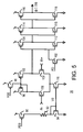
- FIG. 5 is a schematic of a differential-to-single-ended buffer.
- Buffer 30 Receives the Q+ and Q ⁇ outputs from a differential toggle flip-flop. Depending on which clock ⁇ 1 to ⁇ 16 is to be generated by the buffer 30 , the Q+ and Q ⁇ outputs from the flip-flop can be applied to either IN+, IN ⁇ , respectively, for non-inverting buffering, or to IN ⁇ , IN+, respectively, for inversion.
- a bias voltage VB is generated by a current flowing through p-channel bias transistor 90 , resistor 92 , and n-channel bias transistor 94 , which has its gate and drain connected together to generate VB.
- Bias voltage VB is applied to the gate of n-channel tail transistor 110 , which sinks a current from the differential sense amplifier.
- Differential inputs IN+, IN ⁇ are applied to the gates of n-channel differential transistors 108 , 106 , respectively.
- Current-mirror transistors 96 , 100 are p-channel transistors with their gates connected together and to the drain of transistors 96 , 106 .
- the single-ended output is taken from the drains of transistors 100 , 108 .
- Transistors 104 , 112 form the first inverter, transistors 114 , 116 the second inverter, and transistors 116 , 118 the final inverter that drives one of the 16 single-ended clocks ⁇ 1:16.
- the buffer can be powered down by driving PD high and PDB low. Then power-down n-channel transistor 102 drives the gates of first inverter transistors 104 , 112 low. This forces the output into a constant high state.
- the low PDB turns on power-down p-channel transistor 98 , which drives the gates of current-mirror transistors 96 , 100 high, turning off current-mirror transistors 96 , 100 .
- the low PDB signal to the gate of p-channel bias transistor 90 turns it off, turning off the bias generator and causing bias VB to fall to ground. Thus tail transistor 110 also shuts off.
- FIG. 6 is a schematic of the delay stages operating in a voltage-controlled oscillator (VCO).
- Delay stages 14 A- 14 D can operate under voltage-bias control as VCO 15 for a Phase-locked loop (PLL).
- a voltage input VBIAS is applied to the gate of p-channel bias transistor 164 , which modulates the current passing through resistor 162 and n-channel bias transistor 166 .
- VBIAS rises, current is reduced, causing the gate and drain of n-channel bias transistor 166 to fall in voltage. Since the gate and drain of n-channel bias transistor 166 is a bias voltage VB, VB falls when VBIAS rises.
- First delay stage 14 A received DEL 4 B on the gate of n-channel differential transistor 126 , and DEL 4 on the gate of n-channel differential transistor 128 . These signals are crossed-over and fed back from last delay stage 14 D. Resistors 122 , 124 produce voltages for complement output DEL 1 B and true output DEL 1 , respectively.
- Second delay stage 14 B receives DEL 1 on the gate of n-channel differential transistor 138 , which modulates current through resistor 134 to generate DEL 2 B. Second delay stage 14 B also receives DEL 1 B on the gate of n-channel differential transistor 136 , which modulates current through resistor 132 to generate DEL 2 . As DEL 1 rises and DEL 1 B falls, the current through differential transistor 138 rises, lowering the voltage of its drain, DEL 2 B. The current through differential transistor 136 falls, raising the voltage of its drain, DEL 2 . Thus delay stage 14 B is non-inverting from DEL 1 to DEL 2 , and from DEL 1 B to DEL 2 B, but inverting from DEL 1 to DEL 2 B and from DEL 1 B to DEL 2 .
- Third and fourth delays stages 14 C, 14 D operate in a similar manner.
- resistor 142 and transistor 146 invert DEL 2 to generate DEL 3 B, while resistor 144 and transistor 148 invert DEL 2 B to generate DEL 3 .
- resistor 152 and transistor 156 invert DEL 3 B to generate DEL 4
- resistor 154 and transistor 158 invert DEL 3 to generate DEL 4 B.
- the outputs DEL 1 - 4 and DEL 1 B-DEL 4 B can be used to drive the CK+ and CK ⁇ inputs to the differential toggle flip-flops.
- the delays to any pair of true and complementary outputs, such as to DEL 1 , DEL 1 B, are closely matched since differential signals and logic are used.
- the current-steering logic is very fast and sensitive to small changes in differential input voltages.
- Bias voltage VB is applied to the gates of tail transistors 130 , 140 , 150 , 160 , which control the tail currents and delays of delay stages 14 A- 14 D. As VBIAS rises, VB falls, tail current fall, and delays increase. Since the total loop delay determines the clock period, VBIAS can be used to adjust the clock period or frequency. The voltage input controls the period of oscillation, so the circuit operates as a VCO. Of course, separate voltage bias generators could be used for some or all delay stages to adjust relative delays.
- FIG. 7 shows the use of the differential delay stages as a VCO in a PLL.
- a reference clock is input to phase detector 202 and compared with a feedback clock.
- the feedback clock is one of the 16 clock phases ⁇ 1-16 from buffers 30 .
- a derivative of one or more of the clock phases ⁇ 1-16 can be fed back to phase detector 202 , such as by using a clock divider in the feedback path.
- Phase detector 202 compares the phase of the reference and feedback clocks, and generates up and down signals to charge pump 204 . Phase detector 202 can also compare phases and frequencies, rather than simply phases. The up and down signals cause charge pump 204 to charge or discharge a capacitance in filter 206 . This charging or discharging adjusts the control voltage VBIAS.
- the control voltage VBIAS is input to VCO 15 .
- VBIAS adjusts the tail currents in the delay stages 14 A- 14 D in VCO 15 .
- Changes in control voltage VBIAS adjust the delays in the delay stages, adjusting the output clock phases.
- the delay buffers are arranged in a twisted-ring arrangement, with the outputs of the last delay stage cross-coupled to the inputs of the first delay stage. This provides one inversion in the signal path through the delay stages, where each delay stage is encountered twice in the twisted loop.
- the true and complement outputs from delay stages 14 A- 14 D drive the differential clock inputs of differential toggle flip-flops 20 .
- the signals output by the delay stages are divided by two by the toggle flip-flops 20 .
- the differential outputs from differential toggle flip-flops 20 are converted to single-ended logic signals by buffers 30 to generate the sixteen clock phases ⁇ 1- ⁇ 16. Additional clock-selection logic (not shown) can be used to select one of the 16 clock phases for use as a system clock for an external system.
- the feedback is taken from one of the 16 clock phases, preferably the final clock phase ⁇ 16, although any clock phase can be used.
- Phase detector 202 and charge pump 204 adjust the VCO control voltage VBIAS to adjust the delays in the delay stages to match the reference clock.
- the reference clock and multi-phase output clocks ⁇ 1-16 operate at half the frequency of VCO 15 .
- FIG. 8 shows the use of the differential delay stages as an open-ended delay line in a delay-locked loop (DLL).
- DLL is similar to a PLL, but uses a delay line rather than an oscillator.
- the delay stages 14 A- 14 D are arranged in a single line without the feedback from last delay stage 14 D to first stage 14 A. Instead, the reference clock (or a derivative) is applied to the input of the first delay stage 14 A in delay line 14 ′. If the reference clock is not differential, a single-ended-to-differential converter (not shown) may be needed to generate true and complement versions of the reference clock to apply to the inputs of the first delay stage.
- the reference clock input to phase detector 202 is compared with a feedback clock.
- the feedback clock is one of the 16 clock phases ⁇ 1-16 from buffers 30 , or can be taken from the output of the last delay stage.
- a clock derivative can also be used.
- Phase detector 202 generates up and down signals to charge pump 204 , which charges or discharges a capacitance in filter 206 . This charging or discharging adjusts the control voltage VBIAS.
- the control voltage VBIAS is input to delay line 14 ′.
- VBIAS adjusts the tail currents in the delay stages 14 A- 14 D in delay line 14 ′.
- Changes in control voltage VBIAS adjust the delays in the delay stages, adjusting the output clock period.
- the true and complement outputs from delay stages 14 A- 14 D drive the differential clock inputs of differential toggle flip-flops 20 .
- the signals output by the delay stages are divided by two by the toggle flip-flops 20 .
- the differential outputs from differential toggle flip-flops 20 are converted to single-ended logic signals by buffers 30 to generate the sixteen clock phases ⁇ 1- ⁇ 16. Additional clock-selection logic (not shown) can be used to select one of the 16 clock phases for use as a system clock for an external system.
- the reference clock and multi-phase output clocks ⁇ 1-16 operate at half the frequency of delay line 14 ′ in this particular embodiment.
- FIG. 9 is an alternative embodiment of the twisted-ring oscillator using differential toggle flip-flops.
- Delay stages 14 A- 14 B are run at twice the frequency of the previous examples, or four times the reference clock frequency.
- the true and complement outputs DEL 1 - 4 , DEL 1 B-DEL 4 B are applied to the differential clock inputs CK+, CK ⁇ of first-level differential toggle flip-flops 40 , 42 , 44 , 46 .
- First-level differential toggle flip-flops 40 , 42 , 44 , 46 generate true and complement output signals at half the frequency of delay stages 14 A- 14 D. This additional dividing-down of the clocks allows for higher-speed delay stages to be used to generate a slower output clock than may be needed for some applications or processes.
- Each pair of true and complement outputs from first-level differential toggle flip-flops 40 , 42 , 44 , 46 drive a pair of differential toggle flip-flops 20 - 27 .
- the two differential toggle flip-flops 20 , 24 in a pair have opposite polarity of input connections so that one toggles on the rising edge and the other toggles on the falling edge of the divided-down clocks output by first-level differential toggle flip-flop 40 .
- Differential-to-single-ended buffers 30 convert the true and complement outputs from differential toggle flip-flops 20 - 27 to single-ended clock signals ⁇ 1-16.
- sixteen equally-spaced phases are generated with a frequency being one-quarter of the frequency of delay stages 14 A- 14 D.
- Negative or positive voltage feedback in the PLL or DLL loop can be used, depending on the polarity of voltage bias control of the delay-stage currents.
- Several bias voltage lines can be used to separately adjust tail currents and delays of a subset of the delay stages, or individual delay stages.
- the loading on the outputs of the delay stages 14 A- 14 D should be matched as closely as possible to match delays, as should the loading on the outputs of differential toggle flip-flops 20 - 27 .
- Differential signaling allows for slower, less expensive manufacturing processes to be used. Erratic and multiple oscillation are avoided by using few delay stages, while the differential toggle flip-flops allows for many taps or clock phases to be generated from the few delay stages.
- the number of stages can be varied. For example, each stage generates 4 clocks in the examples shown, so five stages would generate 20 clocks, 3 stages would generate 12 clocks, seven stages would generate 35 clocks with clocks being spaced by 1/n of the period, such as 1/20 for 5 stages, 1/12 for 3 stages, or 1/35 for 7 stages.
- the feedback to the phase comparator could use a programmable clock selector to effectively increase or decrease the number of stages in the control loop that sets the stage delays. Some embodiments could use no divide by two and still create twice the number of clock phases as VCO stages. Rather than use single-ended clocks, the clock generator could generate differential clocks. The final differential-to-single-ended converters could then be eliminated.
Abstract
Description
Claims (20)
Priority Applications (1)
| Application Number | Priority Date | Filing Date | Title |
|---|---|---|---|
| US09/683,040 US6426662B1 (en) | 2001-11-12 | 2001-11-12 | Twisted-ring oscillator and delay line generating multiple phases using differential dividers and comparators to match delays |
Applications Claiming Priority (1)
| Application Number | Priority Date | Filing Date | Title |
|---|---|---|---|
| US09/683,040 US6426662B1 (en) | 2001-11-12 | 2001-11-12 | Twisted-ring oscillator and delay line generating multiple phases using differential dividers and comparators to match delays |
Publications (1)
| Publication Number | Publication Date |
|---|---|
| US6426662B1 true US6426662B1 (en) | 2002-07-30 |
Family
ID=24742310
Family Applications (1)
| Application Number | Title | Priority Date | Filing Date |
|---|---|---|---|
| US09/683,040 Expired - Fee Related US6426662B1 (en) | 2001-11-12 | 2001-11-12 | Twisted-ring oscillator and delay line generating multiple phases using differential dividers and comparators to match delays |
Country Status (1)
| Country | Link |
|---|---|
| US (1) | US6426662B1 (en) |
Cited By (54)
| Publication number | Priority date | Publication date | Assignee | Title |
|---|---|---|---|---|
| US20040036500A1 (en) * | 2002-08-08 | 2004-02-26 | Bratt Adrian Harvey | Semiconductor devices |
| US6727764B2 (en) * | 2002-03-08 | 2004-04-27 | Sirific Wireless Corporation | Generation of virtual local oscillator inputs for use in direct conversion radio systems |
| US20040090828A1 (en) * | 2000-07-27 | 2004-05-13 | Junichi Okamura | Semiconductor integrated circuit |
| US20040108872A1 (en) * | 2002-12-09 | 2004-06-10 | Shen-Iuan Liu | Voltage-controlled delay line with reduced timing errors and jitters |
| US6750799B1 (en) * | 1999-11-03 | 2004-06-15 | Ion E. Opris | A/D conversion technique using digital averages |
| US20040160256A1 (en) * | 2003-02-18 | 2004-08-19 | Matsushita Electric Industrial Co., Ltd. | Semiconductor device |
| EP1463201A1 (en) * | 2003-03-25 | 2004-09-29 | Infineon Technologies AG | Frequency divider controlled by current signal injection |
| US6809566B1 (en) * | 2003-07-30 | 2004-10-26 | National Semiconductor Corporation | Low power differential-to-single-ended converter with good duty cycle performance |
| US20050190474A1 (en) * | 2004-02-26 | 2005-09-01 | Hitachi Global Technologies Netherlands B.V. | Method and apparatus for providing write pre-compensation using a read timing path |
| US20050237122A1 (en) * | 2004-04-21 | 2005-10-27 | Texas Instruments Incorporated | Cross coupled voltage controlled oscillator |
| US20060011097A1 (en) * | 2004-04-08 | 2006-01-19 | Canon Kabushiki Kaisha | Ink jet recording ink, ink jet recording method, ink cartridge, and ink jet recording apparatus |
| US7002764B2 (en) | 2004-02-26 | 2006-02-21 | Hitachi Global Storage Technologies Netherlands B.V. | Method and apparatus for providing generalized write pre-compensation |
| US20060087908A1 (en) * | 2004-07-19 | 2006-04-27 | Micron Technology, Inc. | Delay stage-interweaved analog DLL/PLL |
| US20060238240A1 (en) * | 2002-06-25 | 2006-10-26 | Bogdan John W | Digital signal processing of multi-sampled phase |
| US7135899B1 (en) * | 2003-06-27 | 2006-11-14 | Cypress Semiconductor Corp. | System and method for reducing skew in complementary signals that can be used to synchronously clock a double data rate output |
| JP2007006492A (en) * | 2005-06-21 | 2007-01-11 | Samsung Electronics Co Ltd | Phase locked loop circuit and method of locking phase |
| US20070069779A1 (en) * | 2005-09-29 | 2007-03-29 | Hynix Semiconductor Inc. | Delay locked loop circuit |
| US20070126483A1 (en) * | 2005-12-02 | 2007-06-07 | Wei-Ming Chen | Gate driver |
| US20080231376A1 (en) * | 2007-03-14 | 2008-09-25 | Sanyo Electric Co., Ltd. | Oscillation circuit controlling phase difference of output signals |
| US20090045850A1 (en) * | 2007-04-09 | 2009-02-19 | Multigig, Inc. | Rtwo-based down converter |
| US20090115467A1 (en) * | 2007-11-05 | 2009-05-07 | Hynix Semiconductor Inc. | Semiconductor device and operation method thereof |
| US20100086075A1 (en) * | 2008-07-29 | 2010-04-08 | Fujitsu Limited | Parallel Generation and Matching of a Deskew Channel |
| US20100091927A1 (en) * | 2008-07-29 | 2010-04-15 | Fujitsu Limited | Clock and Data Recovery (CDR) Using Phase Interpolation |
| US20100104057A1 (en) * | 2008-07-29 | 2010-04-29 | Fujitsu Limited | Clock and Data Recovery with a Data Aligner |
| US20100103762A1 (en) * | 2008-10-23 | 2010-04-29 | Joseph Tzou | Memory device and method |
| US20100241918A1 (en) * | 2009-03-20 | 2010-09-23 | Fujitsu Limited | Clock and data recovery for differential quadrature phase shift keying |
| US20100271076A1 (en) * | 2009-04-27 | 2010-10-28 | Sun Microsystems, Inc. | Precision sampling circuit |
| US20100271100A1 (en) * | 2009-04-27 | 2010-10-28 | Sun Microsystems, Inc. | Minimal bubble voltage regulator |
| US20100271099A1 (en) * | 2009-04-27 | 2010-10-28 | Sun Microsystems, Inc. | Fine grain timing |
| US20110012685A1 (en) * | 2009-01-09 | 2011-01-20 | Hamid Partovi | Wide-band Low-voltage IQ-generating Ring-oscillator-based CMOS VCO |
| US8242823B2 (en) | 2009-04-27 | 2012-08-14 | Oracle America, Inc. | Delay chain initialization |
| US8300753B2 (en) | 2008-07-29 | 2012-10-30 | Fujitsu Limited | Triple loop clock and data recovery (CDR) |
| US20120274359A1 (en) * | 2010-03-11 | 2012-11-01 | Altera Corporation | High-speed differential comparator circuitry with accurately adjustable threshold |
| US8355478B1 (en) | 2009-05-29 | 2013-01-15 | Honeywell International Inc. | Circuit for aligning clock to parallel data |
| US8410858B2 (en) | 1999-01-22 | 2013-04-02 | Analog Devices, Inc. | Electronic circuitry |
| US8487710B2 (en) | 2011-12-12 | 2013-07-16 | Analog Devices, Inc. | RTWO-based pulse width modulator |
| US8581668B2 (en) | 2011-12-20 | 2013-11-12 | Analog Devices, Inc. | Oscillator regeneration device |
| US8633774B2 (en) | 2000-05-11 | 2014-01-21 | Analog Devices, Inc. | Electronic pulse generator and oscillator |
| US8669818B2 (en) | 2007-03-29 | 2014-03-11 | Analog Devices, Inc. | Wave reversing system and method for a rotary traveling wave oscillator |
| US8742857B2 (en) | 2008-05-15 | 2014-06-03 | Analog Devices, Inc. | Inductance enhanced rotary traveling wave oscillator circuit and method |
| KR101405702B1 (en) | 2008-05-28 | 2014-06-10 | 마이크론 테크놀로지, 인크. | Apparatus and method for multi-phase clock generation |
| US20140266371A1 (en) * | 2013-03-15 | 2014-09-18 | Samsung Electronics Co., Ltd. | Multi-phase generator |
| US20150194968A1 (en) * | 2014-01-03 | 2015-07-09 | Oracle International Corporation | Phase Aligner with Short Lock Time |
| US20160028379A1 (en) * | 2014-07-28 | 2016-01-28 | Megachips Corporation | Clock generator |
| US20180019657A1 (en) * | 2016-07-14 | 2018-01-18 | Fuji Electric Co., Ltd. | Control circuit for switching power supply apparatus |
| CN109428568A (en) * | 2017-08-31 | 2019-03-05 | 爱思开海力士有限公司 | The method of semiconductor devices and arrangement ring oscillator with ring oscillator |
| US10277233B2 (en) | 2016-10-07 | 2019-04-30 | Analog Devices, Inc. | Apparatus and methods for frequency tuning of rotary traveling wave oscillators |
| US10312922B2 (en) | 2016-10-07 | 2019-06-04 | Analog Devices, Inc. | Apparatus and methods for rotary traveling wave oscillators |
| US10756710B2 (en) | 2017-04-11 | 2020-08-25 | Chaologix, Inc. | Integrated ring oscillator clock generator |
| CN112073059A (en) * | 2020-08-27 | 2020-12-11 | 灿芯半导体(上海)有限公司 | DLL circuit |
| US11086353B2 (en) * | 2018-03-20 | 2021-08-10 | Shenzhen GOODIX Technology Co., Ltd. | Fractional clock generator with low power and low noise |
| US11264949B2 (en) | 2020-06-10 | 2022-03-01 | Analog Devices International Unlimited Company | Apparatus and methods for rotary traveling wave oscillators |
| US11527992B2 (en) | 2019-09-19 | 2022-12-13 | Analog Devices International Unlimited Company | Rotary traveling wave oscillators with distributed stubs |
| US11539353B2 (en) | 2021-02-02 | 2022-12-27 | Analog Devices International Unlimited Company | RTWO-based frequency multiplier |
Citations (17)
| Publication number | Priority date | Publication date | Assignee | Title |
|---|---|---|---|---|
| US3671872A (en) | 1971-03-26 | 1972-06-20 | Telemation | High frequency multiple phase signal generator |
| US4805795A (en) | 1986-12-27 | 1989-02-21 | Toyo Seikan Kaisha Ltd. | Butt-welded cans and process for manufacturing the same |
| US5051970A (en) | 1987-05-08 | 1991-09-24 | Nippon Telegraph And Telephone Corporation | Magneto-optic recording system with overwrite capability |
| US5077529A (en) | 1989-07-19 | 1991-12-31 | Level One Communications, Inc. | Wide bandwidth digital phase locked loop with reduced low frequency intrinsic jitter |
| US5109394A (en) | 1990-12-24 | 1992-04-28 | Ncr Corporation | All digital phase locked loop |
| US5120990A (en) | 1990-06-29 | 1992-06-09 | Analog Devices, Inc. | Apparatus for generating multiple phase clock signals and phase detector therefor |
| US5422835A (en) | 1993-07-28 | 1995-06-06 | International Business Machines Corporation | Digital clock signal multiplier circuit |
| US5495205A (en) | 1995-01-06 | 1996-02-27 | Robert D. Atkins | Digital controlled oscillator and method thereof |
| US5532633A (en) | 1993-12-03 | 1996-07-02 | Nec Corporaton | Clock generating circuit generating a plurality of non-overlapping clock signals |
| US5544203A (en) | 1993-02-17 | 1996-08-06 | Texas Instruments Incorporated | Fine resolution digital delay line with coarse and fine adjustment stages |
| US5673295A (en) * | 1995-04-13 | 1997-09-30 | Synopsis, Incorporated | Method and apparatus for generating and synchronizing a plurality of digital signals |
| US5970110A (en) | 1998-01-09 | 1999-10-19 | Neomagic Corp. | Precise, low-jitter fractional divider using counter of rotating clock phases |
| US6037818A (en) | 1997-03-19 | 2000-03-14 | Advantest Corp. | High resolution delay circuit having coarse and fine delay circuits |
| US6094076A (en) | 1997-06-13 | 2000-07-25 | Nec Corporation | Method and apparatus for controlling clock signals |
| US6101197A (en) | 1997-09-18 | 2000-08-08 | Micron Technology, Inc. | Method and apparatus for adjusting the timing of signals over fine and coarse ranges |
| US6100735A (en) | 1998-11-19 | 2000-08-08 | Centillium Communications, Inc. | Segmented dual delay-locked loop for precise variable-phase clock generation |
| US6163226A (en) * | 1998-06-01 | 2000-12-19 | Lucent Technologies, Inc. | Current-controlled p-channel transistor-based ring oscillator |
-
2001
- 2001-11-12 US US09/683,040 patent/US6426662B1/en not_active Expired - Fee Related
Patent Citations (17)
| Publication number | Priority date | Publication date | Assignee | Title |
|---|---|---|---|---|
| US3671872A (en) | 1971-03-26 | 1972-06-20 | Telemation | High frequency multiple phase signal generator |
| US4805795A (en) | 1986-12-27 | 1989-02-21 | Toyo Seikan Kaisha Ltd. | Butt-welded cans and process for manufacturing the same |
| US5051970A (en) | 1987-05-08 | 1991-09-24 | Nippon Telegraph And Telephone Corporation | Magneto-optic recording system with overwrite capability |
| US5077529A (en) | 1989-07-19 | 1991-12-31 | Level One Communications, Inc. | Wide bandwidth digital phase locked loop with reduced low frequency intrinsic jitter |
| US5120990A (en) | 1990-06-29 | 1992-06-09 | Analog Devices, Inc. | Apparatus for generating multiple phase clock signals and phase detector therefor |
| US5109394A (en) | 1990-12-24 | 1992-04-28 | Ncr Corporation | All digital phase locked loop |
| US5544203A (en) | 1993-02-17 | 1996-08-06 | Texas Instruments Incorporated | Fine resolution digital delay line with coarse and fine adjustment stages |
| US5422835A (en) | 1993-07-28 | 1995-06-06 | International Business Machines Corporation | Digital clock signal multiplier circuit |
| US5532633A (en) | 1993-12-03 | 1996-07-02 | Nec Corporaton | Clock generating circuit generating a plurality of non-overlapping clock signals |
| US5495205A (en) | 1995-01-06 | 1996-02-27 | Robert D. Atkins | Digital controlled oscillator and method thereof |
| US5673295A (en) * | 1995-04-13 | 1997-09-30 | Synopsis, Incorporated | Method and apparatus for generating and synchronizing a plurality of digital signals |
| US6037818A (en) | 1997-03-19 | 2000-03-14 | Advantest Corp. | High resolution delay circuit having coarse and fine delay circuits |
| US6094076A (en) | 1997-06-13 | 2000-07-25 | Nec Corporation | Method and apparatus for controlling clock signals |
| US6101197A (en) | 1997-09-18 | 2000-08-08 | Micron Technology, Inc. | Method and apparatus for adjusting the timing of signals over fine and coarse ranges |
| US5970110A (en) | 1998-01-09 | 1999-10-19 | Neomagic Corp. | Precise, low-jitter fractional divider using counter of rotating clock phases |
| US6163226A (en) * | 1998-06-01 | 2000-12-19 | Lucent Technologies, Inc. | Current-controlled p-channel transistor-based ring oscillator |
| US6100735A (en) | 1998-11-19 | 2000-08-08 | Centillium Communications, Inc. | Segmented dual delay-locked loop for precise variable-phase clock generation |
Cited By (89)
| Publication number | Priority date | Publication date | Assignee | Title |
|---|---|---|---|---|
| US8947168B2 (en) | 1999-01-22 | 2015-02-03 | Analog Devices, Inc. | Electronic circuitry |
| US8410858B2 (en) | 1999-01-22 | 2013-04-02 | Analog Devices, Inc. | Electronic circuitry |
| US6750799B1 (en) * | 1999-11-03 | 2004-06-15 | Ion E. Opris | A/D conversion technique using digital averages |
| US8633774B2 (en) | 2000-05-11 | 2014-01-21 | Analog Devices, Inc. | Electronic pulse generator and oscillator |
| US20040090828A1 (en) * | 2000-07-27 | 2004-05-13 | Junichi Okamura | Semiconductor integrated circuit |
| US6727764B2 (en) * | 2002-03-08 | 2004-04-27 | Sirific Wireless Corporation | Generation of virtual local oscillator inputs for use in direct conversion radio systems |
| US7564934B2 (en) * | 2002-06-25 | 2009-07-21 | John W. Bogdan | Digital signal processing of multi-sampled phase |
| US20060238240A1 (en) * | 2002-06-25 | 2006-10-26 | Bogdan John W | Digital signal processing of multi-sampled phase |
| US20040036500A1 (en) * | 2002-08-08 | 2004-02-26 | Bratt Adrian Harvey | Semiconductor devices |
| US20040108872A1 (en) * | 2002-12-09 | 2004-06-10 | Shen-Iuan Liu | Voltage-controlled delay line with reduced timing errors and jitters |
| US6756818B1 (en) * | 2002-12-09 | 2004-06-29 | Mediatek Incorporation | Voltage-controlled delay line with reduced timing errors and jitters |
| US7183829B2 (en) * | 2003-02-18 | 2007-02-27 | Matsushita Electric Industrial Co., Ltd. | Semiconductor device including a plurality of circuit blocks provided on a chip and having different functions |
| US20040160256A1 (en) * | 2003-02-18 | 2004-08-19 | Matsushita Electric Industrial Co., Ltd. | Semiconductor device |
| EP1463201A1 (en) * | 2003-03-25 | 2004-09-29 | Infineon Technologies AG | Frequency divider controlled by current signal injection |
| US7135899B1 (en) * | 2003-06-27 | 2006-11-14 | Cypress Semiconductor Corp. | System and method for reducing skew in complementary signals that can be used to synchronously clock a double data rate output |
| US7061277B1 (en) | 2003-07-30 | 2006-06-13 | National Semiconductor Corporation | Low power differential-to-single-ended converter with good duty cycle performance |
| US6809566B1 (en) * | 2003-07-30 | 2004-10-26 | National Semiconductor Corporation | Low power differential-to-single-ended converter with good duty cycle performance |
| US7002764B2 (en) | 2004-02-26 | 2006-02-21 | Hitachi Global Storage Technologies Netherlands B.V. | Method and apparatus for providing generalized write pre-compensation |
| US7123430B2 (en) | 2004-02-26 | 2006-10-17 | Hitachi Global Storage Technologies Netherlands B.V. | Method and apparatus for providing write pre-compensation using a read timing path |
| US7123429B2 (en) | 2004-02-26 | 2006-10-17 | Hitachi Global Storage Technologies Netherlands B.V. | Method and apparatus for providing write pre-compensation using a read timing path |
| US20050200996A1 (en) * | 2004-02-26 | 2005-09-15 | Hitachi Global Storage Technologies Netherlands B.V. | Method and apparatus for providing write pre-compensation using a read timing path |
| US20050190474A1 (en) * | 2004-02-26 | 2005-09-01 | Hitachi Global Technologies Netherlands B.V. | Method and apparatus for providing write pre-compensation using a read timing path |
| US20060011097A1 (en) * | 2004-04-08 | 2006-01-19 | Canon Kabushiki Kaisha | Ink jet recording ink, ink jet recording method, ink cartridge, and ink jet recording apparatus |
| US7071789B2 (en) * | 2004-04-21 | 2006-07-04 | Texas Instruments Incorporated | Cross coupled voltage controlled oscillator |
| US20050237122A1 (en) * | 2004-04-21 | 2005-10-27 | Texas Instruments Incorporated | Cross coupled voltage controlled oscillator |
| US7382678B2 (en) * | 2004-07-19 | 2008-06-03 | Micron Technology, Inc. | Delay stage-interweaved analog DLL/PLL |
| US20060087908A1 (en) * | 2004-07-19 | 2006-04-27 | Micron Technology, Inc. | Delay stage-interweaved analog DLL/PLL |
| US7835205B2 (en) | 2004-07-19 | 2010-11-16 | Micron Technology, Inc. | Delay stage-interweaved analog DLL/PLL |
| JP2007006492A (en) * | 2005-06-21 | 2007-01-11 | Samsung Electronics Co Ltd | Phase locked loop circuit and method of locking phase |
| US7449927B2 (en) | 2005-09-29 | 2008-11-11 | Hynix Semiconductor Inc. | Delay locked loop circuit |
| US20070069779A1 (en) * | 2005-09-29 | 2007-03-29 | Hynix Semiconductor Inc. | Delay locked loop circuit |
| US7741891B2 (en) | 2005-09-29 | 2010-06-22 | Hynix Semiconductor, Inc. | Delay locked loop circuit |
| US20070126483A1 (en) * | 2005-12-02 | 2007-06-07 | Wei-Ming Chen | Gate driver |
| US20080231376A1 (en) * | 2007-03-14 | 2008-09-25 | Sanyo Electric Co., Ltd. | Oscillation circuit controlling phase difference of output signals |
| US8669818B2 (en) | 2007-03-29 | 2014-03-11 | Analog Devices, Inc. | Wave reversing system and method for a rotary traveling wave oscillator |
| US8913978B2 (en) | 2007-04-09 | 2014-12-16 | Analog Devices, Inc. | RTWO-based down converter |
| US20090045850A1 (en) * | 2007-04-09 | 2009-02-19 | Multigig, Inc. | Rtwo-based down converter |
| US8283962B2 (en) * | 2007-11-05 | 2012-10-09 | Hynix Semiconductor Inc. | Semiconductor device and operation method thereof for generating phase clock signals |
| US20090115467A1 (en) * | 2007-11-05 | 2009-05-07 | Hynix Semiconductor Inc. | Semiconductor device and operation method thereof |
| US8742857B2 (en) | 2008-05-15 | 2014-06-03 | Analog Devices, Inc. | Inductance enhanced rotary traveling wave oscillator circuit and method |
| KR101405702B1 (en) | 2008-05-28 | 2014-06-10 | 마이크론 테크놀로지, 인크. | Apparatus and method for multi-phase clock generation |
| US8300754B2 (en) | 2008-07-29 | 2012-10-30 | Fujitsu Limited | Clock and data recovery with a data aligner |
| US20100104057A1 (en) * | 2008-07-29 | 2010-04-29 | Fujitsu Limited | Clock and Data Recovery with a Data Aligner |
| US8411782B2 (en) | 2008-07-29 | 2013-04-02 | Fujitsu Limited | Parallel generation and matching of a deskew channel |
| US8718217B2 (en) * | 2008-07-29 | 2014-05-06 | Fujitsu Limited | Clock and data recovery (CDR) using phase interpolation |
| US20100086075A1 (en) * | 2008-07-29 | 2010-04-08 | Fujitsu Limited | Parallel Generation and Matching of a Deskew Channel |
| US20100091927A1 (en) * | 2008-07-29 | 2010-04-15 | Fujitsu Limited | Clock and Data Recovery (CDR) Using Phase Interpolation |
| US8300753B2 (en) | 2008-07-29 | 2012-10-30 | Fujitsu Limited | Triple loop clock and data recovery (CDR) |
| US8149643B2 (en) | 2008-10-23 | 2012-04-03 | Cypress Semiconductor Corporation | Memory device and method |
| US20100103762A1 (en) * | 2008-10-23 | 2010-04-29 | Joseph Tzou | Memory device and method |
| US8358557B2 (en) | 2008-10-23 | 2013-01-22 | Cypress Semiconductor Corporation | Memory device and method |
| US20110012685A1 (en) * | 2009-01-09 | 2011-01-20 | Hamid Partovi | Wide-band Low-voltage IQ-generating Ring-oscillator-based CMOS VCO |
| US20100241918A1 (en) * | 2009-03-20 | 2010-09-23 | Fujitsu Limited | Clock and data recovery for differential quadrature phase shift keying |
| US8320770B2 (en) | 2009-03-20 | 2012-11-27 | Fujitsu Limited | Clock and data recovery for differential quadrature phase shift keying |
| US20100271076A1 (en) * | 2009-04-27 | 2010-10-28 | Sun Microsystems, Inc. | Precision sampling circuit |
| US20100271099A1 (en) * | 2009-04-27 | 2010-10-28 | Sun Microsystems, Inc. | Fine grain timing |
| US8198931B2 (en) | 2009-04-27 | 2012-06-12 | Oracle America, Inc. | Fine grain timing |
| US8179165B2 (en) * | 2009-04-27 | 2012-05-15 | Oracle America, Inc. | Precision sampling circuit |
| US8283960B2 (en) | 2009-04-27 | 2012-10-09 | Oracle America, Inc. | Minimal bubble voltage regulator |
| US20100271100A1 (en) * | 2009-04-27 | 2010-10-28 | Sun Microsystems, Inc. | Minimal bubble voltage regulator |
| US8242823B2 (en) | 2009-04-27 | 2012-08-14 | Oracle America, Inc. | Delay chain initialization |
| US8355478B1 (en) | 2009-05-29 | 2013-01-15 | Honeywell International Inc. | Circuit for aligning clock to parallel data |
| US8610466B2 (en) * | 2010-03-11 | 2013-12-17 | Altera Corporation | High-speed differential comparator circuitry with accurately adjustable threshold |
| US20120274359A1 (en) * | 2010-03-11 | 2012-11-01 | Altera Corporation | High-speed differential comparator circuitry with accurately adjustable threshold |
| US8487710B2 (en) | 2011-12-12 | 2013-07-16 | Analog Devices, Inc. | RTWO-based pulse width modulator |
| US8581668B2 (en) | 2011-12-20 | 2013-11-12 | Analog Devices, Inc. | Oscillator regeneration device |
| CN104052468B (en) * | 2013-03-15 | 2018-07-24 | 三星电子株式会社 | Leggy generator |
| US20140266371A1 (en) * | 2013-03-15 | 2014-09-18 | Samsung Electronics Co., Ltd. | Multi-phase generator |
| US8981828B2 (en) * | 2013-03-15 | 2015-03-17 | Samsung Electronics Co., Ltd. | Multi-phase generator |
| US20150194968A1 (en) * | 2014-01-03 | 2015-07-09 | Oracle International Corporation | Phase Aligner with Short Lock Time |
| US9136850B2 (en) * | 2014-01-03 | 2015-09-15 | Oracle International Corporation | Phase aligner with short lock time |
| US20160028379A1 (en) * | 2014-07-28 | 2016-01-28 | Megachips Corporation | Clock generator |
| CN105306050A (en) * | 2014-07-28 | 2016-02-03 | 株式会社巨晶片 | Clock generator |
| JP2016031581A (en) * | 2014-07-28 | 2016-03-07 | 株式会社メガチップス | Clock generation circuit |
| US9647642B2 (en) * | 2014-07-28 | 2017-05-09 | Megachips Corporation | Clock phase adjustment mechanism of a ring oscillator using a phase control signal |
| CN105306050B (en) * | 2014-07-28 | 2020-04-24 | 株式会社巨晶片 | Clock generation circuit |
| US10277106B2 (en) * | 2016-07-14 | 2019-04-30 | Fuji Electric Co., Ltd. | Control circuit for switching power supply apparatus |
| US20180019657A1 (en) * | 2016-07-14 | 2018-01-18 | Fuji Electric Co., Ltd. | Control circuit for switching power supply apparatus |
| US10277233B2 (en) | 2016-10-07 | 2019-04-30 | Analog Devices, Inc. | Apparatus and methods for frequency tuning of rotary traveling wave oscillators |
| US10312922B2 (en) | 2016-10-07 | 2019-06-04 | Analog Devices, Inc. | Apparatus and methods for rotary traveling wave oscillators |
| US10756741B2 (en) | 2016-10-07 | 2020-08-25 | Analog Devices, Inc. | Apparatus and methods for rotary traveling wave oscillators |
| US10756710B2 (en) | 2017-04-11 | 2020-08-25 | Chaologix, Inc. | Integrated ring oscillator clock generator |
| CN109428568A (en) * | 2017-08-31 | 2019-03-05 | 爱思开海力士有限公司 | The method of semiconductor devices and arrangement ring oscillator with ring oscillator |
| US11086353B2 (en) * | 2018-03-20 | 2021-08-10 | Shenzhen GOODIX Technology Co., Ltd. | Fractional clock generator with low power and low noise |
| US11527992B2 (en) | 2019-09-19 | 2022-12-13 | Analog Devices International Unlimited Company | Rotary traveling wave oscillators with distributed stubs |
| US11264949B2 (en) | 2020-06-10 | 2022-03-01 | Analog Devices International Unlimited Company | Apparatus and methods for rotary traveling wave oscillators |
| CN112073059A (en) * | 2020-08-27 | 2020-12-11 | 灿芯半导体(上海)有限公司 | DLL circuit |
| CN112073059B (en) * | 2020-08-27 | 2023-11-21 | 灿芯半导体(上海)股份有限公司 | DLL circuit |
| US11539353B2 (en) | 2021-02-02 | 2022-12-27 | Analog Devices International Unlimited Company | RTWO-based frequency multiplier |
Similar Documents
| Publication | Publication Date | Title |
|---|---|---|
| US6426662B1 (en) | Twisted-ring oscillator and delay line generating multiple phases using differential dividers and comparators to match delays | |
| JP3390054B2 (en) | Polyphase output oscillator | |
| US20060001496A1 (en) | Array oscillator and polyphase clock generator | |
| US5815042A (en) | Duty cycled control implemented within a frequency synthesizer | |
| US7911282B2 (en) | Voltage-controlled oscillator including plurality of delay cells | |
| JPH10261943A (en) | Delay circuit and oscillation circuit using the same | |
| US8237480B2 (en) | Clock generation circuit and integrated circuit | |
| JP4129010B2 (en) | Delay circuit | |
| JP2008135835A (en) | Pll circuit | |
| JP6612500B2 (en) | Clock generation circuit | |
| US7388442B2 (en) | Digitally controlled oscillator for reduced power over process variations | |
| US6603339B2 (en) | Precision aligned multiple concurrent duty cycles from a programmable duty cycle generator | |
| US20190149141A1 (en) | Clock doublers with duty cycle correction | |
| JP2009153084A (en) | Variable delay circuit and control method thereof | |
| US6259295B1 (en) | Variable phase shifting clock generator | |
| US6509771B1 (en) | Enhanced operational frequency for a precise and programmable duty cycle generator | |
| JP4992947B2 (en) | Parallel-serial converter and parallel data output device | |
| US6577202B1 (en) | Multiple duty cycle tap points for a precise and programmable duty cycle generator | |
| US20030090330A1 (en) | Voltage controlled oscillation circuit having easily controllable oscillation characteristic and capable of generating high frequency and low frequency internal clocks | |
| US7477111B2 (en) | Digitally controlled oscillator | |
| JP2008312212A (en) | Wide range interpolative voltage controlled oscillator | |
| JP2004282360A (en) | Phase control circuit | |
| US9537476B1 (en) | Level shifter with low duty cycle variation | |
| US7098710B1 (en) | Multi-speed delay-locked loop | |
| JPH09326692A (en) | Phase locked loop circuit |
Legal Events
| Date | Code | Title | Description |
|---|---|---|---|
| AS | Assignment |
Owner name: PERICOM SEMICONDUCTOR CORP., CALIFORNIA Free format text: ASSIGNMENT OF ASSIGNORS INTEREST;ASSIGNOR:ARCUS, CHRISTOPHER G.;REEL/FRAME:012442/0045 Effective date: 20020209 |
|
| FEPP | Fee payment procedure |
Free format text: PAT HOLDER NO LONGER CLAIMS SMALL ENTITY STATUS, ENTITY STATUS SET TO UNDISCOUNTED (ORIGINAL EVENT CODE: STOL); ENTITY STATUS OF PATENT OWNER: LARGE ENTITY |
|
| FPAY | Fee payment |
Year of fee payment: 4 |
|
| FPAY | Fee payment |
Year of fee payment: 8 |
|
| REMI | Maintenance fee reminder mailed | ||
| LAPS | Lapse for failure to pay maintenance fees | ||
| STCH | Information on status: patent discontinuation |
Free format text: PATENT EXPIRED DUE TO NONPAYMENT OF MAINTENANCE FEES UNDER 37 CFR 1.362 |
|
| FP | Lapsed due to failure to pay maintenance fee |
Effective date: 20140730 |
|
| AS | Assignment |
Owner name: DIODES INCORPORATED, TEXAS Free format text: ASSIGNMENT OF ASSIGNORS INTEREST;ASSIGNOR:PERICOM SEMICONDUCTOR CORPORATION;REEL/FRAME:044975/0554 Effective date: 20171222 |