US6426237B2 - Method for producing optically planar surfaces for micro-electromechanical system devices - Google Patents
Method for producing optically planar surfaces for micro-electromechanical system devices Download PDFInfo
- Publication number
- US6426237B2 US6426237B2 US09/867,928 US86792801A US6426237B2 US 6426237 B2 US6426237 B2 US 6426237B2 US 86792801 A US86792801 A US 86792801A US 6426237 B2 US6426237 B2 US 6426237B2
- Authority
- US
- United States
- Prior art keywords
- layer
- channel
- overlap
- sacrificial
- optically planar
- Prior art date
- Legal status (The legal status is an assumption and is not a legal conclusion. Google has not performed a legal analysis and makes no representation as to the accuracy of the status listed.)
- Expired - Lifetime
Links
Images


Classifications
-
- B—PERFORMING OPERATIONS; TRANSPORTING
- B81—MICROSTRUCTURAL TECHNOLOGY
- B81C—PROCESSES OR APPARATUS SPECIALLY ADAPTED FOR THE MANUFACTURE OR TREATMENT OF MICROSTRUCTURAL DEVICES OR SYSTEMS
- B81C1/00—Manufacture or treatment of devices or systems in or on a substrate
- B81C1/00436—Shaping materials, i.e. techniques for structuring the substrate or the layers on the substrate
- B81C1/00555—Achieving a desired geometry, i.e. controlling etch rates, anisotropy or selectivity
- B81C1/00611—Processes for the planarisation of structures
-
- B—PERFORMING OPERATIONS; TRANSPORTING
- B81—MICROSTRUCTURAL TECHNOLOGY
- B81C—PROCESSES OR APPARATUS SPECIALLY ADAPTED FOR THE MANUFACTURE OR TREATMENT OF MICROSTRUCTURAL DEVICES OR SYSTEMS
- B81C2201/00—Manufacture or treatment of microstructural devices or systems
- B81C2201/01—Manufacture or treatment of microstructural devices or systems in or on a substrate
- B81C2201/0101—Shaping material; Structuring the bulk substrate or layers on the substrate; Film patterning
- B81C2201/0118—Processes for the planarization of structures
- B81C2201/0121—Processes for the planarization of structures involving addition of material followed by removal of parts of said material, i.e. subtractive planarization
Definitions
- This invention relates to micro-electromechanical devices, and more particularly to the optical planarity of micro-electromechanical device gratings.
- Micro-electromechanical spatial light modulators with a variety of designs have been used in applications such as display optical processing, printing, optical data storage and spectroscopy. These modulators produce spatial variations in the phase and/or amplitude of an incident light beam using arrays of individually addressable devices.
- CMP Chemical mechanical planarization
- the same technique can be used on a fill layer to obtain flat surfaces.
- many of the micromachined structures typically fall into the regime of wide (>10 ⁇ m wide) recesses and sparsely populated structures.
- One of the difficulties encountered with CMP planarization is the “dishing” effect which occurs in the planarization of wide recesses.
- the “dishing” effect during planarization results in thinning of a fill layer in wide recesses and a non-planar surface.
- the polish rate is affected by the topology of the surrounding areas with dishing becoming worse in sparsely populated regions. Therefore, dishing problems present a severe manufacturing constraint in micromachining.
- Non-uniform removal of a fill material across the wafer is also an important consideration in micromachining.
- a fill layer is a sacrificial layer, it must be removed outside of the active regions in order to assure adhesion of the release layers. Any residual sacrificial material outside of the active region will be attacked during release. Conventional polishing that ensures complete removal of a sacrificial layer outside of the active region will cause over-polishing and excess removal of the sacrificial material in the active regions.
- the dishing phenomenon is illustrated by reference to the schematic cross-sectional diagrams of FIG. 1 a and FIG. 1 b .
- Shown in FIG. 1 a is a substrate 100 onto which a first layer 150 is deposited.
- a narrow recess 110 and the wide recess 120 are shown formed in the first layer 150 .
- the surface of the first layer 150 will contain small areas 130 between recesses and large areas 140 between recesses 110 and 120 .
- Deposited over the first layer 150 and into both the narrow recess 110 and the wide recess 120 is a blanket conformal fill layer 160 .
- Shown in FIG. 1 b are the results of planarizing through a conventional chemical mechanical planarization(CMP) method and the blanket conformal fill layer 160 as illustrated in FIG. 1 a .
- CMP chemical mechanical planarization
- planarized filled wide recess 170 is severely dished in comparison with the surface of planarized filled narrow recess 180 .
- This marked contrast most resembles the large differences in the problems addressed by the semi-conductor industry versus those skilled in micro-electromechanical systems.
- Planarized filled narrow recess 180 has the narrow dishing experience in the semi-conductor industry, while planarized wide recess 170 has the complications experienced by the MEMS skilled artisans.
- a self-aligned mask formed by CMP and used within the severely dished planarized wide recess 170 would be completely polished away in any attempt to address the dishing phenomenon.
- FIG. 1 b There is also shown in FIG. 1 b the presence of a fill residue layer 190 , formed simultaneously over the small areas 130 and large areas 140 on the surface of the first layer 150 when the blanket conformal fill layer 160 is planarized through the chemical mechanical planarization (CMP) method to form the planarized filled recesses 180 and 170 .
- CMP chemical mechanical planarization
- the blanket conformal fill layer 160 when planarizing large areas of the blanket conformal fill layer 160 , generally of dimensions greater than about 1000 microns, the blanket conformal fill layer 160 will in addition to planarizing more rapidly over the wide recess 120 and forming a dish within the planarized filled wide recess 170 , simultaneously also polish more slowly over the large area 140 on the surface of the first layer 150 and leave the fill residue layer 190 formed over the large area 140 on the first layer 150 . Attempts to remove the fill residue layer 190 by further planarization will cause increased dishing of the planarized filled recesses 180 and 170 . Fill residue layers such as the fill residue layer 190 are undesirable since they impede further device processing on the planarized surface. Fill residue layers also impede ribbon attachment to end supports in electromechanical grating structures.
- the need is met according to the present invention by providing a method for producing optically planar surfaces for micro-electromechanical system devices (MEMS), comprising the steps of: depositing a first layer over a substrate; forming a channel in the first layer wherein the channel has a depth defined by a thickness of the first layer and a width greater than 10 microns; depositing a second layer over the first layer wherein the second layer has a thickness greater than the depth of the channel and is composed of a different material than the first layer; removing the second layer from outside the channel leaving an overlap at the edge of the channel; and polishing the second layer that fills the channel to obtain an optically planar surface for the MEMS device.
- MEMS micro-electromechanical system devices
- the present invention achieves technical advantages by intentionally removing the second layer outside of the active regions prior to chemical mechanical polishing.
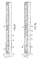
- FIGS. 1 a-b show the dishing phenomenon reference to the schematic cross-sectional views of multilayered structures
- FIGS. 2 a - 2 d are perspective descriptions of the method for producing optically planar surfaces, wherein first fill material is applied to first layer;
- FIG. 3 shows a profilometer trace after the etching of the second layer as disclosed in FIG. 2 c;
- FIG. 4 shows a profilometer trace after the CPM process of the second layer as disclosed in FIG. 2 c;
- FIG. 5 shows a profilometer trace after the CPM process without patterning as disclosed in FIG. 2 c;
- FIG. 6 is a perspective, partial cut-away view of a spatial light modulator with conformal grating electromechanical devices, showing two devices in a linear array;
- FIG. 7 is a top view of a spatial light modulator with conformal grating electromechanical devices, showing four individually operable devices in a linear array;
- FIGS. 8 a and 8 b are cross-sectional views through line 3 — 3 in FIG. 7, showing the operation of an conformal grating electromechanical device in an unactuated state and an actuated state, respectively;
- FIG. 9 a is a cross-sectional view through line 3 — 3 in FIG. 7 illustrating the layer structure prior to any patterning;
- FIG. 9 b is a cross-sectional view through line 3 — 3 in FIG. 7 illustrating patterning of the active region to form channels and intermediate supports;
- FIG. 9 c is a cross-sectional view through line 3 — 3 in FIG. 7 illustrating deposition of a sacrificial layer
- FIG. 9 d is a cross-sectional view through line 3 — 3 in FIG. 7 illustrating patterning of the sacrificial layer
- FIG. 9 e is a cross-sectional view through line 3 — 3 in FIG. 7 illustrating planarizing of the sacrificial layer
- FIG. 9 f is a cross-sectional view through line 3 — 3 in FIG. 7 illustrating deposition of a ribbon layer and a reflective and conductive layer;
- FIG. 9 g is a cross-sectional view through line 3 — 3 in FIG. 7 illustrating removal of the sacrificial layer after patterning elongated ribbon elements;
- FIG. 10 shows a profilometer trace after the etching of the sacrificial layer as disclosed in FIG. 9 d ;
- FIG. 11 shows a profilometer trace after the CMP process of the sacrificial layer as disclosed in FIG. 9 d.
- One class of electromechanical spatial light modulators has devices with a periodic sequence of reflective elements that form an electromechanical phase grating made of suspended micromechanical ribbon elements.
- a method of manufacturing such a device is described in U.S. Ser. No. 09/216,202 filed Dec. 18, 1998 by Hawkins et al., now granted as U.S. Pat. No. 6,238,581, to be issued May 29, 2001.
- the incident light beam is selectively reflected or diffracted into a number of discrete orders.
- one or more of these diffracted orders may be collected and used by the optical system.
- This method described by Hawkins et al. can be fabricated with CMOS-like processes on silicon.
- the device contains a plurality of spaced apart deformable ribbons that span a channel. Standoffs are patterned in the channel beneath the ribbons to minimize contact area and to obviate stiction between the ribbons and the substrate. Standoffs and also intermediate supports in the channel region will result in some types of topography that are transferred to the surface of the sacrificial layer. It is important that the sacrificial layer upon which the ribbons are deposited become optically planar by removal of any transferred topography. It is also important that the ribbons are securely attached to the end supports.
- the grating structure in the above device is defined by the patterning of the ribbon elements.
- a completely different class of electromechanical grating devices may be obtained by defining a grating structure in the supports below elongated ribbon elements, as disclosed by Kowarz in U.S. Ser. No. 09/491,354 filed Jan. 26, 2000. These devices function on the principle of a hidden grating. In the unactuated state, the grating structure is completely hidden from view and the device functions as a mirror. In the actuated state, the elongated ribbon elements deform to reveal the grating structure of the supports, thus generating a partially conformal diffraction grating.
- This conformal GEMS device contains elongated deformable ribbons spanning a channel containing a set of intermediate supports. Standoffs are patterned in the channel beneath the ribbons to minimize contact area and to obviate stiction between the ribbons and the substrate. It is important that the sacrificial layer upon which the ribbons are deposited becomes optically flat and coplanar with the intermediate supports. It is also important that the ribbons are securely attached to the end supports.
- FIGS. 2 a through 2 d are perspective descriptions of the inventive method for producing at least one optically planar surface. The following description is limited to a device which has a limited number of channels. It is clear for any skilled person that the inventive method is not limited solely to the embodiments disclosed in the specification.
- a first layer 200 is provided on a substrate 220 which has a channel 240 formed therein.
- the first layer 200 also includes a first layer top surface 260 .
- the channel 240 has a width W and a height H which is determined by the thickness of the first layer 200 .
- the channel 240 has a length which extends along the longitudinal axis of the substrate 220 .
- the longitudinal direction of the substrate 220 is marked by an arrow L—L.
- the channel 240 may include topography.
- a second layer 280 that conforms to the first layer 200 is deposited on top of the first layer 200 .
- the thickness of the second layer 280 is at least the height H of the channel 240 .
- the applied second layer 280 defines a conformed channel 300 at the same location as the channel 240 in the first layer 200 .
- the material used for the second layer 280 has to be different from the material of the first layer 200 .
- FIG. 2 c shows a first embodiment of the present invention.
- the selective removal of the second layer 280 is carried out by an appropriate patterning process which is, for example, followed by an etching step.
- the second layer 280 is removed from everywhere that is unprotected by a patterning or etch mask (not shown).
- the removal of the second layer 280 exposes the first layer top surface 260 .
- the patterning mask can be biased to provide overlap 320 to account for misalignment.
- the patterning of the second layer 280 is designed to minimize the width of these overlaps 320 in order to maximize the degree of planarization achieved with the chemical mechanical polishing step described below.
- the removal of the second layer outside of the channel 240 improves the uniformity of the planarization step described below. This removal process ensures good mechanical attachment of subsequent layers outside the channel 240 region.
- the second layer 280 can be a sacrificial layer that is completely removed upon completion of the device manufacturing process.
- the device (as shown in FIG. 2 c ) is subjected to a removing process for the remaining portion of second layer 280 .
- Chemical mechanical polishing methods are used to achieve the polished structure that includes a polished second layer top surface 340 .
- the second layer top surface 340 that fills the channel 240 is preferably polished to be optically planar. As is well known in the practice of optical engineering, this requires a surface planarity of less than about 200 Angstrom units at visible wavelengths.
- the thickness of the second layer 280 need not be the same as the first layer 200 .
- the thickness of the second layer 280 is closely related to the performance requirements of the micro-electromechanical, “MEMS” device.
- the surface of the second layer 280 need not be co-planar with the exterior of the device.
- FIGS. 3 — 5 show the improvement of surface quality achieved with the inventive method.
- the layer structure, used for the topography results, is comparable to the structure as shown in FIG. 2.
- a first layer 200 of thermally grown silicon dioxide is applied to the substrate 220 and etched to define a 50 ⁇ m wide channel 240 .
- a second layer 280 consisting of polysilicon is then deposited.
- a photoresist is patterned over the polysilicon to serve as an etch mask.
- the polysilicon is etched away defining a silicon dioxide surface 260 everywhere that is unprotected by the etch mask.
- the remaining polysilicon layer includes 2 microns of overlap 320 between the polysilicon and silicon dioxide around the channel 240 .
- FIG. 3 shows a surface profilometer trace of such a feature after the photoresist etch mask is removed.
- the substrates proceed through a CMP process step.
- the removal rate of the polysilicon is much greater than the silicon dioxide removal rate, therefore, little oxide is lost; less than 50 ⁇ .
- the removal rate of the polysilicon on the overlap regions 238 is higher than in the channel regions resulting in an optically planar polysilicon surface.
- the final thickness of the polysilicon second layer 280 is closely related to the performance requirements of the MEMS device.
- the thickness of the polysilicon second layer 280 need not be the same as the silicon dioxide first layer 200 .
- the height H2 of the polished polysilicon second layer top surface 340 need not be the same as the height H1 of the silicon dioxide first layer top surface 260 .
- FIG. 4 shows the surface topography around a 50 ⁇ m wide channel after CMP. Without patterning the polysilicon first, heavy dishing results, effectively removing the polysilicon from the channel 30 as illustrated in FIG. 5 .
- the processing for both examples included Rodel SDE3000 slurry, Rodel IC1000 pad with a SubaIV subpad on a Strasbaugh 6DS-SP CMP tool.
- the CMP conditions included a table speed of 55 rpm, spindle speed of 50 rpm, down pressure of 3 PSI, and table temperature of 25° C. It is clear for a skilled person that variations and modifications of the CMP conditions exist.
- FIG. 6 shows a perspective, partial cut-away view of a spatial light modulator with electromechanical conformal grating devices, disclosing two side-by-side conformal grating devices, 5 a and 5 b , in an unactuated state.
- the grating devices 5 a and 5 b are formed on top of a substrate 10 , that is covered by a bottom conductive layer 12 which acts as an electrode to actuate the devices.
- a dielectric protective layer 14 covers the bottom conductive layer 12 .
- a standoff layer 16 is formed which is followed by a spacer layer 18 .
- a ribbon layer 20 is formed which is covered by a reflective layer 22 .
- Each of the two devices 5 a and 5 b has an associated elongated ribbon element 23 a and 23 b , respectively, patterned from the reflective and conductive layer 22 and the ribbon layer 20 .
- the elongated ribbon elements 23 a and 23 b are supported by end supports 24 a and 24 b , that were formed from the spacer layer 18 , and by one or more intermediate supports 27 .
- end supports 24 a and 24 b that were formed from the spacer layer 18 , and by one or more intermediate supports 27 .
- three intermediate supports 27 are shown. These intermediate supports 27 are uniformly separated in order to form four equal-width channels 25 .
- the intermediate supports 27 form a grating structure, for the MEMS device, that is preferably completely hidden from view in an unactuated state and that causes the device to function as a mirror.
- the elongated ribbon elements of the MEMS device deform to reveal the grating structure of the intermediate supports 27 , thus generating a partially conformal diffraction grating. It is preferable that the elongated ribbon elements 23 a and 23 b are directly adhered to the end supports and directly adhered to the intermediate supports 27 . However, a small gap may actually exist between the intermediate supports 27 and the elongated ribbon elements 23 a and 23 b .
- the end supports 24 a and 24 b are not otherwise defined, other than at their edges that face the channels 25 .
- a plurality of square standoffs 29 is patterned at the bottom of the channels 25 from the standoff layer 16 . These standoffs 29 reduce the possibility of the ribbon elements sticking when actuated.
- the standoffs may also be patterned in shapes other than square, for example, rectangular or round.
- FIG. 7 A top view of a four-device linear array of conformal grating devices 5 a , 5 b , 5 c and 5 d is shown in FIG. 7 .
- the elongated ribbon elements 23 a , 23 b , 23 c , and 23 d are depicted partially removed over the portion of the diagram below the line 2 — 2 in order to show the underlying structure.
- the intermediate supports 27 must be completely hidden below the elongated ribbon elements 23 a , 23 b , 23 c and 23 d . Therefore, when viewed from the top, the intermediate supports must not be visible in the gaps 28 between the conformal grating devices 5 a - 5 d .
- each of the conformal grating devices has three intermediate supports 27 with four equal-width channels 25 .
- the active region 8 is the portion of the device where the electromechanical actuation takes place and contains the channels 25 , the intermediate supports 27 and the end supports 24 a and 24 b.
- the elongated ribbon elements 23 a - 23 d are mechanically and electrically isolated from one another, thus allowing independent operation of the four conformal grating devices 5 a - 5 d .
- the bottom conductive layer 12 of FIG. 6 can be common to all of the devices.
- FIG. 8 a is a side view, through line 3 — 3 of FIG. 7, of two channels 25 of the conformal grating device 5 b in the unactuated state.
- FIG. 8 b shows the same view of the actuated state.
- an attractive electrostatic force is produced by applying a voltage difference between the bottom conductive layer 12 and the conducting layer 22 of the elongated ribbon element 23 b .
- the unactuated state see FIG. 8 a
- it is important that the ribbon element 23 b is suspended flat between the intermediate supports 27 and the end supports 24 a and 24 b .
- an incident light beam 30 is primarily reflected 32 into the mirror direction.
- FIG. 8 b shows the device in the fully actuated state with the elongated ribbon element 23 b in contact with the standoffs 29 .
- the height difference between the bottom of element 23 b and the top of the standoffs 29 is chosen to be approximately 1 ⁇ 4 Of the wavelength ⁇ of the incident light. The optimum height depends on the specific shape of the actuated device. Preferably, the height defines the thickness of a sacrificial layer's final composition prior to depositing subsequent layers upon it.
- the incident light beam 30 is primarily diffracted into the +1st order 35 a and ⁇ 1st order 35 b , with additional light diffracted into the +2nd order 36 a and ⁇ 2nd order 36 b .
- a small amount of light is diffracted into even higher orders and some is reflected.
- the angle ⁇ m between the incident beam and the mth order diffracted beam is given by
- One or more of the diffracted orders can be collected and used by the optical system, depending on the application.
- the forces contributing to tensile stress and bending restore the ribbon element 23 b to its original unactuated state.
- This example of a spatial light modulator with electromechanical conformal grating is a preferred embodiment for use of the present invention to provide optically planar surfaces.
- the present invention is applicable to other electromechanical devices requiring an optically planar surface over topography.
- FIGS. 9 a - 9 g The fabrication sequence for making a conformal electromechanical grating device is illustrated in FIGS. 9 a - 9 g .
- the device is built upon a substrate 10 , covered by a bottom conductive layer 12 , and a protective layer 14 on top of the bottom conductive layer 12 .
- a standoff layer 16 is deposited followed by a spacer layer 18 .
- FIG. 9 b a cross-sectional view along line 3 — 3 indicated in FIG. 7, illustrates etching of the channels 25 to form the intermediate supports 27 .
- the standoff layer 16 is then patterned using photolithographic processing and etching methods to produce the standoffs 29 , as illustrated in FIG. 9 b .
- the standoffs 29 act as mechanical stops for the actuation of the conformal grating device.
- FIG. 9 c a cross-sectional view along line 3 — 3 indicated in FIG. 7, illustrates the deposition of a sacrificial layer 19 .
- a conformal sacrificial layer 19 is deposited to a thickness greater than the sum of the thickness of the standoff layer 16 and the spacer layer 18 .
- the material for the sacrificial layer 19 is different from the spacer layer 18 and is selected from the group consisting of silicon oxide, silicon nitride, polysilicon, doped-polysilicon, silicon-germanium alloys and polyimide.
- the sacrificial layer 19 is polysilicon deposited by chemical vapor deposition.
- FIG. 9 d a cross-sectional view along line 3 — 3 indicated in FIG. 7, illustrates the patterning of the sacrificial layer 19 .
- the patterning of the sacrificial layer 19 is carried out using standard photolithographic processing and a mask (not shown), which is the reverse of the mask used to etch the spacer layer 18 , defining the active region 8 where the channels 25 and intermediate supports 27 are located.
- the reversal mask (not shown) can be biased to provide overlap 21 to account for misalignment.
- the sacrificial layer is then completely removed from the areas defined by the reversal mask.
- the patterning of the sacrificial layer is designed to minimize the width of overlaps 21 in order to maximize the degree of planarization achieved with the chemical mechanical polishing step described below.
- the removal of the sacrificial layer outside of the active region 8 improves the uniformity of the planarization step described below. This removal process also ensures a good mechanical attachment or adhesion of the elongated ribbon elements 23 a - 23 d to the intermediate supports 27 and the end supports 24 a and 25 b (not shown in FIG. 9 d ).
- FIG. 9 e a cross-sectional view along line 3 — 3 indicated in FIG. 7, illustrates the planarization of the sacrificial layer 19 .
- Chemical mechanical polishing methods are used to achieve the polished structure.
- the polished surface of sacrificial layer 19 filling the channels 25 is preferably polished to be optically planar with the top surface of the intermediate supports 27 , but need not have optical planarity with end supports 24 a and 24 b .
- One reason for the requirement of optical planarity for the intermediate supports 27 and not the end supports 24 a and 24 b is because the intermediate supports 27 are critically functional to the optical efficiency of the device. In other words, the elongated ribbon element 23 b deforms around the intermediate supports 27 to produce a partially conformal grating having period ⁇ .
- FIG. 9 f is a cross-sectional view, along line 3 — 3 indicated in FIG. 7, and illustrates deposition of the ribbon layer 20 and the reflective and conductive layer 22 .
- the ribbon layer 20 is deposited on top of the optically planar sacrificial layer 19 and intermediate supports 27 , thereby covering the entire active region 8 of the device.
- Silicon nitride is a well-suited material for the ribbon layer 20 and can be patterned to provide the mechanical structure. Silicon nitride's material properties are well suited for the application because of the intrinsic and controllable tensile stress during the deposition process.
- the reflective and conductive layer 22 deposited atop the ribbon layer 20 requires good electrical conducting properties.
- the elongated ribbon elements 23 a - 23 d are patterned from the ribbon layer 20 and the reflective and conductive layer 22 using photolithographic processing and etching. This etching process defines the top-view geometry of the elongated ribbon elements 23 a - 23 d as shown in FIGS. 6 and 7.
- FIG. 9 g a cross-sectional view along line 3 — 3 indicated in FIG. 7, illustrates the removal of the sacrificial layer 19 from within the active region 8 to form channels 25 and intermediate supports 27 .
- the sacrificial layer 19 is polysilicon that can be selectively removed with dry etching methods to yield the cross-sectional view illustrated in FIG. 9 g .
- the etchant has access to the sacrificial layer 19 through the gaps 28 as shown in FIG. 7 between the elongated ribbon elements 23 a - 23 d .
- the complete removal of the sacrificial layer 19 is the final step required to produce operational conformal grating devices 5 a - 5 d .
- the devices can be actuated to operate as described earlier. More importantly, after completely removing the sacrificial layer 19 , the elongated ribbon elements 23 a - 23 d remain optically planar on both their bottom and top surfaces subject to the ribbon layer 20 having been deposited with uniform thickness and uniform tensile stress. Optically planar free-standing structures may also be produced with a similar method or process. One should note that an optical device may be in direct contact with support structures.
- FIGS. 10-11 illustrate the surface quality achieved with the inventive method.
- the layer structure, used for the topography results, is comparable to the structure as shown in FIGS. 9 a - 9 e .
- FIG. 10 shows a surface profilometer trace after the sacrificial layer 19 has been patterned and the etch mask removed.
- the end supports 24 a and 24 b are clear of any sacrificial layer 19 ; in contrast, the sacrificial layer 19 covers the intermediate supports 27 and channel 25 .
- the period between intermediate supports 27 is 25 microns.
- the intermediate supports 27 are 2 microns wide.
- the sacrificial layer 19 has been polished to a planar surface that is not co-planar with the end supports 24 a and 24 b , but is optically planar to the intermediate support 27 and channel regions 25 of the device 5 a .
- the surface of the sacrificial layer 19 is within 200 ⁇ of the oxide surface 16 with a planarity of less than 50 ⁇
Abstract
Description
Claims (30)
Priority Applications (1)
| Application Number | Priority Date | Filing Date | Title |
|---|---|---|---|
| US09/867,928 US6426237B2 (en) | 1998-12-18 | 2001-05-30 | Method for producing optically planar surfaces for micro-electromechanical system devices |
Applications Claiming Priority (2)
| Application Number | Priority Date | Filing Date | Title |
|---|---|---|---|
| US09/215,973 US6284560B1 (en) | 1998-12-18 | 1998-12-18 | Method for producing co-planar surface structures |
| US09/867,928 US6426237B2 (en) | 1998-12-18 | 2001-05-30 | Method for producing optically planar surfaces for micro-electromechanical system devices |
Related Parent Applications (1)
| Application Number | Title | Priority Date | Filing Date |
|---|---|---|---|
| US09/215,973 Continuation-In-Part US6284560B1 (en) | 1998-12-18 | 1998-12-18 | Method for producing co-planar surface structures |
Publications (2)
| Publication Number | Publication Date |
|---|---|
| US20010029058A1 US20010029058A1 (en) | 2001-10-11 |
| US6426237B2 true US6426237B2 (en) | 2002-07-30 |
Family
ID=22805139
Family Applications (2)
| Application Number | Title | Priority Date | Filing Date |
|---|---|---|---|
| US09/215,973 Expired - Lifetime US6284560B1 (en) | 1998-12-18 | 1998-12-18 | Method for producing co-planar surface structures |
| US09/867,928 Expired - Lifetime US6426237B2 (en) | 1998-12-18 | 2001-05-30 | Method for producing optically planar surfaces for micro-electromechanical system devices |
Family Applications Before (1)
| Application Number | Title | Priority Date | Filing Date |
|---|---|---|---|
| US09/215,973 Expired - Lifetime US6284560B1 (en) | 1998-12-18 | 1998-12-18 | Method for producing co-planar surface structures |
Country Status (4)
| Country | Link |
|---|---|
| US (2) | US6284560B1 (en) |
| EP (1) | EP1016620B1 (en) |
| JP (1) | JP4588147B2 (en) |
| DE (1) | DE69909727T2 (en) |
Cited By (3)
| Publication number | Priority date | Publication date | Assignee | Title |
|---|---|---|---|---|
| US20040002192A1 (en) * | 2002-05-16 | 2004-01-01 | Stmicroelectronics S.R.L. | Method for manufacturing non-volatile memory device |
| US20050184836A1 (en) * | 2004-02-20 | 2005-08-25 | Chia-Shing Chou | Microelectromechanical device having a common ground plane layer and a set of contact teeth and method for making the same |
| US7655996B1 (en) | 2005-02-03 | 2010-02-02 | The United States Of America As Represented By The Secretary Of The Army | MEMS structure support and release mechanism |
Families Citing this family (24)
| Publication number | Priority date | Publication date | Assignee | Title |
|---|---|---|---|---|
| US7297471B1 (en) | 2003-04-15 | 2007-11-20 | Idc, Llc | Method for manufacturing an array of interferometric modulators |
| US5704553A (en) * | 1995-10-30 | 1998-01-06 | Wieczorek; David P. | Compact injector armature valve assembly |
| KR100307630B1 (en) * | 1998-12-30 | 2001-09-28 | 윤종용 | Alignment Mark, Alignment System and Alignment Method Using the Same |
| US6724125B2 (en) | 1999-03-30 | 2004-04-20 | Massachusetts Institute Of Technology | Methods and apparatus for diffractive optical processing using an actuatable structure |
| US20020167695A1 (en) * | 2001-03-02 | 2002-11-14 | Senturia Stephen D. | Methods and apparatus for diffractive optical processing using an actuatable structure |
| US7046410B2 (en) | 2001-10-11 | 2006-05-16 | Polychromix, Inc. | Actuatable diffractive optical processor |
| US6794119B2 (en) * | 2002-02-12 | 2004-09-21 | Iridigm Display Corporation | Method for fabricating a structure for a microelectromechanical systems (MEMS) device |
| US7781850B2 (en) | 2002-09-20 | 2010-08-24 | Qualcomm Mems Technologies, Inc. | Controlling electromechanical behavior of structures within a microelectromechanical systems device |
| TW570896B (en) | 2003-05-26 | 2004-01-11 | Prime View Int Co Ltd | A method for fabricating an interference display cell |
| TW593126B (en) * | 2003-09-30 | 2004-06-21 | Prime View Int Co Ltd | A structure of a micro electro mechanical system and manufacturing the same |
| JP4377740B2 (en) * | 2004-04-28 | 2009-12-02 | 株式会社東芝 | Piezoelectric drive type MEMS element and mobile communication device having this piezoelectric drive type MEMS element |
| US7684104B2 (en) | 2004-09-27 | 2010-03-23 | Idc, Llc | MEMS using filler material and method |
| WO2007014022A1 (en) * | 2005-07-22 | 2007-02-01 | Qualcomm Incorporated | Mems devices having support structures and methods of fabricating the same |
| KR20080040715A (en) | 2005-07-22 | 2008-05-08 | 콸콤 인코포레이티드 | Support structure for mems device and methods therefor |
| EP2495212A3 (en) | 2005-07-22 | 2012-10-31 | QUALCOMM MEMS Technologies, Inc. | Mems devices having support structures and methods of fabricating the same |
| US7795061B2 (en) | 2005-12-29 | 2010-09-14 | Qualcomm Mems Technologies, Inc. | Method of creating MEMS device cavities by a non-etching process |
| US20070194239A1 (en) | 2006-01-31 | 2007-08-23 | Mcallister Abraham | Apparatus and method providing a hand-held spectrometer |
| US7711239B2 (en) | 2006-04-19 | 2010-05-04 | Qualcomm Mems Technologies, Inc. | Microelectromechanical device and method utilizing nanoparticles |
| JP4327183B2 (en) * | 2006-07-31 | 2009-09-09 | 株式会社日立製作所 | High pressure fuel pump control device for internal combustion engine |
| US7763546B2 (en) | 2006-08-02 | 2010-07-27 | Qualcomm Mems Technologies, Inc. | Methods for reducing surface charges during the manufacture of microelectromechanical systems devices |
| US7719752B2 (en) | 2007-05-11 | 2010-05-18 | Qualcomm Mems Technologies, Inc. | MEMS structures, methods of fabricating MEMS components on separate substrates and assembly of same |
| US8068268B2 (en) | 2007-07-03 | 2011-11-29 | Qualcomm Mems Technologies, Inc. | MEMS devices having improved uniformity and methods for making them |
| CN102858681B (en) * | 2010-03-01 | 2015-11-25 | 卡文迪什动力有限公司 | For the cmp handling process of MEMS |
| US8659816B2 (en) | 2011-04-25 | 2014-02-25 | Qualcomm Mems Technologies, Inc. | Mechanical layer and methods of making the same |
Citations (24)
| Publication number | Priority date | Publication date | Assignee | Title |
|---|---|---|---|---|
| FR2599892A1 (en) | 1986-06-10 | 1987-12-11 | Schiltz Andre | Method of flattening a semiconductor substrate coated with a dielectric layer |
| US4789648A (en) | 1985-10-28 | 1988-12-06 | International Business Machines Corporation | Method for producing coplanar multi-level metal/insulator films on a substrate and for forming patterned conductive lines simultaneously with stud vias |
| US4944836A (en) | 1985-10-28 | 1990-07-31 | International Business Machines Corporation | Chem-mech polishing method for producing coplanar metal/insulator films on a substrate |
| US4954142A (en) | 1989-03-07 | 1990-09-04 | International Business Machines Corporation | Method of chemical-mechanical polishing an electronic component substrate and polishing slurry therefor |
| US5173439A (en) | 1989-10-25 | 1992-12-22 | International Business Machines Corporation | Forming wide dielectric-filled isolation trenches in semi-conductors |
| US5311360A (en) | 1992-04-28 | 1994-05-10 | The Board Of Trustees Of The Leland Stanford, Junior University | Method and apparatus for modulating a light beam |
| EP0670591A2 (en) | 1994-03-04 | 1995-09-06 | Motorola, Inc. | Method for chemical mechanical polishing a semiconductor device using slurry |
| US5663107A (en) | 1994-12-22 | 1997-09-02 | Siemens Aktiengesellschaft | Global planarization using self aligned polishing or spacer technique and isotropic etch process |
| US5721172A (en) | 1996-12-02 | 1998-02-24 | Taiwan Semiconductor Manufacturing Company, Ltd. | Self-aligned polish stop layer hard masking method for forming planarized aperture fill layers |
| US5804084A (en) | 1996-10-11 | 1998-09-08 | Sandia Corporation | Use of chemical mechanical polishing in micromachining |
| US5899713A (en) | 1997-10-28 | 1999-05-04 | International Business Machines Corporation | Method of making NVRAM cell with planar control gate |
| US5904558A (en) | 1996-02-16 | 1999-05-18 | Nec Corporation | Fabrication process of semiconductor device |
| US5923993A (en) | 1997-12-17 | 1999-07-13 | Advanced Micro Devices | Method for fabricating dishing free shallow isolation trenches |
| US5948698A (en) | 1996-10-15 | 1999-09-07 | Kabushiki Kaisha Toshiba | Manufacturing method of semiconductor device using chemical mechanical polishing |
| US5948700A (en) | 1996-05-20 | 1999-09-07 | Chartered Semiconductor Manufacturing Ltd. | Method of planarization of an intermetal dielectric layer using chemical mechanical polishing |
| US5958795A (en) | 1998-04-18 | 1999-09-28 | United Microelectronics Corp. | Chemical-mechanical polishing for shallow trench isolation |
| US5976982A (en) | 1997-06-27 | 1999-11-02 | Siemens Aktiengesellschaft | Methods for protecting device components from chemical mechanical polish induced defects |
| US6001730A (en) | 1997-10-20 | 1999-12-14 | Motorola, Inc. | Chemical mechanical polishing (CMP) slurry for polishing copper interconnects which use tantalum-based barrier layers |
| US6004653A (en) | 1997-02-18 | 1999-12-21 | Winbond Electronics Corp. | Planarization process by applying a polish-differentiating technique utilizing an ultraviolet-light sensitive organic oxide layer |
| US6017803A (en) | 1998-06-24 | 2000-01-25 | Chartered Semiconductor Manufacturing, Ltd. | Method to prevent dishing in chemical mechanical polishing |
| US6020265A (en) | 1998-05-26 | 2000-02-01 | Worldwide Semiconductor Manufacturing Corporation | Method for forming a planar intermetal dielectric layer |
| US6022788A (en) | 1997-12-23 | 2000-02-08 | Stmicroelectronics, Inc. | Method of forming an integrated circuit having spacer after shallow trench fill and integrated circuit formed thereby |
| US6033961A (en) | 1998-04-30 | 2000-03-07 | Hewlett-Packard Company | Isolation trench fabrication process |
| US6048771A (en) | 1998-04-27 | 2000-04-11 | United Microelectronics Corp. | Shallow trench isolation technique |
Family Cites Families (4)
| Publication number | Priority date | Publication date | Assignee | Title |
|---|---|---|---|---|
| US602265A (en) * | 1898-04-12 | Cotton-opener | ||
| EP0424608B1 (en) * | 1989-10-25 | 1993-12-01 | International Business Machines Corporation | Forming wide dielectric filled isolation trenches in semiconductors |
| US5988713A (en) * | 1996-09-13 | 1999-11-23 | Daikyo Co., Ltd. | Bumper reinforcement |
| US6093631A (en) * | 1998-01-15 | 2000-07-25 | International Business Machines Corporation | Dummy patterns for aluminum chemical polishing (CMP) |
-
1998
- 1998-12-18 US US09/215,973 patent/US6284560B1/en not_active Expired - Lifetime
-
1999
- 1999-12-09 EP EP99204209A patent/EP1016620B1/en not_active Expired - Lifetime
- 1999-12-09 DE DE69909727T patent/DE69909727T2/en not_active Expired - Lifetime
- 1999-12-16 JP JP35680299A patent/JP4588147B2/en not_active Expired - Fee Related
-
2001
- 2001-05-30 US US09/867,928 patent/US6426237B2/en not_active Expired - Lifetime
Patent Citations (24)
| Publication number | Priority date | Publication date | Assignee | Title |
|---|---|---|---|---|
| US4789648A (en) | 1985-10-28 | 1988-12-06 | International Business Machines Corporation | Method for producing coplanar multi-level metal/insulator films on a substrate and for forming patterned conductive lines simultaneously with stud vias |
| US4944836A (en) | 1985-10-28 | 1990-07-31 | International Business Machines Corporation | Chem-mech polishing method for producing coplanar metal/insulator films on a substrate |
| FR2599892A1 (en) | 1986-06-10 | 1987-12-11 | Schiltz Andre | Method of flattening a semiconductor substrate coated with a dielectric layer |
| US4954142A (en) | 1989-03-07 | 1990-09-04 | International Business Machines Corporation | Method of chemical-mechanical polishing an electronic component substrate and polishing slurry therefor |
| US5173439A (en) | 1989-10-25 | 1992-12-22 | International Business Machines Corporation | Forming wide dielectric-filled isolation trenches in semi-conductors |
| US5311360A (en) | 1992-04-28 | 1994-05-10 | The Board Of Trustees Of The Leland Stanford, Junior University | Method and apparatus for modulating a light beam |
| EP0670591A2 (en) | 1994-03-04 | 1995-09-06 | Motorola, Inc. | Method for chemical mechanical polishing a semiconductor device using slurry |
| US5663107A (en) | 1994-12-22 | 1997-09-02 | Siemens Aktiengesellschaft | Global planarization using self aligned polishing or spacer technique and isotropic etch process |
| US5904558A (en) | 1996-02-16 | 1999-05-18 | Nec Corporation | Fabrication process of semiconductor device |
| US5948700A (en) | 1996-05-20 | 1999-09-07 | Chartered Semiconductor Manufacturing Ltd. | Method of planarization of an intermetal dielectric layer using chemical mechanical polishing |
| US5804084A (en) | 1996-10-11 | 1998-09-08 | Sandia Corporation | Use of chemical mechanical polishing in micromachining |
| US5948698A (en) | 1996-10-15 | 1999-09-07 | Kabushiki Kaisha Toshiba | Manufacturing method of semiconductor device using chemical mechanical polishing |
| US5721172A (en) | 1996-12-02 | 1998-02-24 | Taiwan Semiconductor Manufacturing Company, Ltd. | Self-aligned polish stop layer hard masking method for forming planarized aperture fill layers |
| US6004653A (en) | 1997-02-18 | 1999-12-21 | Winbond Electronics Corp. | Planarization process by applying a polish-differentiating technique utilizing an ultraviolet-light sensitive organic oxide layer |
| US5976982A (en) | 1997-06-27 | 1999-11-02 | Siemens Aktiengesellschaft | Methods for protecting device components from chemical mechanical polish induced defects |
| US6001730A (en) | 1997-10-20 | 1999-12-14 | Motorola, Inc. | Chemical mechanical polishing (CMP) slurry for polishing copper interconnects which use tantalum-based barrier layers |
| US5899713A (en) | 1997-10-28 | 1999-05-04 | International Business Machines Corporation | Method of making NVRAM cell with planar control gate |
| US5923993A (en) | 1997-12-17 | 1999-07-13 | Advanced Micro Devices | Method for fabricating dishing free shallow isolation trenches |
| US6022788A (en) | 1997-12-23 | 2000-02-08 | Stmicroelectronics, Inc. | Method of forming an integrated circuit having spacer after shallow trench fill and integrated circuit formed thereby |
| US5958795A (en) | 1998-04-18 | 1999-09-28 | United Microelectronics Corp. | Chemical-mechanical polishing for shallow trench isolation |
| US6048771A (en) | 1998-04-27 | 2000-04-11 | United Microelectronics Corp. | Shallow trench isolation technique |
| US6033961A (en) | 1998-04-30 | 2000-03-07 | Hewlett-Packard Company | Isolation trench fabrication process |
| US6020265A (en) | 1998-05-26 | 2000-02-01 | Worldwide Semiconductor Manufacturing Corporation | Method for forming a planar intermetal dielectric layer |
| US6017803A (en) | 1998-06-24 | 2000-01-25 | Chartered Semiconductor Manufacturing, Ltd. | Method to prevent dishing in chemical mechanical polishing |
Non-Patent Citations (3)
| Title |
|---|
| Roh et al., Easily Manufacturable Shallow Trench Isolation for Gigabit Dynamic Random Access Memory, Japanese Journal Appl. Phys., vol. 35, 1996, pp. 4618-4623. |
| U.S. application No. 09/216,202, Hawkins et al., filed Dec. 18, 1998, now granted as US Patent 6,238,581, to be issued May 29, 2001. |
| U.S. application No. 09/491,354, Kowarz, filed Jan. 26, 2000, now issued as US 6307663. |
Cited By (5)
| Publication number | Priority date | Publication date | Assignee | Title |
|---|---|---|---|---|
| US20040002192A1 (en) * | 2002-05-16 | 2004-01-01 | Stmicroelectronics S.R.L. | Method for manufacturing non-volatile memory device |
| US6812098B2 (en) * | 2002-05-16 | 2004-11-02 | Stmicroelectronics S.R.L. | Method for manufacturing non-volatile memory device |
| US20050184836A1 (en) * | 2004-02-20 | 2005-08-25 | Chia-Shing Chou | Microelectromechanical device having a common ground plane layer and a set of contact teeth and method for making the same |
| US7101724B2 (en) * | 2004-02-20 | 2006-09-05 | Wireless Mems, Inc. | Method of fabricating semiconductor devices employing at least one modulation doped quantum well structure and one or more etch stop layers for accurate contact formation |
| US7655996B1 (en) | 2005-02-03 | 2010-02-02 | The United States Of America As Represented By The Secretary Of The Army | MEMS structure support and release mechanism |
Also Published As
| Publication number | Publication date |
|---|---|
| EP1016620A2 (en) | 2000-07-05 |
| US6284560B1 (en) | 2001-09-04 |
| JP2000176899A (en) | 2000-06-27 |
| JP4588147B2 (en) | 2010-11-24 |
| EP1016620B1 (en) | 2003-07-23 |
| DE69909727T2 (en) | 2004-04-15 |
| EP1016620A3 (en) | 2001-01-17 |
| US20010029058A1 (en) | 2001-10-11 |
| DE69909727D1 (en) | 2003-08-28 |
Similar Documents
| Publication | Publication Date | Title |
|---|---|---|
| US6426237B2 (en) | Method for producing optically planar surfaces for micro-electromechanical system devices | |
| US6663788B2 (en) | Method for manufacturing a mechanical conformal grating device | |
| US6238581B1 (en) | Process for manufacturing an electro-mechanical grating device | |
| EP0830629B1 (en) | A method of making and an apparatus for a flat diffraction grating light valve | |
| US6541831B2 (en) | Single crystal silicon micromirror and array | |
| US6813059B2 (en) | Reduced formation of asperities in contact micro-structures | |
| CN100380165C (en) | Micromirrors and off-diagonal hinge structures for micromirror arrays in projection displays | |
| US5262000A (en) | Method for making micromechanical switch | |
| US20070035838A1 (en) | High contrast grating light valve | |
| EP0667548A1 (en) | Micromechanical modulator | |
| WO2010077998A1 (en) | Method of fabricating an integrated device | |
| US7163872B2 (en) | Tunable-wavelength optical filter and method of manufacturing the same | |
| US6663790B2 (en) | Method for manufacturing a mechanical conformal grating device with improved contrast and lifetime | |
| EP1528038A1 (en) | Diffractive thin-film piezoelectric micromirror and method of producing the same | |
| US6712480B1 (en) | Controlled curvature of stressed micro-structures | |
| KR950005004A (en) | Optical path control device for projection image display device and manufacturing method thereof | |
| US20020126455A1 (en) | Tiled microelectromechanical device modules and fabrication methods | |
| KR100425686B1 (en) | Optical modulator and manufacturing method thereof | |
| JP4349548B2 (en) | Manufacturing method of light modulation device | |
| KR100465914B1 (en) | Micro-actuator fabrication method | |
| KR100217953B1 (en) | Manufacture of strip-type emitter of fed | |
| KR20200039568A (en) | Mirror device for an interferometer device, interferometer device, method for producing a mirror device for an interferometer device, and method for producing an interferometer device | |
| EP2211223A1 (en) | Method for generating a deflectable mirror structure and a micromirror device | |
| KR19990043440A (en) | Manufacturing method of thin film type optical path control device | |
| KR20000044208A (en) | Thin film micromirror array-actuated device and manufacturing method thereof |
Legal Events
| Date | Code | Title | Description |
|---|---|---|---|
| AS | Assignment |
Owner name: EASTMAN KODAK COMPANY, NEW YORK Free format text: ASSIGNMENT OF ASSIGNORS INTEREST;ASSIGNORS:JECH, JR., JOSEPH;LEBENS, JOHN A.;BRAZAS, JR., JOHN C.;AND OTHERS;REEL/FRAME:011883/0816;SIGNING DATES FROM 20010524 TO 20010525 |
|
| STCF | Information on status: patent grant |
Free format text: PATENTED CASE |
|
| FEPP | Fee payment procedure |
Free format text: PAYOR NUMBER ASSIGNED (ORIGINAL EVENT CODE: ASPN); ENTITY STATUS OF PATENT OWNER: LARGE ENTITY |
|
| FPAY | Fee payment |
Year of fee payment: 4 |
|
| FPAY | Fee payment |
Year of fee payment: 8 |
|
| AS | Assignment |
Owner name: CITICORP NORTH AMERICA, INC., AS AGENT, NEW YORK Free format text: SECURITY INTEREST;ASSIGNORS:EASTMAN KODAK COMPANY;PAKON, INC.;REEL/FRAME:028201/0420 Effective date: 20120215 |
|
| AS | Assignment |
Owner name: WILMINGTON TRUST, NATIONAL ASSOCIATION, AS AGENT, Free format text: PATENT SECURITY AGREEMENT;ASSIGNORS:EASTMAN KODAK COMPANY;PAKON, INC.;REEL/FRAME:030122/0235 Effective date: 20130322 Owner name: WILMINGTON TRUST, NATIONAL ASSOCIATION, AS AGENT, MINNESOTA Free format text: PATENT SECURITY AGREEMENT;ASSIGNORS:EASTMAN KODAK COMPANY;PAKON, INC.;REEL/FRAME:030122/0235 Effective date: 20130322 |
|
| AS | Assignment |
Owner name: BANK OF AMERICA N.A., AS AGENT, MASSACHUSETTS Free format text: INTELLECTUAL PROPERTY SECURITY AGREEMENT (ABL);ASSIGNORS:EASTMAN KODAK COMPANY;FAR EAST DEVELOPMENT LTD.;FPC INC.;AND OTHERS;REEL/FRAME:031162/0117 Effective date: 20130903 Owner name: BARCLAYS BANK PLC, AS ADMINISTRATIVE AGENT, NEW YORK Free format text: INTELLECTUAL PROPERTY SECURITY AGREEMENT (SECOND LIEN);ASSIGNORS:EASTMAN KODAK COMPANY;FAR EAST DEVELOPMENT LTD.;FPC INC.;AND OTHERS;REEL/FRAME:031159/0001 Effective date: 20130903 Owner name: JPMORGAN CHASE BANK, N.A., AS ADMINISTRATIVE, DELAWARE Free format text: INTELLECTUAL PROPERTY SECURITY AGREEMENT (FIRST LIEN);ASSIGNORS:EASTMAN KODAK COMPANY;FAR EAST DEVELOPMENT LTD.;FPC INC.;AND OTHERS;REEL/FRAME:031158/0001 Effective date: 20130903 Owner name: PAKON, INC., NEW YORK Free format text: RELEASE OF SECURITY INTEREST IN PATENTS;ASSIGNORS:CITICORP NORTH AMERICA, INC., AS SENIOR DIP AGENT;WILMINGTON TRUST, NATIONAL ASSOCIATION, AS JUNIOR DIP AGENT;REEL/FRAME:031157/0451 Effective date: 20130903 Owner name: EASTMAN KODAK COMPANY, NEW YORK Free format text: RELEASE OF SECURITY INTEREST IN PATENTS;ASSIGNORS:CITICORP NORTH AMERICA, INC., AS SENIOR DIP AGENT;WILMINGTON TRUST, NATIONAL ASSOCIATION, AS JUNIOR DIP AGENT;REEL/FRAME:031157/0451 Effective date: 20130903 Owner name: JPMORGAN CHASE BANK, N.A., AS ADMINISTRATIVE, DELA Free format text: INTELLECTUAL PROPERTY SECURITY AGREEMENT (FIRST LIEN);ASSIGNORS:EASTMAN KODAK COMPANY;FAR EAST DEVELOPMENT LTD.;FPC INC.;AND OTHERS;REEL/FRAME:031158/0001 Effective date: 20130903 Owner name: BARCLAYS BANK PLC, AS ADMINISTRATIVE AGENT, NEW YO Free format text: INTELLECTUAL PROPERTY SECURITY AGREEMENT (SECOND LIEN);ASSIGNORS:EASTMAN KODAK COMPANY;FAR EAST DEVELOPMENT LTD.;FPC INC.;AND OTHERS;REEL/FRAME:031159/0001 Effective date: 20130903 |
|
| FPAY | Fee payment |
Year of fee payment: 12 |
|
| AS | Assignment |
Owner name: KODAK PHILIPPINES, LTD., NEW YORK Free format text: RELEASE BY SECURED PARTY;ASSIGNOR:JP MORGAN CHASE BANK, N.A., AS ADMINISTRATIVE AGENT;REEL/FRAME:049814/0001 Effective date: 20190617 Owner name: QUALEX, INC., NEW YORK Free format text: RELEASE BY SECURED PARTY;ASSIGNOR:JP MORGAN CHASE BANK, N.A., AS ADMINISTRATIVE AGENT;REEL/FRAME:049814/0001 Effective date: 20190617 Owner name: PAKON, INC., NEW YORK Free format text: RELEASE BY SECURED PARTY;ASSIGNOR:JP MORGAN CHASE BANK, N.A., AS ADMINISTRATIVE AGENT;REEL/FRAME:049814/0001 Effective date: 20190617 Owner name: KODAK REALTY, INC., NEW YORK Free format text: RELEASE BY SECURED PARTY;ASSIGNOR:JP MORGAN CHASE BANK, N.A., AS ADMINISTRATIVE AGENT;REEL/FRAME:049814/0001 Effective date: 20190617 Owner name: LASER PACIFIC MEDIA CORPORATION, NEW YORK Free format text: RELEASE BY SECURED PARTY;ASSIGNOR:JP MORGAN CHASE BANK, N.A., AS ADMINISTRATIVE AGENT;REEL/FRAME:049814/0001 Effective date: 20190617 Owner name: KODAK PORTUGUESA LIMITED, NEW YORK Free format text: RELEASE BY SECURED PARTY;ASSIGNOR:JP MORGAN CHASE BANK, N.A., AS ADMINISTRATIVE AGENT;REEL/FRAME:049814/0001 Effective date: 20190617 Owner name: CREO MANUFACTURING AMERICA LLC, NEW YORK Free format text: RELEASE BY SECURED PARTY;ASSIGNOR:JP MORGAN CHASE BANK, N.A., AS ADMINISTRATIVE AGENT;REEL/FRAME:049814/0001 Effective date: 20190617 Owner name: FAR EAST DEVELOPMENT LTD., NEW YORK Free format text: RELEASE BY SECURED PARTY;ASSIGNOR:JP MORGAN CHASE BANK, N.A., AS ADMINISTRATIVE AGENT;REEL/FRAME:049814/0001 Effective date: 20190617 Owner name: KODAK IMAGING NETWORK, INC., NEW YORK Free format text: RELEASE BY SECURED PARTY;ASSIGNOR:JP MORGAN CHASE BANK, N.A., AS ADMINISTRATIVE AGENT;REEL/FRAME:049814/0001 Effective date: 20190617 Owner name: KODAK AVIATION LEASING LLC, NEW YORK Free format text: RELEASE BY SECURED PARTY;ASSIGNOR:JP MORGAN CHASE BANK, N.A., AS ADMINISTRATIVE AGENT;REEL/FRAME:049814/0001 Effective date: 20190617 Owner name: KODAK AMERICAS, LTD., NEW YORK Free format text: RELEASE BY SECURED PARTY;ASSIGNOR:JP MORGAN CHASE BANK, N.A., AS ADMINISTRATIVE AGENT;REEL/FRAME:049814/0001 Effective date: 20190617 Owner name: NPEC, INC., NEW YORK Free format text: RELEASE BY SECURED PARTY;ASSIGNOR:JP MORGAN CHASE BANK, N.A., AS ADMINISTRATIVE AGENT;REEL/FRAME:049814/0001 Effective date: 20190617 Owner name: KODAK (NEAR EAST), INC., NEW YORK Free format text: RELEASE BY SECURED PARTY;ASSIGNOR:JP MORGAN CHASE BANK, N.A., AS ADMINISTRATIVE AGENT;REEL/FRAME:049814/0001 Effective date: 20190617 Owner name: EASTMAN KODAK COMPANY, NEW YORK Free format text: RELEASE BY SECURED PARTY;ASSIGNOR:JP MORGAN CHASE BANK, N.A., AS ADMINISTRATIVE AGENT;REEL/FRAME:049814/0001 Effective date: 20190617 Owner name: FPC, INC., NEW YORK Free format text: RELEASE BY SECURED PARTY;ASSIGNOR:JP MORGAN CHASE BANK, N.A., AS ADMINISTRATIVE AGENT;REEL/FRAME:049814/0001 Effective date: 20190617 |
|
| AS | Assignment |
Owner name: NPEC INC., NEW YORK Free format text: RELEASE BY SECURED PARTY;ASSIGNOR:BARCLAYS BANK PLC;REEL/FRAME:052773/0001 Effective date: 20170202 Owner name: LASER PACIFIC MEDIA CORPORATION, NEW YORK Free format text: RELEASE BY SECURED PARTY;ASSIGNOR:BARCLAYS BANK PLC;REEL/FRAME:052773/0001 Effective date: 20170202 Owner name: QUALEX INC., NEW YORK Free format text: RELEASE BY SECURED PARTY;ASSIGNOR:BARCLAYS BANK PLC;REEL/FRAME:052773/0001 Effective date: 20170202 Owner name: KODAK REALTY INC., NEW YORK Free format text: RELEASE BY SECURED PARTY;ASSIGNOR:BARCLAYS BANK PLC;REEL/FRAME:052773/0001 Effective date: 20170202 Owner name: FAR EAST DEVELOPMENT LTD., NEW YORK Free format text: RELEASE BY SECURED PARTY;ASSIGNOR:BARCLAYS BANK PLC;REEL/FRAME:052773/0001 Effective date: 20170202 Owner name: EASTMAN KODAK COMPANY, NEW YORK Free format text: RELEASE BY SECURED PARTY;ASSIGNOR:BARCLAYS BANK PLC;REEL/FRAME:052773/0001 Effective date: 20170202 Owner name: FPC INC., NEW YORK Free format text: RELEASE BY SECURED PARTY;ASSIGNOR:BARCLAYS BANK PLC;REEL/FRAME:052773/0001 Effective date: 20170202 Owner name: KODAK AMERICAS LTD., NEW YORK Free format text: RELEASE BY SECURED PARTY;ASSIGNOR:BARCLAYS BANK PLC;REEL/FRAME:052773/0001 Effective date: 20170202 Owner name: KODAK (NEAR EAST) INC., NEW YORK Free format text: RELEASE BY SECURED PARTY;ASSIGNOR:BARCLAYS BANK PLC;REEL/FRAME:052773/0001 Effective date: 20170202 Owner name: KODAK PHILIPPINES LTD., NEW YORK Free format text: RELEASE BY SECURED PARTY;ASSIGNOR:BARCLAYS BANK PLC;REEL/FRAME:052773/0001 Effective date: 20170202 |