US6423241B1 - Ink jet print head and a method of producing the same - Google Patents
Ink jet print head and a method of producing the same Download PDFInfo
- Publication number
- US6423241B1 US6423241B1 US09/209,560 US20956098A US6423241B1 US 6423241 B1 US6423241 B1 US 6423241B1 US 20956098 A US20956098 A US 20956098A US 6423241 B1 US6423241 B1 US 6423241B1
- Authority
- US
- United States
- Prior art keywords
- photoresist
- ink
- photoresist mold
- mold
- barrier layer
- Prior art date
- Legal status (The legal status is an assumption and is not a legal conclusion. Google has not performed a legal analysis and makes no representation as to the accuracy of the status listed.)
- Expired - Fee Related
Links
- 238000000034 method Methods 0.000 title claims abstract description 57
- 229920002120 photoresistant polymer Polymers 0.000 claims abstract description 218
- 229910052751 metal Inorganic materials 0.000 claims abstract description 106
- 239000002184 metal Substances 0.000 claims abstract description 106
- 230000004888 barrier function Effects 0.000 claims abstract description 72
- 238000007747 plating Methods 0.000 claims abstract description 46
- 238000009736 wetting Methods 0.000 claims abstract description 13
- 238000009713 electroplating Methods 0.000 claims abstract description 5
- 238000007772 electroless plating Methods 0.000 claims abstract description 4
- 239000000758 substrate Substances 0.000 claims description 69
- 230000001678 irradiating effect Effects 0.000 claims description 16
- 238000005260 corrosion Methods 0.000 claims description 6
- 238000005530 etching Methods 0.000 claims description 6
- 239000011248 coating agent Substances 0.000 claims description 4
- 238000000576 coating method Methods 0.000 claims description 4
- 239000012530 fluid Substances 0.000 claims description 2
- 238000004519 manufacturing process Methods 0.000 abstract description 38
- 239000010410 layer Substances 0.000 description 119
- PXHVJJICTQNCMI-UHFFFAOYSA-N nickel Substances [Ni] PXHVJJICTQNCMI-UHFFFAOYSA-N 0.000 description 31
- 230000015572 biosynthetic process Effects 0.000 description 15
- 238000000059 patterning Methods 0.000 description 14
- 101000573637 Homo sapiens LRP chaperone MESD Proteins 0.000 description 8
- 102100026257 LRP chaperone MESD Human genes 0.000 description 8
- 239000011241 protective layer Substances 0.000 description 7
- CSCPPACGZOOCGX-UHFFFAOYSA-N Acetone Chemical compound CC(C)=O CSCPPACGZOOCGX-UHFFFAOYSA-N 0.000 description 6
- 239000000853 adhesive Substances 0.000 description 5
- 239000010931 gold Substances 0.000 description 4
- 229910052759 nickel Inorganic materials 0.000 description 4
- 238000005498 polishing Methods 0.000 description 4
- 239000010936 titanium Substances 0.000 description 4
- RTAQQCXQSZGOHL-UHFFFAOYSA-N Titanium Chemical compound [Ti] RTAQQCXQSZGOHL-UHFFFAOYSA-N 0.000 description 3
- PCHJSUWPFVWCPO-UHFFFAOYSA-N gold Chemical compound [Au] PCHJSUWPFVWCPO-UHFFFAOYSA-N 0.000 description 3
- 229910052737 gold Inorganic materials 0.000 description 3
- 238000010438 heat treatment Methods 0.000 description 3
- 239000003960 organic solvent Substances 0.000 description 3
- 229910052719 titanium Inorganic materials 0.000 description 3
- VYZAMTAEIAYCRO-UHFFFAOYSA-N Chromium Chemical compound [Cr] VYZAMTAEIAYCRO-UHFFFAOYSA-N 0.000 description 2
- 239000011651 chromium Substances 0.000 description 2
- 229910052804 chromium Inorganic materials 0.000 description 2
- 238000011161 development Methods 0.000 description 2
- 238000007641 inkjet printing Methods 0.000 description 2
- 238000000206 photolithography Methods 0.000 description 2
- 239000000126 substance Substances 0.000 description 2
- 239000010409 thin film Substances 0.000 description 2
- 241001070941 Castanea Species 0.000 description 1
- 235000014036 Castanea Nutrition 0.000 description 1
- 238000013459 approach Methods 0.000 description 1
- 238000010276 construction Methods 0.000 description 1
- 238000000151 deposition Methods 0.000 description 1
- 238000013461 design Methods 0.000 description 1
- 230000000694 effects Effects 0.000 description 1
- 239000003792 electrolyte Substances 0.000 description 1
- 239000011159 matrix material Substances 0.000 description 1
- 229920001721 polyimide Polymers 0.000 description 1
- 229920000642 polymer Polymers 0.000 description 1
- 238000007670 refining Methods 0.000 description 1
- 238000011160 research Methods 0.000 description 1
- 239000004065 semiconductor Substances 0.000 description 1
- 229910001220 stainless steel Inorganic materials 0.000 description 1
- 239000010935 stainless steel Substances 0.000 description 1
- 230000001131 transforming effect Effects 0.000 description 1
Images


Classifications
-
- B—PERFORMING OPERATIONS; TRANSPORTING
- B41—PRINTING; LINING MACHINES; TYPEWRITERS; STAMPS
- B41J—TYPEWRITERS; SELECTIVE PRINTING MECHANISMS, i.e. MECHANISMS PRINTING OTHERWISE THAN FROM A FORME; CORRECTION OF TYPOGRAPHICAL ERRORS
- B41J2/00—Typewriters or selective printing mechanisms characterised by the printing or marking process for which they are designed
- B41J2/005—Typewriters or selective printing mechanisms characterised by the printing or marking process for which they are designed characterised by bringing liquid or particles selectively into contact with a printing material
- B41J2/01—Ink jet
- B41J2/135—Nozzles
- B41J2/16—Production of nozzles
- B41J2/1621—Manufacturing processes
- B41J2/1626—Manufacturing processes etching
-
- B—PERFORMING OPERATIONS; TRANSPORTING
- B41—PRINTING; LINING MACHINES; TYPEWRITERS; STAMPS
- B41J—TYPEWRITERS; SELECTIVE PRINTING MECHANISMS, i.e. MECHANISMS PRINTING OTHERWISE THAN FROM A FORME; CORRECTION OF TYPOGRAPHICAL ERRORS
- B41J2/00—Typewriters or selective printing mechanisms characterised by the printing or marking process for which they are designed
- B41J2/005—Typewriters or selective printing mechanisms characterised by the printing or marking process for which they are designed characterised by bringing liquid or particles selectively into contact with a printing material
- B41J2/01—Ink jet
- B41J2/135—Nozzles
- B41J2/16—Production of nozzles
- B41J2/1601—Production of bubble jet print heads
- B41J2/1603—Production of bubble jet print heads of the front shooter type
-
- B—PERFORMING OPERATIONS; TRANSPORTING
- B41—PRINTING; LINING MACHINES; TYPEWRITERS; STAMPS
- B41J—TYPEWRITERS; SELECTIVE PRINTING MECHANISMS, i.e. MECHANISMS PRINTING OTHERWISE THAN FROM A FORME; CORRECTION OF TYPOGRAPHICAL ERRORS
- B41J2/00—Typewriters or selective printing mechanisms characterised by the printing or marking process for which they are designed
- B41J2/005—Typewriters or selective printing mechanisms characterised by the printing or marking process for which they are designed characterised by bringing liquid or particles selectively into contact with a printing material
- B41J2/01—Ink jet
- B41J2/135—Nozzles
- B41J2/16—Production of nozzles
- B41J2/1621—Manufacturing processes
- B41J2/1631—Manufacturing processes photolithography
-
- B—PERFORMING OPERATIONS; TRANSPORTING
- B41—PRINTING; LINING MACHINES; TYPEWRITERS; STAMPS
- B41J—TYPEWRITERS; SELECTIVE PRINTING MECHANISMS, i.e. MECHANISMS PRINTING OTHERWISE THAN FROM A FORME; CORRECTION OF TYPOGRAPHICAL ERRORS
- B41J2/00—Typewriters or selective printing mechanisms characterised by the printing or marking process for which they are designed
- B41J2/005—Typewriters or selective printing mechanisms characterised by the printing or marking process for which they are designed characterised by bringing liquid or particles selectively into contact with a printing material
- B41J2/01—Ink jet
- B41J2/135—Nozzles
- B41J2/16—Production of nozzles
- B41J2/1621—Manufacturing processes
- B41J2/1632—Manufacturing processes machining
-
- B—PERFORMING OPERATIONS; TRANSPORTING
- B41—PRINTING; LINING MACHINES; TYPEWRITERS; STAMPS
- B41J—TYPEWRITERS; SELECTIVE PRINTING MECHANISMS, i.e. MECHANISMS PRINTING OTHERWISE THAN FROM A FORME; CORRECTION OF TYPOGRAPHICAL ERRORS
- B41J2/00—Typewriters or selective printing mechanisms characterised by the printing or marking process for which they are designed
- B41J2/005—Typewriters or selective printing mechanisms characterised by the printing or marking process for which they are designed characterised by bringing liquid or particles selectively into contact with a printing material
- B41J2/01—Ink jet
- B41J2/135—Nozzles
- B41J2/16—Production of nozzles
- B41J2/1621—Manufacturing processes
- B41J2/1637—Manufacturing processes molding
- B41J2/1639—Manufacturing processes molding sacrificial molding
-
- B—PERFORMING OPERATIONS; TRANSPORTING
- B41—PRINTING; LINING MACHINES; TYPEWRITERS; STAMPS
- B41J—TYPEWRITERS; SELECTIVE PRINTING MECHANISMS, i.e. MECHANISMS PRINTING OTHERWISE THAN FROM A FORME; CORRECTION OF TYPOGRAPHICAL ERRORS
- B41J2/00—Typewriters or selective printing mechanisms characterised by the printing or marking process for which they are designed
- B41J2/005—Typewriters or selective printing mechanisms characterised by the printing or marking process for which they are designed characterised by bringing liquid or particles selectively into contact with a printing material
- B41J2/01—Ink jet
- B41J2/135—Nozzles
- B41J2/16—Production of nozzles
- B41J2/1621—Manufacturing processes
- B41J2/164—Manufacturing processes thin film formation
- B41J2/1643—Manufacturing processes thin film formation thin film formation by plating
Definitions
- the present invention relates to an ink jet print head including a plurality of ink ejecting orifices which are formed at a desired shape and a uniform size by only once using a plating technique of a metal, having an excellent productivity and a low manufacturing cost.
- the invention also relates to a method of producing the ink jet print head.
- an ink jet printer makes a light noise and shows an excellent resolution.
- the ink jet printer can provide a colorful printed matter at a low cost.
- the ink jet printer is relatively well developed and broadly sold as compared with a dot matrix printer or a laser printer in the field of a personal computer market.
- a manufacturing technique of a print head that is an important component of the ink jet printer makes rapid progress in the last ten years due to the development of a semiconductor manufacturing technique.
- a print head having about 300 nozzles for ejecting ink and capable of providing 600 dpi resolution can be produced as it is mounted to a disposable ink cartridge.
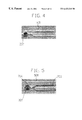
- FIGS. 15 and 16 show this thermal ink jet print head. That is, FIG. 15 is a sectional view of the thermal ink jet print head, and FIG. 16 is a perspective view of the ink jet print head shown in FIG. 15, showing the positions and the shapes of an ink channel, an ink cavity and an ink ejecting orifice.
- FIGS. 15 & 16 show this thermal ink jet print head. That is, FIG. 15 is a sectional view of the thermal ink jet print head, and FIG. 16 is a perspective view of the ink jet print head shown in FIG. 15, showing the positions and the shapes of an ink channel, an ink cavity and an ink ejecting orifice.
- ink approaches toward a front surface of a substrate 101 of an ink jet print head 100 through a first ink channel 102 from a rear surface of substrate 101 of ink jet print head 100 .
- the ink supplied through first ink channel 102 flows along a second ink channel 103 defined by a barrier layer 108 and a nozzle plate 109 , and then enters into an ink cavity 104 .
- the ink temporarily contained in ink cavity 104 is instantaneously heated by heat generated from a resistance element 106 disposed below a protective layer 105 .
- ink ejecting orifice 107 which is formed at a predetermined position above ink cavity 104 , by air bubbles generated in the ink due to the heat.
- barrier layer 108 and nozzle plate 109 are important factors capable of determining the whole flowing characteristic of the ink fluid. That is, barrier layer 108 and nozzle plate 109 have an effect upon a flow of the ink, an ejecting shape of the ink, a satellite characteristic and an ink ejecting frequency characteristic, etc. Therefore, a variety of researches in relation to the quality, the shape and the manufacturing methods of barrier layer 108 and nozzle plate 109 have been performed.
- the manufacturing methods of the ink jet print head in relation to the barrier layer and the nozzle plate can be classified into a method for manufacturing a hybrid ink jet print head and a method for manufacturing a monolithic ink jet print head.
- a substrate and a nozzle plate are separately produced and thereafter they are combined together using a certain adhesive agent.
- the nozzle plate is separately produced and thereafter it is aligned on the substrate on which a barrier layer made of polymer is laid. Under this state, the nozzle plate is attached to the substrate using the adhesive agent.
- the nozzle plate and the barrier layer are produced as one body, and thereafter they are aligned on the substrate. Under this state, they are attached to the substrate by using the adhesive agent.
- the barrier layer and the nozzle plate directly grow up on the substrate.
- a primary advantage of the method for manufacturing the monolithic ink jet print head over the method for manufacturing the hybrid ink jet print head is that it is unnecessary to have a mandrel made of stainless steel required to plate the nozzle plate. As a result, there are no subordinate steps required to separate the mandrel from the nozzle plate. Further, it is unnecessary to provide any adhesive agent consumed to attach the nozzle plate to the substrate. Thereby, there are no working steps and equipments for combining the nozzle plate and the substrate with each other using the adhesive agent. In addition, it is possible to elaborately align the substrate, the barrier layer and the nozzle plate with one another. Therefore, it is possible to reduce the manufacturing steps of the ink jet print head. Thereby, the manufacturing cost thereof is reduced and the productivity is enhanced. In addition, the method for manufacturing the monolithic ink jet print head is adapted to manufacture an ink jet print head for a high resolution, which necessitates an elaborate alignment.
- FIGS. 17A to 17 C illustrate schematically a sequence of manufacturing steps of a monolithic ink jet print head according to a prior art
- the sequence of manufacturing steps of the monolithic ink jet print head will be briefly explained with reference to FIGS. 17A to 17 C.
- a first seed metal layer 301 for plating a metal barrier layer is deposited on a substrate 101 in which a resistance element 106 and a protective layer 105 are formed.
- an upper surface of protective layer 105 is plated with titanium at a thickness of about 200 ⁇ to provide good adhesion.
- gold is deposited thereon at a thickness of about 2,000 ⁇ .
- first photoresist molds 302 , 303 are formed on first seed metal layer 301 by using photolithography technique.
- first photoresist molds 302 , 303 are etched with HF to provide an ink channel and an ink cavity. At this time, the height of first photoresist molds 302 , 303 is about 30 ⁇ 40 ⁇ m. This height is the same as that of the ink channel and the ink cavity.
- first photoresist molds 302 , 303 Following formation of first photoresist molds 302 , 303 on first seed metal layer 301 , a metal barrier layer 108 is deposited on first seed metal layer 301 by plating of Ni up to the height of first photoresist molds 302 , 303 . Thereafter, a second seed metal layer 304 for a secondary plating of a metal is deposited on metal barrier layer 108 and first photoresist molds 302 , 303 in accordance with the same forming method as that of first seed metal layer 301 .
- second photoresist mold 305 , second wetting layer 304 , first photoresist molds 302 , 303 and first wetting layer 301 which are located in barrier layer 108 and nozzle plate 109 , are etched with HF in sequence. Consequently, an ink ejecting orifice 107 , an ink cavity 104 and a second ink channel 103 are formed and thereby a passage allowing the ink to flow is created. Thereafter, in order to prevent barrier layer 108 and nozzle plate 109 from being corroded by the ink following along the passage, anti-corrosion plating is performed. As a result, barrier layer 108 and nozzle plate 109 are completely produced. Finally, a first ink channel 102 is formed in substrate 101 using electrolyte polishing, and thereby a print head 100 having a complete structure is manufactured.
- second photoresist mold 305 Following formation of metal nozzle plate 109 , second photoresist mold 305 , second seed metal layer 304 , first photoresist molds 302 , 303 and first seed metal layer 301 , which are located in barrier layer 108 and nozzle plate 109 , are etched with HF in sequence. Consequently, an ink ejecting orifice 107 , an ink cavity 104 and a second ink channel 105 are formed and thereby a passage allowing the ink to flow is created. Thereafter, in order to prevent barrier layer 108 and nozzle plate 109 from being corroded by the ink flowing along the passage, anti-corrosion plating is performed. As a result, barrier layer 108 and nozzle plate 109 are completely produced. Finally, a first ink channel 102 is formed in substrate 101 using the electrolytic polishing, and thereby a print head 100 having a complete structure is manufactured.
- metal barrier layer 108 consisted of Ni is deposited up to the height of first photoresist molds 302 , 303 , it is difficult to align the height of metal barrier layer 108 with that first photoresist molds 302 , 303 on a substrate having a wide area.
- the present invention is contrived to solve the foregoing problems. It is a first object of the present invention to provide a method of producing an ink jet print head including a plurality of ink ejecting orifices which are formed at a desired shape and a uniform size by only once using a plating technique of a metal, having an excellent productivity and a low manufacturing cost.
- the present invention provides a method of producing an ink jet print head, comprising the steps of:
- the method further comprises the step of (f) anti-corrosion plating an inner surface of the ink flowing passage in order to prevent the metal barrier layer from being corroded by the ink flowing along the ink flowing passage.
- the ink flowing passage includes an auxiliary ink channel, an ink cavity and an ink ejecting orifice, which are fluid-communicated with one another.
- the photoresist mold includes a first photoresist mold corresponding to the auxiliary ink channel and a second photoresist mold corresponding to the ink cavity.
- the photoresist mold includes a first photoresist mold corresponding to the auxiliary ink channel, a second photoresist mold corresponding to the ink cavity, and a third photoresist mold corresponding to the ink ejecting orifice.
- the step of (b) forming the photoresist mold comprising the steps of:
- step of (b) forming the photoresist mold comprising the steps of:
- an ink jet print head including a plurality of ink ejecting orifices which are distributed on a wide wafer and has a desired shape, a uniform size and a high sectional height, which are adapted to an optimum ejection of the ink.
- an ink jet print head comprising:
- a substrate having a resistance element for heating ink therein, a seed metal layer deposited on an upper surface thereof, and a main ink supplying passage allowing the ink supplied from an ink source to flow therethrough;
- a metal barrier layer having an ink ejecting orifice for ejecting the ink contained in an ink cavity out of the ink jet print head, the metal barrier layer upwardly extending from the seed metal layer, the metal barrier layer refining an auxiliary ink channel and the ink cavity with the aid of an upper surface of the substrate in order to flow the ink being introduced through the main ink supplying passage.
- the ink ejecting orifice has a circular shape, a triangular shape or a quadrangular shape.
- the ink channel, the ink cavity and the ink ejecting orifice capable of allowing the ink to flow can be formed.
- the metal plating is converged around the photoresist mold protruding as the shape of the ink ejecting orifice.
- the plurality of ink ejecting orifices formed on the wide wafer have the uniform size, the desired shape and the high sectional height which are adapted to the optimum ejection of the ink.
- FIGS. 1A to 3 illustrate schematically a sequence of manufacturing steps of an ink jet print head according to a preferred first embodiment of the present invention
- FIG. 4 is a scanning electron photomicrograph looked down on the ink jet print head according to the preferred first embodiment of the present invention.
- FIG. 5 is a scanning electron photomicrograph looked up the ink jet print head according to the preferred first embodiment of the present invention, under the state that a substrate of the ink jet print head is removed;
- FIGS. 6A to 8 illustrate schematically a sequence of manufacturing steps of an ink jet print head according to a preferred second embodiment of the present invention
- FIGS. 9A to 9 C illustrate schematically a sequence of patterning steps of a photoresist having a three-dimensional structure
- FIG. 10 is a graph showing relations between a variety of exposure rates of the ultraviolet rays and a developing characteristic of the photoresist
- FIGS. 11A to 12 B are scanning electron photomicrographs of the photoresist mold produced by using the patterning steps of the photoresist having the three-dimensional structure;
- FIG. 13 is a scanning electron photomicrograph looked down on an ink jet print head according to a preferred third embodiment of the present invention.
- FIG. 14 is a scanning electron photomicrograph looked up the ink jet print head according to the preferred third embodiment of the present invention, under the state that a substrate of the ink jet print head is removed;
- FIG. 15 is a sectional view of an ink jet print head according to a prior art, showing an internal structure of the ink jet print head;
- FIG. 16 is a perspective view of the ink jet print head shown in FIG. 15, showing positions and shapes of an ink channel, an ink cavity and an ink ejecting orifice;
- FIGS. 17A to 17 C are sectional views of assistance in explaining a sequence of manufacturing steps of the ink jet print head according to the prior art.
- FIGS. 1A to 3 illustrate schematically a sequence of manufacturing steps of an ink jet print head according to a preferred first embodiment of the present invention.
- a seed metal layer 310 for plating a metal barrier layer is deposited on an upper surface of a substrate 201 in which a resistance element 206 for heating ink and a protective layer 205 are formed.
- protective layer 205 is coated with a metal such as titanium, nickel or chromium at much greater thickness than 200 ⁇ to provide good adhesion. And thereafter, gold is deposited thereon at much greater thickness than 2,000 ⁇ .
- seed metal layer 310 is coated with photoresist or polyimid of approximately 30 ⁇ 40 ⁇ m in height by using the conventional spin-on technique or film-on technique, and thereby a first photoresist mold 401 and a second photoresist mold 402 , which are layers of sacrifice, are formed on seed metal layer 310 . That is, first photoresist mold 401 and second photoresist mold 402 are deposited on seed metal layer 310 by using the conventional photolithography technique. In a subsequent process step, first photoresist mold 401 and second photoresist mold 402 are etched with organic solvents like acetone to provide an ink channel and an ink cavity, respectively. At this time, first photoresist mold 401 and second photoresist mold 402 have the same height as that of the ink channel and the ink cavity.
- a preliminary metal barrier layer 403 is deposited on a part of seed metal layer 310 by electrolytic plating or electroless plating of Ni, in close proximity to first photoresist mold 401 and second photoresist mold 402 .
- preliminary metal barrier layer 403 is formed on seed metal layer 310 by plating Ni up to the height of first photoresist mold 401 and second photoresist mold 402 .
- FIG. 1B is a plan view of an ink jet print head, showing a preliminary metal barrier layer. For explaining the steps of manufacturing the ink jet print head, FIGS. 1A and 1B show the state that preliminary metal barrier layer 403 is plated up to the height of first photoresist mold 401 and second photoresist mold 402 .
- a primary metal barrier layer 508 is formed by further plating Ni. That is, primary metal barrier layer 508 can be formed by continuously growing preliminary metal barrier layer 403 on seed metal layer 310 . Substantially, primary metal barrier layer 508 is identical with preliminary metal barrier layer 403 . An upper surface of first photoresist mold 401 providing the ink channel is completely covered with the overplating Ni plating layer. Consequently, the upper surface of first photoresist mold 401 can form a ceiling of the ink channel. Thereby, it is possible to only flow the ink toward the ink cavity.
- second photoresist mold 402 providing the ink cavity is partially covered with the overplating Ni plating layer and is partially opened at a proper size and a desired shape. Thereby, the upper portion of second photoresist mold 402 can provide an ink ejecting orifice 207 .
- first photoresist mold 401 must be completely covered with the overplating Ni plating layer as much as an upper surface of second photoresist mold 402 is covered with the overplating Ni plating layer.
- a diameter (D 1 ) of second photoresist mold 402 corresponding to the ink cavity, a diameter (D 2 ) of ink ejecting orifice 207 and a width (W) of first photoresist mold 401 corresponding to the ink channel are determined by means of the following equation:
- the diameter (D 1 ) of second photoresist mold 402 corresponding to the ink cavity is set to 80 ⁇ m and the width (W) of first photoresist mold 401 corresponding to the ink channel is set to 30 ⁇ m. Further, the diameter (D 2 ) of ink ejecting orifice 207 is set to 50 ⁇ m.
- preliminary metal barrier layer 403 which is the Ni plating layer, continuously grows and overflows at both upper sides of first photoresist mold 401 at a flow rate of 20 ⁇ m. Consequently, the width (W) of first photoresist mold 401 is completely covered with Ni plating layer 403 , and thereby the ceiling of first photoresist mold 401 is formed. Further, when Ni plating layer 403 overflows in the longitudinal direction of first photoresist mold 401 at a flow rate of 20 ⁇ m, and then it overflows in the vertical direction of first photoresist mold 401 at a flow rate of 30 ⁇ m. As a result, a sectional height of ink ejecting orifice 207 reaches about 30 ⁇ m.
- FIG. 2B is a plan view of an ink jet print head, showing the primary metal barrier layer.
- second photoresist mold 402 Following formation of primary metal barrier layer 508 , second photoresist mold 402 , first photoresist mold 401 and seed metal layer 310 , which are positioned beside primary metal barrier layer 508 , are etched with proper chemical etchants in sequence. Consequently, a second ink channel 203 , an ink cavity 204 and an ink ejecting orifice 207 are formed, and thereby a passage allowing the ink to flow is created. At this time, second ink channel 203 , ink cavity 204 and ink ejecting orifice 207 are fluid-communicated with one another.
- a first ink channel 202 is formed in substrate 201 using the electrolytic polishing. That is, a part of substrate 201 is etched in order to form first ink channel 202 which is fluid-communicated with the passage, and thereby a print head 200 a of a complete structure is manufactured.
- FIG. 4 is a scanning electron photomicrograph looked down on the ink jet print head according to the preferred first embodiment of the present invention. As is apparent from FIG. 4, the Ni plating layer overflows the upper surface of the photoresist mold above the ink channel and thereby completely covers the ink channel.
- FIG. 5 is a scanning electron photomicrograph looked up the ink jet print head according to the preferred first embodiment of the present invention, under the state that a substrate of the ink jet print head is removed.
- second ink channel 203 ink cavity 204 and ink ejecting orifice 207 are completely formed. Since the Ni plating layer overflows over second photoresist mold 402 above ink cavity 204 , ink ejecting orifice 207 has a chestnut shape.
- the photoresist mold and the metal plating layer are formed at a stroke, and thereby primary metal barrier layer 508 , which is equal to a body consisted of the conventional barrier layer and the conventional nozzle plate combined together, can be formed.
- primary metal barrier layer 508 second ink channel 203 , ink cavity 204 and ink ejecting orifice 207 are simultaneously formed.
- FIGS. 6A to 8 illustrate schematically a sequence of manufacturing steps of an ink jet print head according to a preferred second embodiment of the present invention.
- a photoresist mold having a shape of the ink ejecting orifice is formed as a three-dimensional structure.
- the photoresist mold is formed at a position corresponding to the ink ejecting orifice above the ink cavity.
- the overflowing Ni plating layer is converged around the photoresist mold of the ink ejecting orifice.
- a seed metal layer 601 for plating a metal barrier layer is deposited on a substrate 501 in which a resistance element 506 and a protective layer 505 are formed.
- protective layer 505 is coated with a metal such as titanium, nickel or chromium at much greater thickness than 200 ⁇ under vacuum to provide good adhesion.
- gold is deposited thereon at much greater thickness than 2,000 ⁇ .
- first photoresist mold 701 , a second photoresist mold 702 and a third photoresist mold 703 which are layers of sacrifice, are formed on seed metal layer 601 by using a sequence of patterning steps of a photoresist having a three-dimensional structure (The sequence of patterning steps according to the present invention will be explained hereinbelow).
- first photoresist mold 701 , second photoresist mold 702 and third photoresist mold 703 are etched with organic solvents like acetone to provide an ink channel, an ink cavity and an ink ejecting orifice.
- FIG. 6B is a plan view showing the state that a photoresist mold is formed on the seed metal layer.
- the height of first photoresist mold 701 and second photoresist mold 702 providing the ink channel and the ink cavity, respectively is about 30 ⁇ 40 ⁇ m
- the thickness of third photoresist mold 703 is about 10 to 30 ⁇ m.
- first photoresist mold 701 Following formation of first photoresist mold 701 , second photoresist mold 702 and third photoresist mold 703 on seed metal layer 601 , a metal barrier layer 704 is deposited on seed metal layer 601 by electrolytic plating or electroless plating of Ni, in close proximity to first photoresist mold 701 , second photoresist mold 702 and third photoresist mold 703 , as shown in FIG. 7 A.
- metal barrier layer 704 is formed on seed metal layer 601 by plating Ni over first photoresist mold 701 and second photoresist mold 702 . Thereby, an upper surface of first photoresist mold 701 is completely covered with overplating Ni plating layer and can form a ceiling of the ink channel.
- FIG. 7B is a plan view showing the state that the metal barrier layer is formed on the photoresist mold.
- third photoresist mold 703 corresponding to the ink ejecting orifice blocks overflowing of the Ni plating layer during the continuous plating of the Ni. Accordingly, it is unnecessary to satisfy the equation (I) as described above in the determination of the diameter (D 1 ) of second photoresist mold 702 corresponding to the ink cavity, the diameter (D 2 ) of third photoresist mold 703 corresponding to ink ejecting orifice and the width (W) of first photoresist mold 701 corresponding to the ink channel.
- the values of the diameter (D 1 ,D 2 ) and the width (W) are identical with those of the preferred first embodiment of the present invention.
- a height of the final Ni plating layer that is the height of metal barrier layer 704 is not greater than that of third photoresist mold 703 corresponding to the ink ejecting orifice, the size and the shape of the ink ejecting orifice do not change during keeping up the plating of Ni. At this time, a sectional height of the ink ejecting orifice is growing up.
- metal barrier layer 704 following formation of metal barrier layer 704 , third photoresist mold 703 , second photoresist mold 702 , first photoresist mold 701 and seed metal layer 601 , which are positioned beside metal barrier layer 704 , are etched with proper chemical etchants in sequence. Consequently, an ink ejecting orifice 507 , an ink cavity 504 and a second ink channel 503 are formed and thereby a passage allowing ink to flow is created. Thereafter, in order to prevent metal barrier layer 704 from being corroded by ink flowing along the passage, anti-corrosion plating is performed to metal barrier layer 704 . As a result, metal barrier layer 704 is produced. Finally, first ink channel 502 is formed in substrate 501 using the electrolytic polishing, and thereby a print head 200 b having a complete structure is manufactured.
- FIGS. 9A to 9 C illustrate schematically a sequence of patterning steps of a photoresist having a three-dimensional structure.
- a photoresist having the third-dimensional structure is patterned by using a transformed patterning process corresponding to a conventional patterning process of the thick photoresist.
- a substrate 30 is coated with a photoresist 10 and is heat-treated. Thereafter, a first photo mask 20 is aligned with a pattern on substrate 30 . In this state, photoresist 10 is irradiated with ultraviolet rays for a sufficient duration of exposure to penetrate up to a bottom of photoresist 10 . Thereafter, as illustrated in FIG. 9B, a second photo mask 40 is aligned with the pattern on substrate 30 . In this state, substrate 30 is irradiated with ultraviolet rays for a sufficient duration of exposure to penetrate up to a predetermined level of photoresist 10 . This can be easily performed by controlling an exposure time of an ultraviolet exposure instrument.
- the method for forming the photoresist mold having the three-dimensional structure by developing the thick photoresist at a stroke after irradiating the substrate with the ultraviolet rays using two or more photoresist masks exposed to the ultraviolet rays at different percentages of exposure is called as a Multi-step Exposure and Single Development (hereinafter referred to MESD).
- a wafer having a diameter of four inches is coated with a thick photoresist, which is type AZ9262 made available by the Hoechst Company, at a thickness of 46 ⁇ m. Thereafter, the ink channel, the ink cavity and the ink ejecting orifice are formed in the wafer by using the MESD as described above.
- a thick photoresist which is type AZ9262 made available by the Hoechst Company
- a photoresist solution type AZ9262 is dropped onto a seed metal layer of Ti/Au at several ml. Thereafter, the seed metal layer rotates at a speed of 2,000 rpm for 2.5 seconds, and thereby a uniform thin film having a thickness of 46 ⁇ m is formed. Then, this thin film is maintained within a forced convection oven at a temperature of 85° C. for 40 minutes, and thereafter it is heat-treated within a hot plate at a temperature of 115° C. for 2 minutes.
- the first photo mask on which the patterns of the ink channel and the ink cavity are formed is aligned with the pattern of the substrate by using a contact aligner, and thereafter the substrate is irradiated with the ultraviolet rays at the percentage of exposure to penetrate up to the bottom of the photoresist under a vacuum contact mode. Thereafter, the substrate is irradiated with the ultraviolet rays by employing the second photo mask on which the pattern corresponding to the ink ejecting orifice is formed. In other words, the second photo mask and the pattern of the photoresist, or the second photo mask and the pattern of the substrate are aligned with each other. Under this state, the substrate is irradiated with the ultraviolet rays enough the percentage of exposure to penetrate up to a predetermined level of the photoresist.
- the substrate undergone the UV irradiating steps as described above is developed at a stroke, and thereby a photoresist mold having a three-dimensional structure is formed. Thereafter, this substrate is heat-treated at a temperature range of between 50 and 100° C., preferably about 80° C., for a predetermined time interval, and thereby a shape of the photoresist mold having the three-dimensional structure can change. Consequently, an ink channel, an ink cavity and an ink ejecting orifice which have a desired shape, respectively can be formed.
- FIG. 10 is a graph showing relations between a variety of exposure rates of the ultraviolet rays and a developing characteristic. That is, FIG. 10 shows relations between the thickness of the photoresist and a developing time interval while the photoresist type AZ9262 having a thickness of 46 ⁇ m is irradiated with the ultraviolet rays at different percentages of exposure. As is apparent from FIG. 10, if an irradiation time interval of the ultraviolet rays against the first photo mask is above 110 seconds, it is possible to develop up to the bottom of the photoresist for the developing time interval above 16 minutes.
- the thickness of the photoresist converges to a certain thickness corresponding to the irradiation time interval of the ultraviolet rays. That is, although the photoresist is continuously deposited in a developing solution after developing the irradiated part of the second photo mask up to a predetermined depth, the thickness of the photoresist is slowly reduced. By using this characteristic, it is possible to recognize the irradiation time interval of the ultraviolet rays corresponding to the predetermined depth and to have a room for control the developing time interval.
- FIGS. 11A to 12 B are scanning electron photomicrographs of the photoresist mold produced by using the MESD as described above. As is apparent from FIG. 11A, there are a first photoresist mold 701 a corresponding to two second ink channels against one nozzle, a second photoresist mold 702 a corresponding to the ink cavity, and a third photoresist mold 703 a corresponding to the ink ejecting orifice. Referring to FIG. 11B which is a partially expanded view of FIG.
- a height (a) of first photoresist mold 701 a and second photoresist mold 702 a is 36 ⁇ m
- a height (b) of third photoresist mold 703 a corresponding to the ink ejecting orifice is 10 ⁇ m.
- a third photoresist mold 703 b having a height (d) of 35 ⁇ m corresponding to the ink ejecting orifices
- a second photoresist mold 702 b having a height (e) of 43 ⁇ m corresponding to the ink cavity
- a first photoresist mold 701 b corresponding to the ink ejecting orifice from the photoresist having a total thickness of 78 ⁇ m by using the MESD.
- the barrier layer which is equal to a body consisted of the conventional barrier layer and the conventional nozzle plate combined together, by only once using the patterning process of the photoresist having the three-dimensional structure and the plating process of Ni.
- the size and the shape of the plurality of the ink ejecting orifices distributed on the substrate having a wide area can be uniformly formed by the photoresist mold.
- the sectional height of the ink ejecting orifice is increased.
- the ink ejecting orifice having an optimum ink ejecting characteristic can be manufactured.
- the ink jet print head is produced by using the same manufacturing process as that of the second embodiment of the present invention as described.
- the photoresist mold having the three-dimensional structure is manufactured using the MESD as described above, the photoresist mold corresponding to the ink ejecting orifice can be formed as a circular shape, a triangular shape or a quadrangular shape.
- the photoresist mold is plated with Ni and thereafter it is etched with organic solvents like acetone.
- the ink ejecting orifice may be optionally designed and produced in order to have the optimum ink ejecting characteristic.
- FIG. 13 is a scanning electron photomicrograph looked down on an ink jet print head according to a preferred third embodiment of the present invention.
- the shapes of the ink ejecting orifice 807 are formed at will. Further, upper surface of the photoresist mold corresponding to the ink channel is completely covered with the overflowing Ni plating layer.
- Ink ejecting orifice 807 has a circular shape, a triangular shape and a quadrangular shape. A diameter (c) of ink ejecting orifice 807 is 50 ⁇ m.
- FIG. 14 is a scanning electron photomicrograph looked up the ink jet print head according to the preferred third embodiment of the present invention, under the state that a substrate of the ink jet print head is removed.
- a second ink channel 803 , an ink cavity 804 and an ink ejecting orifice 807 are completely formed at will.
- the manufacturing process of the ink jet print head by only once using the patterning process of the photoresist mold or the patterning process of the photoresist mold having the three-dimensional structure and by only once using the plating technique of the metal, the ink channel, the ink cavity and the ink ejecting orifice capable of allowing the ink to flow can be formed.
- the manufacturing cost of the ink jet print head can be reduced and the productivity thereof can be highly enhanced.
- the metal plating is converged around the photoresist mold protruding as the shape of the ink ejecting orifice.
- the plurality of ink ejecting orifices formed on the wide wafer have the uniform size, the desired shape and the high sectional height which are adapted to the optimum ejection of the ink. Accordingly, the quality of the nozzle plate is enhanced and thereby the performance of the ink jet print head is highly enhanced.
- the concept of the present invention is not restricted to the manufacture of the monolithic ink jet print head, but instead may be applied to the manufacture of the hybrid ink jet print head. Further, the concept of the present invention is not limited to the thermal ink jet printing, but instead can be applied to the piezoelectric ink jet printing or the like.
Abstract
Description
Claims (8)
Applications Claiming Priority (2)
| Application Number | Priority Date | Filing Date | Title |
|---|---|---|---|
| KR98-1800 | 1998-01-22 | ||
| KR1019980001800A KR100271138B1 (en) | 1998-01-22 | 1998-01-22 | Inkjet printer head and method for manufacturing the same |
Publications (1)
| Publication Number | Publication Date |
|---|---|
| US6423241B1 true US6423241B1 (en) | 2002-07-23 |
Family
ID=19531912
Family Applications (1)
| Application Number | Title | Priority Date | Filing Date |
|---|---|---|---|
| US09/209,560 Expired - Fee Related US6423241B1 (en) | 1998-01-22 | 1998-12-11 | Ink jet print head and a method of producing the same |
Country Status (2)
| Country | Link |
|---|---|
| US (1) | US6423241B1 (en) |
| KR (1) | KR100271138B1 (en) |
Cited By (14)
| Publication number | Priority date | Publication date | Assignee | Title |
|---|---|---|---|---|
| US6582057B2 (en) * | 2001-10-22 | 2003-06-24 | Toshiba Tec Kabushiki Kaisha | Ink jet printer head and method for manufacturing the same |
| US20040028849A1 (en) * | 2002-04-18 | 2004-02-12 | Stark Brian H. | Low temperature method for forming a microcavity on a substrate and article having same |
| EP1413439A1 (en) * | 2002-10-24 | 2004-04-28 | Samsung Electronics Co., Ltd. | Ink-jet printhead and method for manufacturing the same |
| WO2004056573A1 (en) | 2002-12-19 | 2004-07-08 | Telecom Italia S.P.A. | Process for protectively coating hydraulic microcircuits against aggressive liquids, particularly for an ink jet printhead |
| US20040216770A1 (en) * | 2003-04-29 | 2004-11-04 | Taiwan Semiconductor Manufacturing Co., Ltd. | Process for rinsing and drying substrates |
| US20040239729A1 (en) * | 2003-05-27 | 2004-12-02 | Min-Soo Kim | Ink-jet printhead and method for manufacturing the same |
| US20050217874A1 (en) * | 2004-04-02 | 2005-10-06 | Michael Forster | Method for operating a power driver |
| US20050217875A1 (en) * | 2004-04-02 | 2005-10-06 | Michael Forster | Method for controlling a power driver |
| US20050219785A1 (en) * | 2004-04-02 | 2005-10-06 | Gorti Bhanuprasad V | Electronic fastening tool |
| US20050243142A1 (en) * | 2004-04-29 | 2005-11-03 | Shaarawi Mohammed S | Microfluidic architecture |
| US20050243141A1 (en) * | 2004-04-29 | 2005-11-03 | Hewlett-Packard Development Company, L.P. | Fluid ejection device and manufacturing method |
| US20060145611A1 (en) * | 2004-12-11 | 2006-07-06 | Samsung Sdi Co., Ltd. | Method for manufacturing opaque electrodes of a plasma display panel, mold plate used in the same, and plasma display panel with opaque electrodes manufactured thereby |
| US20080223894A1 (en) * | 2007-03-16 | 2008-09-18 | Black & Decker Inc. | Driving tool and method for controlling same |
| US20100220148A1 (en) * | 2009-02-27 | 2010-09-02 | Christoph Menzel | Nozzle Shape For Fluid Droplet Ejection |
Families Citing this family (2)
| Publication number | Priority date | Publication date | Assignee | Title |
|---|---|---|---|---|
| KR100620286B1 (en) * | 1999-11-04 | 2006-09-07 | 삼성전자주식회사 | Ink jetting apparatus and a method for manufacturing a nozzle part of the same |
| KR100561370B1 (en) * | 1999-11-04 | 2006-03-16 | 삼성전자주식회사 | Method for manufacturing an ink jetting apparatus |
Citations (5)
| Publication number | Priority date | Publication date | Assignee | Title |
|---|---|---|---|---|
| US4966664A (en) * | 1988-04-13 | 1990-10-30 | Siemens Aktiengesellschaft | Method for removing photoresist |
| US5211806A (en) * | 1991-12-24 | 1993-05-18 | Xerox Corporation | Monolithic inkjet printhead |
| US5550090A (en) * | 1995-09-05 | 1996-08-27 | Motorola Inc. | Method for fabricating a monolithic semiconductor device with integrated surface micromachined structures |
| US5733433A (en) * | 1994-12-29 | 1998-03-31 | Qnix Computer Co Ltd | Heat generating type ink-jet print head |
| US5792591A (en) * | 1993-12-08 | 1998-08-11 | U.S. Philips Corporation | Method of manufacturing a semiconductor device whereby photomasks comprising partial patterns are projected onto a photoresist layer so as to merge into one another |
-
1998
- 1998-01-22 KR KR1019980001800A patent/KR100271138B1/en not_active IP Right Cessation
- 1998-12-11 US US09/209,560 patent/US6423241B1/en not_active Expired - Fee Related
Patent Citations (5)
| Publication number | Priority date | Publication date | Assignee | Title |
|---|---|---|---|---|
| US4966664A (en) * | 1988-04-13 | 1990-10-30 | Siemens Aktiengesellschaft | Method for removing photoresist |
| US5211806A (en) * | 1991-12-24 | 1993-05-18 | Xerox Corporation | Monolithic inkjet printhead |
| US5792591A (en) * | 1993-12-08 | 1998-08-11 | U.S. Philips Corporation | Method of manufacturing a semiconductor device whereby photomasks comprising partial patterns are projected onto a photoresist layer so as to merge into one another |
| US5733433A (en) * | 1994-12-29 | 1998-03-31 | Qnix Computer Co Ltd | Heat generating type ink-jet print head |
| US5550090A (en) * | 1995-09-05 | 1996-08-27 | Motorola Inc. | Method for fabricating a monolithic semiconductor device with integrated surface micromachined structures |
Cited By (38)
| Publication number | Priority date | Publication date | Assignee | Title |
|---|---|---|---|---|
| US6582057B2 (en) * | 2001-10-22 | 2003-06-24 | Toshiba Tec Kabushiki Kaisha | Ink jet printer head and method for manufacturing the same |
| US20040028849A1 (en) * | 2002-04-18 | 2004-02-12 | Stark Brian H. | Low temperature method for forming a microcavity on a substrate and article having same |
| US7029829B2 (en) * | 2002-04-18 | 2006-04-18 | The Regents Of The University Of Michigan | Low temperature method for forming a microcavity on a substrate and article having same |
| US6979076B2 (en) | 2002-10-24 | 2005-12-27 | Samsung Electronics Co., Ltd. | Ink-jet printhead |
| US7465404B2 (en) | 2002-10-24 | 2008-12-16 | Samsung Electronics Co., Ltd. | Ink-jet printhead and method for manufacturing the same |
| EP1413439A1 (en) * | 2002-10-24 | 2004-04-28 | Samsung Electronics Co., Ltd. | Ink-jet printhead and method for manufacturing the same |
| US20060071976A1 (en) * | 2002-10-24 | 2006-04-06 | Samsung Electronics Co., Ltd. | Ink-jet printhead and method for manufacturing the same |
| US20040090496A1 (en) * | 2002-10-24 | 2004-05-13 | Baek Seog-Soon | Ink-jet printhead and method for manufacturing the same |
| US20060066659A1 (en) * | 2002-12-19 | 2006-03-30 | Telecom Italia S.P.A. | Process for protectively coating hydraulic microcircuits against agressive liquids, particularly for an ink jet printhead |
| US8109614B2 (en) | 2002-12-19 | 2012-02-07 | Telecom Italia S.P.A. | Process for protectively coating hydraulic microcircuits against aggressive liquids, particulary for an ink jet printhead |
| US20080099341A1 (en) * | 2002-12-19 | 2008-05-01 | Telecom Italia S.P.A. | Process for protectively coating hydraulic microcircuits against aggressive liquids, particulary for an ink jet printhead |
| US7332100B2 (en) | 2002-12-19 | 2008-02-19 | Telecom Italia S.P.A. | Process for protectively coating hydraulic microcircuits against agressive liquids, particularly for an ink jet printhead |
| WO2004056573A1 (en) | 2002-12-19 | 2004-07-08 | Telecom Italia S.P.A. | Process for protectively coating hydraulic microcircuits against aggressive liquids, particularly for an ink jet printhead |
| US20040216770A1 (en) * | 2003-04-29 | 2004-11-04 | Taiwan Semiconductor Manufacturing Co., Ltd. | Process for rinsing and drying substrates |
| US7368063B2 (en) | 2003-05-27 | 2008-05-06 | Samsung Electronics Co., Ltd. | Method for manufacturing ink-jet printhead |
| US20040239729A1 (en) * | 2003-05-27 | 2004-12-02 | Min-Soo Kim | Ink-jet printhead and method for manufacturing the same |
| US7036913B2 (en) | 2003-05-27 | 2006-05-02 | Samsung Electronics Co., Ltd. | Ink-jet printhead |
| US20050219785A1 (en) * | 2004-04-02 | 2005-10-06 | Gorti Bhanuprasad V | Electronic fastening tool |
| US20050217875A1 (en) * | 2004-04-02 | 2005-10-06 | Michael Forster | Method for controlling a power driver |
| US8434566B2 (en) | 2004-04-02 | 2013-05-07 | Black & Decker Inc. | Fastening tool |
| US8408327B2 (en) | 2004-04-02 | 2013-04-02 | Black & Decker Inc. | Method for operating a power driver |
| US8347978B2 (en) | 2004-04-02 | 2013-01-08 | Black & Decker Inc. | Method for controlling a power driver |
| US20050217874A1 (en) * | 2004-04-02 | 2005-10-06 | Michael Forster | Method for operating a power driver |
| US7285877B2 (en) | 2004-04-02 | 2007-10-23 | Black & Decker Inc. | Electronic fastening tool |
| US20090183888A1 (en) * | 2004-04-02 | 2009-07-23 | Black & Decker Inc. | Fastening tool |
| US20050243142A1 (en) * | 2004-04-29 | 2005-11-03 | Shaarawi Mohammed S | Microfluidic architecture |
| US20080198202A1 (en) * | 2004-04-29 | 2008-08-21 | Mohammed Shaarawi | Microfluidic Architecture |
| US7543915B2 (en) | 2004-04-29 | 2009-06-09 | Hewlett-Packard Development Company, L.P. | Fluid ejection device |
| US7387370B2 (en) | 2004-04-29 | 2008-06-17 | Hewlett-Packard Development Company, L.P. | Microfluidic architecture |
| US7798612B2 (en) | 2004-04-29 | 2010-09-21 | Hewlett-Packard Development Company, L.P. | Microfluidic architecture |
| US20050243141A1 (en) * | 2004-04-29 | 2005-11-03 | Hewlett-Packard Development Company, L.P. | Fluid ejection device and manufacturing method |
| US20080024559A1 (en) * | 2004-04-29 | 2008-01-31 | Shaarawi Mohammed S | Fluid ejection device |
| US7293359B2 (en) | 2004-04-29 | 2007-11-13 | Hewlett-Packard Development Company, L.P. | Method for manufacturing a fluid ejection device |
| US20060145611A1 (en) * | 2004-12-11 | 2006-07-06 | Samsung Sdi Co., Ltd. | Method for manufacturing opaque electrodes of a plasma display panel, mold plate used in the same, and plasma display panel with opaque electrodes manufactured thereby |
| US20080223894A1 (en) * | 2007-03-16 | 2008-09-18 | Black & Decker Inc. | Driving tool and method for controlling same |
| US7646157B2 (en) | 2007-03-16 | 2010-01-12 | Black & Decker Inc. | Driving tool and method for controlling same |
| US20100220148A1 (en) * | 2009-02-27 | 2010-09-02 | Christoph Menzel | Nozzle Shape For Fluid Droplet Ejection |
| US8303082B2 (en) | 2009-02-27 | 2012-11-06 | Fujifilm Corporation | Nozzle shape for fluid droplet ejection |
Also Published As
| Publication number | Publication date |
|---|---|
| KR19990066141A (en) | 1999-08-16 |
| KR100271138B1 (en) | 2001-03-02 |
Similar Documents
| Publication | Publication Date | Title |
|---|---|---|
| US6423241B1 (en) | Ink jet print head and a method of producing the same | |
| EP0629504B1 (en) | Orifice plate for ink jet printer | |
| US5305018A (en) | Excimer laser-ablated components for inkjet printhead | |
| US6158846A (en) | Forming refill for monolithic inkjet printhead | |
| US5167776A (en) | Thermal inkjet printhead orifice plate and method of manufacture | |
| KR100563356B1 (en) | Direct imaging polymer fluid jet orifice | |
| EP0937579B1 (en) | Ink jet head and manufacturing method thereof, discharge opening plate for head and manufacturing method thereof, and ink jet apparatus with ink jet head | |
| US20070257007A1 (en) | Bubble-ink jet print head and fabrication method thereof | |
| EP0500110B1 (en) | Process of photo-ablating at least one stepped opening extending through a polymer material, and a nozzle plate having stepped openings | |
| EP1559554B1 (en) | A method of making an inkjet printhead | |
| JP3290495B2 (en) | Method of manufacturing ink jet recording head | |
| US8709266B2 (en) | Method of manufacturing substrate for liquid discharge head | |
| US5682187A (en) | Method for manufacturing an ink jet head having a treated surface, ink jet head made thereby, and ink jet apparatus having such head | |
| KR100474471B1 (en) | monolithic bubble-ink jet print head and fabrication method therefor | |
| JP4375865B2 (en) | Inkjet nozzle fine manufacturing method | |
| JP3224798B2 (en) | Actuator for inkjet print head | |
| JP7195792B2 (en) | SUBSTRATE PROCESSING METHOD, LIQUID EJECTION HEAD SUBSTRATE AND MANUFACTURING METHOD THEREOF | |
| US6921629B2 (en) | Self-aligned fabrication process for a nozzle plate of an inkjet print head | |
| JP2001329392A (en) | Method for manufacturing electroforming die and method for manufacturing ink-jet head | |
| US6790325B2 (en) | Re-usable mandrel for fabrication of ink-jet orifice plates | |
| US7560223B2 (en) | Fluid ejection device structures and methods therefor | |
| JP2001018399A (en) | Nozzle plate for ink jet head and its manufacture | |
| JP2002059553A (en) | Method of making nozzle plate and nozzle plate | |
| JP2021194836A (en) | Liquid discharge device and method for manufacturing liquid discharge head | |
| JPH09216365A (en) | Liquid jet recording head and its production |
Legal Events
| Date | Code | Title | Description |
|---|---|---|---|
| AS | Assignment |
Owner name: KOREA ADVANCED INSTITUTE OF SCIENCE AND TECHNOLOGY Free format text: ASSIGNMENT OF ASSIGNORS INTEREST;ASSIGNORS:YOON, JUN BO;LEE, JAE DUK;HAN, CHUL HI;AND OTHERS;REEL/FRAME:009645/0161 Effective date: 19980911 |
|
| FEPP | Fee payment procedure |
Free format text: PAYOR NUMBER ASSIGNED (ORIGINAL EVENT CODE: ASPN); ENTITY STATUS OF PATENT OWNER: SMALL ENTITY |
|
| REFU | Refund |
Free format text: REFUND - PAYMENT OF MAINTENANCE FEE, 4TH YEAR, LARGE ENTITY (ORIGINAL EVENT CODE: R1551); ENTITY STATUS OF PATENT OWNER: SMALL ENTITY |
|
| FEPP | Fee payment procedure |
Free format text: PAT HOLDER CLAIMS SMALL ENTITY STATUS, ENTITY STATUS SET TO SMALL (ORIGINAL EVENT CODE: LTOS); ENTITY STATUS OF PATENT OWNER: SMALL ENTITY |
|
| FPAY | Fee payment |
Year of fee payment: 4 |
|
| FEPP | Fee payment procedure |
Free format text: PAYER NUMBER DE-ASSIGNED (ORIGINAL EVENT CODE: RMPN); ENTITY STATUS OF PATENT OWNER: SMALL ENTITY |
|
| FEPP | Fee payment procedure |
Free format text: PAYOR NUMBER ASSIGNED (ORIGINAL EVENT CODE: ASPN); ENTITY STATUS OF PATENT OWNER: SMALL ENTITY |
|
| FPAY | Fee payment |
Year of fee payment: 8 |
|
| REMI | Maintenance fee reminder mailed | ||
| LAPS | Lapse for failure to pay maintenance fees | ||
| STCH | Information on status: patent discontinuation |
Free format text: PATENT EXPIRED DUE TO NONPAYMENT OF MAINTENANCE FEES UNDER 37 CFR 1.362 |
|
| FP | Lapsed due to failure to pay maintenance fee |
Effective date: 20140723 |