US6417755B1 - Method for fabrication of high inductance inductors and related structure - Google Patents
Method for fabrication of high inductance inductors and related structure Download PDFInfo
- Publication number
- US6417755B1 US6417755B1 US09/649,442 US64944200A US6417755B1 US 6417755 B1 US6417755 B1 US 6417755B1 US 64944200 A US64944200 A US 64944200A US 6417755 B1 US6417755 B1 US 6417755B1
- Authority
- US
- United States
- Prior art keywords
- inductor
- dielectric
- metal
- turns
- high permeability
- Prior art date
- Legal status (The legal status is an assumption and is not a legal conclusion. Google has not performed a legal analysis and makes no representation as to the accuracy of the status listed.)
- Expired - Lifetime
Links
- 238000000034 method Methods 0.000 title claims description 46
- 238000004519 manufacturing process Methods 0.000 title description 17
- 230000035699 permeability Effects 0.000 claims abstract description 111
- 239000000463 material Substances 0.000 claims abstract description 86
- VYPSYNLAJGMNEJ-UHFFFAOYSA-N Silicium dioxide Chemical compound O=[Si]=O VYPSYNLAJGMNEJ-UHFFFAOYSA-N 0.000 claims abstract description 33
- 239000004020 conductor Substances 0.000 claims abstract description 18
- XEEYBQQBJWHFJM-UHFFFAOYSA-N Iron Chemical compound [Fe] XEEYBQQBJWHFJM-UHFFFAOYSA-N 0.000 claims abstract description 16
- PXHVJJICTQNCMI-UHFFFAOYSA-N Nickel Chemical compound [Ni] PXHVJJICTQNCMI-UHFFFAOYSA-N 0.000 claims abstract description 14
- RYGMFSIKBFXOCR-UHFFFAOYSA-N Copper Chemical compound [Cu] RYGMFSIKBFXOCR-UHFFFAOYSA-N 0.000 claims abstract description 13
- XAGFODPZIPBFFR-UHFFFAOYSA-N aluminium Chemical compound [Al] XAGFODPZIPBFFR-UHFFFAOYSA-N 0.000 claims abstract description 13
- 229910052802 copper Inorganic materials 0.000 claims abstract description 13
- 239000010949 copper Substances 0.000 claims abstract description 13
- 229910052782 aluminium Inorganic materials 0.000 claims abstract description 12
- 229910000838 Al alloy Inorganic materials 0.000 claims abstract description 8
- JRBRVDCKNXZZGH-UHFFFAOYSA-N alumane;copper Chemical compound [AlH3].[Cu] JRBRVDCKNXZZGH-UHFFFAOYSA-N 0.000 claims abstract description 8
- 229910052742 iron Inorganic materials 0.000 claims abstract description 8
- 229910052759 nickel Inorganic materials 0.000 claims abstract description 7
- 229910001030 Iron–nickel alloy Inorganic materials 0.000 claims abstract description 6
- UCNNJGDEJXIUCC-UHFFFAOYSA-L hydroxy(oxo)iron;iron Chemical compound [Fe].O[Fe]=O.O[Fe]=O UCNNJGDEJXIUCC-UHFFFAOYSA-L 0.000 claims abstract description 6
- 229910052751 metal Inorganic materials 0.000 claims description 144
- 239000002184 metal Substances 0.000 claims description 144
- 239000004065 semiconductor Substances 0.000 claims description 26
- 239000000377 silicon dioxide Substances 0.000 claims description 14
- 235000012239 silicon dioxide Nutrition 0.000 claims description 12
- 238000006243 chemical reaction Methods 0.000 claims description 5
- 238000005530 etching Methods 0.000 claims description 5
- 238000000059 patterning Methods 0.000 claims description 2
- 229910052814 silicon oxide Inorganic materials 0.000 abstract description 2
- 230000008569 process Effects 0.000 description 31
- 238000000151 deposition Methods 0.000 description 17
- 238000002161 passivation Methods 0.000 description 14
- 230000008021 deposition Effects 0.000 description 12
- 230000007423 decrease Effects 0.000 description 8
- 239000003989 dielectric material Substances 0.000 description 6
- 238000004544 sputter deposition Methods 0.000 description 6
- XKRFYHLGVUSROY-UHFFFAOYSA-N Argon Chemical compound [Ar] XKRFYHLGVUSROY-UHFFFAOYSA-N 0.000 description 5
- 238000006842 Henry reaction Methods 0.000 description 5
- 238000009713 electroplating Methods 0.000 description 5
- RTZKZFJDLAIYFH-UHFFFAOYSA-N Diethyl ether Chemical compound CCOCC RTZKZFJDLAIYFH-UHFFFAOYSA-N 0.000 description 4
- 239000000126 substance Substances 0.000 description 4
- UFHFLCQGNIYNRP-UHFFFAOYSA-N Hydrogen Chemical compound [H][H] UFHFLCQGNIYNRP-UHFFFAOYSA-N 0.000 description 3
- 229910052786 argon Inorganic materials 0.000 description 3
- 239000001257 hydrogen Substances 0.000 description 3
- 229910052739 hydrogen Inorganic materials 0.000 description 3
- 238000009413 insulation Methods 0.000 description 3
- 229910001092 metal group alloy Inorganic materials 0.000 description 3
- 230000009467 reduction Effects 0.000 description 3
- 239000002002 slurry Substances 0.000 description 3
- OKTJSMMVPCPJKN-UHFFFAOYSA-N Carbon Chemical compound [C] OKTJSMMVPCPJKN-UHFFFAOYSA-N 0.000 description 2
- MHAJPDPJQMAIIY-UHFFFAOYSA-N Hydrogen peroxide Chemical compound OO MHAJPDPJQMAIIY-UHFFFAOYSA-N 0.000 description 2
- UQSXHKLRYXJYBZ-UHFFFAOYSA-N Iron oxide Chemical compound [Fe]=O UQSXHKLRYXJYBZ-UHFFFAOYSA-N 0.000 description 2
- 229910052581 Si3N4 Inorganic materials 0.000 description 2
- 229910003481 amorphous carbon Inorganic materials 0.000 description 2
- 150000004945 aromatic hydrocarbons Chemical class 0.000 description 2
- 229910052799 carbon Inorganic materials 0.000 description 2
- -1 iron and nickel Chemical class 0.000 description 2
- 238000001465 metallisation Methods 0.000 description 2
- 150000002739 metals Chemical class 0.000 description 2
- 239000012299 nitrogen atmosphere Substances 0.000 description 2
- 238000005498 polishing Methods 0.000 description 2
- 229920000052 poly(p-xylylene) Polymers 0.000 description 2
- 229920000412 polyarylene Polymers 0.000 description 2
- HQVNEWCFYHHQES-UHFFFAOYSA-N silicon nitride Chemical compound N12[Si]34N5[Si]62N3[Si]51N64 HQVNEWCFYHHQES-UHFFFAOYSA-N 0.000 description 2
- 239000013077 target material Substances 0.000 description 2
- 229910000859 α-Fe Inorganic materials 0.000 description 2
- RPAJSBKBKSSMLJ-DFWYDOINSA-N (2s)-2-aminopentanedioic acid;hydrochloride Chemical class Cl.OC(=O)[C@@H](N)CCC(O)=O RPAJSBKBKSSMLJ-DFWYDOINSA-N 0.000 description 1
- 229910000640 Fe alloy Inorganic materials 0.000 description 1
- 239000002253 acid Substances 0.000 description 1
- 229910045601 alloy Inorganic materials 0.000 description 1
- 239000000956 alloy Substances 0.000 description 1
- PNEYBMLMFCGWSK-UHFFFAOYSA-N aluminium oxide Inorganic materials [O-2].[O-2].[O-2].[Al+3].[Al+3] PNEYBMLMFCGWSK-UHFFFAOYSA-N 0.000 description 1
- 239000012298 atmosphere Substances 0.000 description 1
- 230000004888 barrier function Effects 0.000 description 1
- 230000015556 catabolic process Effects 0.000 description 1
- 239000008119 colloidal silica Substances 0.000 description 1
- 238000006731 degradation reaction Methods 0.000 description 1
- 239000008367 deionised water Substances 0.000 description 1
- 229910021641 deionized water Inorganic materials 0.000 description 1
- 238000005516 engineering process Methods 0.000 description 1
- 230000004907 flux Effects 0.000 description 1
- 239000007789 gas Substances 0.000 description 1
- 229910052500 inorganic mineral Inorganic materials 0.000 description 1
- 230000010354 integration Effects 0.000 description 1
- 150000002500 ions Chemical class 0.000 description 1
- UGKDIUIOSMUOAW-UHFFFAOYSA-N iron nickel Chemical compound [Fe].[Ni] UGKDIUIOSMUOAW-UHFFFAOYSA-N 0.000 description 1
- 230000007774 longterm Effects 0.000 description 1
- 230000005415 magnetization Effects 0.000 description 1
- 239000011707 mineral Substances 0.000 description 1
- 230000004048 modification Effects 0.000 description 1
- 238000012986 modification Methods 0.000 description 1
- 239000002245 particle Substances 0.000 description 1
- 230000008707 rearrangement Effects 0.000 description 1
- 229910052596 spinel Inorganic materials 0.000 description 1
- 239000011029 spinel Substances 0.000 description 1
- 238000006467 substitution reaction Methods 0.000 description 1
- XLYOFNOQVPJJNP-UHFFFAOYSA-N water Chemical compound O XLYOFNOQVPJJNP-UHFFFAOYSA-N 0.000 description 1
Images


Classifications
-
- H—ELECTRICITY
- H01—ELECTRIC ELEMENTS
- H01F—MAGNETS; INDUCTANCES; TRANSFORMERS; SELECTION OF MATERIALS FOR THEIR MAGNETIC PROPERTIES
- H01F17/00—Fixed inductances of the signal type
- H01F17/0006—Printed inductances
-
- H—ELECTRICITY
- H01—ELECTRIC ELEMENTS
- H01F—MAGNETS; INDUCTANCES; TRANSFORMERS; SELECTION OF MATERIALS FOR THEIR MAGNETIC PROPERTIES
- H01F41/00—Apparatus or processes specially adapted for manufacturing or assembling magnets, inductances or transformers; Apparatus or processes specially adapted for manufacturing materials characterised by their magnetic properties
- H01F41/02—Apparatus or processes specially adapted for manufacturing or assembling magnets, inductances or transformers; Apparatus or processes specially adapted for manufacturing materials characterised by their magnetic properties for manufacturing cores, coils, or magnets
- H01F41/04—Apparatus or processes specially adapted for manufacturing or assembling magnets, inductances or transformers; Apparatus or processes specially adapted for manufacturing materials characterised by their magnetic properties for manufacturing cores, coils, or magnets for manufacturing coils
- H01F41/041—Printed circuit coils
- H01F41/046—Printed circuit coils structurally combined with ferromagnetic material
-
- H—ELECTRICITY
- H01—ELECTRIC ELEMENTS
- H01F—MAGNETS; INDUCTANCES; TRANSFORMERS; SELECTION OF MATERIALS FOR THEIR MAGNETIC PROPERTIES
- H01F17/00—Fixed inductances of the signal type
- H01F17/04—Fixed inductances of the signal type with magnetic core
-
- H—ELECTRICITY
- H01—ELECTRIC ELEMENTS
- H01F—MAGNETS; INDUCTANCES; TRANSFORMERS; SELECTION OF MATERIALS FOR THEIR MAGNETIC PROPERTIES
- H01F17/00—Fixed inductances of the signal type
- H01F17/0006—Printed inductances
- H01F2017/0066—Printed inductances with a magnetic layer
-
- Y—GENERAL TAGGING OF NEW TECHNOLOGICAL DEVELOPMENTS; GENERAL TAGGING OF CROSS-SECTIONAL TECHNOLOGIES SPANNING OVER SEVERAL SECTIONS OF THE IPC; TECHNICAL SUBJECTS COVERED BY FORMER USPC CROSS-REFERENCE ART COLLECTIONS [XRACs] AND DIGESTS
- Y10—TECHNICAL SUBJECTS COVERED BY FORMER USPC
- Y10T—TECHNICAL SUBJECTS COVERED BY FORMER US CLASSIFICATION
- Y10T29/00—Metal working
- Y10T29/49—Method of mechanical manufacture
- Y10T29/49002—Electrical device making
- Y10T29/4902—Electromagnet, transformer or inductor
Definitions
- the present invention is generally in the field of semiconductor chips.
- the present invention is in the field of inductors used in semiconductor chips.
- FIG. 1 shows a top view of a conventional inductor 100 on an area of a semiconductor die.
- the square configuration of the inductor shown in FIG. 1 is commonly used on semiconductor chips and is referred to as a “square spiral inductor.”
- the four metal turns of inductor 100 are referred to by numerals 104 , 106 , 108 , in and 110 .
- Metal turns 104 , 106 , 108 , and 110 are patterned within dielectric 102 in a manner known in the art.
- the areas of dielectric 102 which are flanked by metal turns 104 , 106 , 108 , and 110 are within the magnetic field that will be created by metal turns 104 , 106 , 108 , and 110 .
- Dielectric 102 can be silicon dioxide or a low-k dielectric while metal turns 104 , 106 , 108 , and 110 can be aluminum, copper, or a copper-aluminum alloy.
- Metal turns 104 , 106 , 108 , and 110 are patterned on one metal layer.
- Metal turn 110 comprises connection terminal 112 .
- Connection terminal 112 is thus a part of inductor 100 while also functioning as a first connection terminal of inductor 100 .
- Connection terminal 114 is also a part of inductor 100 and functions as a second connection terminal of inductor 100 .
- connection terminal 114 is patterned on a different metal layer than the rest of inductor 100 to allow connection terminal 114 to cross underneath or above metal turns 104 , 106 , 108 and 110 of inductor 100 without shorting the metal turns together.
- connection terminal 114 An electrical connection between connection terminal 114 and the remainder of the metal used to fabricate metal turns 104 , 106 , 108 , and 110 of inductor 100 is then provided by a via.
- Connection terminal 114 is shown in a different shade to show that it is situated on a different metal layer of the die than the remainder of the metal used to fabricate inductor 100 .
- the width of the square spiral inductor 100 is referred to by numeral 116 .
- the inductance value of a square spiral inductor is determined by the empirical equation:
- L is the net effective inductance
- n is the number of metal turns
- d is the “spiral diameter” which is a term used to refer to width 116 of inductor 100
- 0.38 is a coefficient which is derived empirically and depends on the shape of the inductor, which in the present example is a “square spiral.” As an example, if a circuit on a semiconductor chip required a square spiral inductor with a value of 30 nano henrys and a pitch of one turn per 5.0 microns, the inductor would require 17 metal turns and would have a spiral diameter of 217 microns.
- On-chip inductors can be used in mixed signal circuits and in RF applications such as receiver chips in wireless telephone technologies.
- Typical inductor values for a square spiral inductor used in such applications range from 1 to 100 nano henrys. It can be seen from the above example that to achieve these desired values of inductance, a very large area of the chip has to be set aside for the inductor. In fact, these inductors tend to dominate the chip, leaving less area for other circuit elements. Thus, the inductor's size limits the use of on-chip inductors for RF and mixed signal circuits.
- the inductance can be increased by increasing the spiral diameter of the on-chip inductor.
- this would make the on-chip inductor even larger and would require more chip space.
- square spiral inductors already dominate the chip. Therefore, there is little available space on the chip for even larger inductors.
- This on-chip inductor is similar to the square spiral inductor except that some of the metal turns at the center of the inductor are removed while the outer metal turns remain. The missing center metal turns result in lower overall resistance of the inductor and therefore a higher quality factor.
- a hollow spiral inductor instead of a square spiral inductor, a higher quality factor can be achieved for an on-chip inductor with a given spiral diameter and a given number of metal turns.
- the inductance of a hollow spiral inductor is determined by the empirical equation:
- L is the net effective inductance
- n is the number of metal turns
- d is the “spiral diameter” which is substantially the same as the width of the hollow spiral inductor
- a is the “spiral radius” which is arrived at by empirical calculations and is equal to or slightly less than one half of the value of the spiral diameter d
- 37.5 is a coefficient that has been determined empirically.
- inductor 100 Another shortcoming with known inductors, such as inductor 100 , is that when for various reasons it is permissible to have a smaller inductance, a “scaled down” value of inductance cannot be easily achieved by reducing the number of turns n.
- the reason is that when the number of turns n decreases, the inductance decreases in proportion to a decrease in the value of n 2 .
- This decrease in the value of inductance is desirable, but it is always accompanied by a degradation in the quality factor Q.
- the reason is that a reduction in the number of turns n causes a reduction in the value of the resistance R inherent in the inductor in linear proportion to n.
- the quality factor Q which is given by L/R, is also reduced by a factor of n. This decrease in quality factor Q is clearly undesirable and is a result of an attempt to reduce the value of the inductance L by simply reducing the number of turns n.
- the present invention is directed to method for fabrication of high inductance inductors and related structure.
- the invention addresses and overcomes the serious need in the art for an on-chip inductor that occupies a smaller space on the semiconductor die, while having at the same time a high value of inductance and a high quality factor.
- a conductor is patterned in a dielectric.
- the conductor can be patterned, for example, in the shape of a square spiral.
- the conductor can comprise, for example, copper, aluminum, or copper-aluminum alloy.
- the dielectric can be, for example, silicon oxide or a low-k dielectric.
- Trenches are etched next to the patterned conductor in the dielectric.
- the trenches are filled with a material having a permeability substantially higher than the permeability of the dielectric.
- the high permeability material can be, for example, nickel, iron, nickel-iron alloy, or magnetic oxide.
- FIG. 1 illustrates a top view of an inductor used in semiconductor dies.
- FIG. 2A illustrates a top view of an embodiment of the invention's inductor.
- FIG. 2B illustrates a cross section view of an embodiment of the invention's inductor.
- FIG. 3 illustrates a cross section view of a layer of dielectric prior to fabrication of an inductor according to one embodiment of the invention.
- FIG. 4 illustrates trenches etched into the layer of dielectric of FIG. 3 during fabrication of an inductor according to one embodiment of the invention.
- FIG. 5 illustrates the result of metal deposition and chemical mechanical polish steps during fabrication of an inductor according to one embodiment of the invention.
- FIG. 6 illustrates trenches etched between and adjacent to the metal-filled trenches during fabrication of an inductor according to one embodiment of the invention.
- FIG. 7 illustrates the result of the deposition of a high permeability material into the trenches shown in FIG. 6 during fabrication of an inductor according to one embodiment of the invention.
- FIG. 8 illustrates the result of a chemical mechanical polish step during fabrication of an inductor according to one embodiment of the invention.
- FIG. 9 illustrates a passivation layer deposited over an embodiment of the invention's inductor and shows the final structure according to one embodiment of the invention.
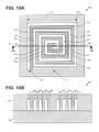
- FIG. 10A illustrates a top view of an embodiment of the invention's inductor.
- FIG. 10B illustrates a cross section view of an embodiment of the invention's inductor.
- FIG. 11 illustrates a cross section view of a layer of dielectric prior to fabrication of an inductor according to one embodiment of the invention.
- FIG. 12 illustrates the result of a metal deposition step during fabrication of an inductor according to one embodiment of the invention.
- FIG. 13 illustrates the patterned metal lines after patterning during fabrication of an inductor according to one embodiment of the invention.
- FIG. 14 illustrates the result of filling the gaps between the patterned metal lines with dielectric during fabrication of an inductor according to one embodiment of the invention.
- FIG. 15 illustrates the result of etching trenches between and adjacent to the patterned metal lines during fabrication of an inductor according to one embodiment of the invention.
- FIG. 16 illustrates the result of high permeability material deposition and chemical mechanical polish steps during fabrication of an inductor according to one embodiment of the invention.
- FIG. 17 illustrates a passivation layer deposited over an embodiment of the invention's inductor and shows the final structure according to one embodiment of the invention.
- FIG. 18 illustrates the result of a dielectric gap fill step showing dips that remain between the patterned metal lines during an alternative implementation of one embodiment of the invention.
- FIG. 19 illustrates the result of depositing high permeability material into the dips shown in FIG. 18 during fabrication of an inductor according to one embodiment of the invention.
- FIG. 20 illustrates a passivation layer deposited over one embodiment of the invention's inductor and shows the final structure according to an embodiment of the invention.
- the present invention is directed to method for fabrication of high inductance inductors and related structure.
- the following description contains specific information pertaining to different types of materials, layouts, dimensions, and implementations of the invention's inductor.
- One skilled in the art will recognize that the present invention may be practiced with material, layout, or dimensions different from those specifically discussed in the present application.
- some of the specific details of the invention are not discussed in order to not obscure the invention.
- the specific details not described in the present application are within the knowledge of a person of ordinary skills in the art.
- the magnetic dipoles of the material interact with the magnetic field created by the inductor. If the magnetic field of the inductor is reinforced by the magnetic moments, a larger number of flux lines are created, thus increasing the inductance.
- the ability of a material to reinforce the magnetic field of the inductor is determined by the permeability of the material. Permeability is the property of a material which describes the magnetization developed in that material when excited by a magnetic field.
- Equation 1 the permeability of dielectric 102 , which is situated within the magnetic field that will be created by metal turns 104 , 106 , 108 , and 110 of inductor 100 , was not included in Equation 1. This was because dielectric 102 was silicon dioxide or a low-k dielectric material in the example shown in FIG. 1 and the permeability of silicon dioxide or a low-k dielectric is approximately equal to 1.0. Therefore, Equation 1 would apply to materials, such as silicon dioxide, whose permeability is approximately equal to 1.0.
- L is the net effective inductance
- ⁇ is the relative permeability of the material placed within the magnetic field of the inductor
- n is the number of metal turns
- d is the “spiral diameter” which is a term used to refer to width 116 of inductor 100
- 0.38 is a coefficient which is derived empirically from the shape of the inductor.
- Equation 3 the net effective inductance can be increased by placing a material with a high permeability within the magnetic field of the inductor.
- materials that have very high permeability.
- a certain class of metals including iron and nickel, have relative permeability values in the thousands.
- Some alloys have even higher relative permeability values, some in the millions.
- nickel-iron alloys have a much higher permeability than iron alone.
- some magnetic oxides also have high values of permeability. These magnetic oxides are usually made of ferrites, i.e. crystalline minerals composed of iron oxide in combination with some other metal.
- a type of ferrite magnetic oxide having a spinel structure can be used as a high permeability material.
- a high permeability material such as one of those specifically mentioned above, is placed within the magnetic field of the inductor, ⁇ in Equation 3 will be high, resulting in a high inductance value for a given spiral diameter and a given number of metal turns.
- a high permeability material such as the ones mentioned above, is also referred to as a “permeability conversion material.”
- the present invention increases the inductance value of an inductor by fabricating structures between and adjacent to the metal turns of the inductor. These adjacent structures are fabricated using a high permeability material that replaces some of the dielectric material between the metal turns of the inductor. Thus, this high permeability material will be within the magnetic field of the inductor on a semiconductor die. For example, by fabricating the adjacent high permeability structures within the magnetic field of a square spiral inductor, the invention increases the inductance value of the square spiral inductor with a given spiral diameter and a given number of metal turns.
- trenches are etched into the area of dielectric between the metal turns of the inductor. These trenches may then be filled with a high permeability material. This filling step can be performed using sputtering or electroplating techniques known in the art.
- the metal turns of the inductor are patterned into the dielectric using the damascene process.
- the term “damascene” is derived from the ancient in-laid metal artistry originated in Damascus. According to the damascene process, trenches are cut into the dielectric and then filled with metal. Then, excess metal over the wafer surface is removed to form desired interconnect metal patterns within the trenches.
- FIG. 2A shows a top view of the invention's inductor 200 on an area of a semiconductor die.
- the inductor is configured as a square spiral inductor.
- the four metal turns of inductor 200 are referred to by numerals 204 , 206 , 208 , and 210 .
- metal turns 204 , 206 , 208 , and 210 are patterned within dielectric 202 using a damascene process.
- the areas of dielectric 202 which are flanked by metal turns 204 , 206 , 208 , and 210 are within the magnetic field that will be created by metal turns 204 , 206 , 208 , and 210 .
- Dielectric 202 can be silicon dioxide or a low-k dielectric.
- low-k dielectrics that can be used in the present embodiment are porous silica, fluorinated amorphous carbon, aromatic hydrocarbon, carbon-doped oxide, parylene, polyarylene ether, silsesquioxane, fluorinated silicon dioxide, and diamondlike carbon. All of these dielectrics have a dielectric constant below the widely used dielectrics silicon dioxide which has a dielectric constant of approximately 4.0.
- Metal turns 204 , 206 , 208 , and 210 can be aluminum, copper, or a copper-aluminum alloy.
- Metal turns 204 , 206 , 208 , and 210 are patterned on one metal layer.
- Metal turn 210 comprises connection terminal 212 .
- Connection terminal 212 is thus a part of inductor 200 while also functioning as a first connection terminal of inductor 200 .
- Connection terminal 214 is also a part of inductor 200 and functions as a second connection terminal of inductor 200 .
- connection terminal 214 is patterned on a different metal layer of the die than the rest of inductor 200 to allow connection terminal 214 to cross underneath metal turns 204 , 206 , 208 , and 210 of inductor 200 without shorting the metal turns together.
- An electrical connection between connection terminal 214 and metal turn 204 of inductor 200 is then provided, for example, by means of a via.
- Connection terminal 214 is shown in a different shade to show that it is situated on a different metal layer of the die than the remainder of the metal used to fabricate inductor 200 .
- the width of inductor 200 is referred to in FIG. 2A by numeral 216 .
- metal turns 204 , 206 , 208 , and 210 of inductor 200 are also referred to as a “conductor” patterned in a dielectric.
- High permeability material turns 220 , 222 , 224 , and 226 are situated between and are adjacent to metal turns 204 , 206 , 208 , and 210 of inductor 200 .
- High permeability material turns 220 , 222 , 224 , and 226 are shown in a different shade than metal turns 204 , 206 , 208 , and 210 .
- FIG. 2B shows a cross section of inductor 200 . Where the cross section is taken 20 is shown in FIG. 2A by the dashed line 2 B, also referred to by numeral 201 .
- FIG. 2B illustrates cross-section views 204 , 206 , 208 , and 210 corresponding to metal turns 204 , 206 , 208 , and 210 in FIG. 2 A.
- FIG. 2B illustrates cross-section views 220 , 222 , 224 , and 226 corresponding to high permeability material turns 220 , 222 , 224 , and 226 in FIG. 2 A.
- metal turns 204 , 206 , 208 , and 210 and only cross-section views of high permeability material turns 220 , 222 , 224 , and 226 are shown in FIG. 2B, these disjointed cross-section views will be referred to as metal turns 204 , 206 , 208 , and 210 and high permeability material turns 220 , 222 , 224 , and 226 , respectively, for simplicity.
- these metal turns and high permeability material turns of inductor 200 are patterned into the topmost metal layer of the semiconductor die. Although the topmost metal layer is used in the this embodiment, the invention could be implemented on any metal layer of the die.
- FIGS. 2A and 2B show inductor 200 after completion of this embodiment's process.
- FIGS. 3 through 9 illustrate the various steps of this embodiment's process by showing the cross sections of the resulting structures after each process step.
- FIG. 3 shows the first step of the invention's process in the present embodiment.
- the process begins with a layer of dielectric, referred to by numeral 202 .
- dielectric 202 can be silicon dioxide or a low-k dielectric.
- FIG. 4 shows the result of the next step in the invention's damascene process.
- Trenches 203 , 205 , 207 , and 209 are etched into dielectric 202 .
- trenches 203 , 205 , 207 , and 209 are patterned into dielectric 202 to form the square spiral shape of inductor 200 .
- FIG. 5 shows the result of the next step in the invention's process.
- Trenches 203 , 205 , 207 , and 209 have been filled with copper, in a manner known in the art, to form metal turns 204 , 206 , 208 , and 210 .
- Segments of dielectric 202 are situated between metal turns 204 , 206 , 208 , and 210 .
- CMP chemical mechanical polish
- the abrasive component is typically comprised of finely ground colloidal silica or alumina particles.
- the chemically reactive component is typically diluted acid and/or hydrogen peroxide, with the remainder of the slurry comprised of deionized water. After the CMP step, the surface of inductor 200 is substantially planarized.
- FIG. 6 shows the result of the next step in the invention's process.
- high permeability structures are fabricated between and adjacent to metal turns 204 , 206 , 208 , and 210 of inductor 200 .
- these structures form a continuous spiral structure.
- trenches 219 , 221 , 223 , and 225 have been etched, in a manner known in the art, between and adjacent to metal turns 204 , 206 , 208 , and 210 of inductor 200 .
- Width 231 of each of the trenches 219 , 221 , 223 , and 225 is chosen such that portions of dielectric 202 will be left on metal turns 204 , 206 , 208 , and 210 . These portions of dielectric 202 provide an insulation barrier between the copper in metal turns 204 , 206 , 208 , and 210 and the high permeability material that will be deposited into trenches 219 , 221 , 223 , and 225 in a subsequent step of the invention's process.
- trenches 219 , 221 , 223 , and 225 are shown as being the same depth as metal turns 204 , 206 , 208 , and 210 , trenches 219 , 221 , 223 , and 225 do not have to reach to the full depth of metal turns 204 , 206 , 208 , and 210 , and can have a different depth, for example, a depth equal to approximately one-half the depth (i.e. one-half the thickness) of metal turns 204 , 206 , 208 , and 210 .
- FIG. 7 shows the result of the next step in the invention's process.
- High permeability material 228 has been deposited over the area of the semiconductor die where inductor 200 is situated.
- the high permeability material fills trenches 219 , 221 , 223 , and 225 to form high permeability material turns 220 , 222 , 224 , and 226 .
- excess high permeability material is formed on top of inductor 200 during the high permeability material deposition step. This excess high permeability material will be removed in a subsequent step in the process.
- a first alternative is to deposit the high permeability material by sputtering.
- a second alternative is to deposit the high permeability material by electroplating. If sputtering is used as the deposition technique, a high permeability target is placed in a vacuum chamber along with the semiconductor die. The target is grounded and, as an example, a gas such as argon within the chamber is ionized to create positive ions of argon which are then attracted to the grounded high permeability target. The argon ions collide with the target material and the collision causes atoms and/or molecules of the high permeability target material to scatter from the target onto the die's surface.
- a seed layer of the high permeability material can first be deposited by sputtering before the electroplating step is performed.
- FIG. 8 shows the result of the next step in the invention's damascene process.
- Excess high permeability material 228 has been removed during a CMP step and the surface of the inductor is substantially flush with dielectric 202 .
- the type and ratio of abrasive and chemically reactive components in the CMP slurry can be determined, in a manner known in the art, to optimally remove the high permeability material.
- excess high permeability material 228 may be removed by etching in a manner known in the art.
- FIG. 9 shows the result of the next step in the invention's process.
- Passivation layer 218 has been deposited over the area of the semiconductor die where the inductor is situated. Passivation layer 218 prevents the copper in metal turns 204 , 206 , 208 , and 210 from diffusing onto the surface of the semiconductor die, which would result in long-term reliability problems. It is noted that passivation layer 218 was not shown in FIGS. 2A and 2B in order to not obscure the views of the invention's inductor 200 shown there. Passivation layer 218 can be silicon nitride.
- an anneal may be performed to electrically activate the high permeability material within trenches 219 , 221 , 223 , and 225 prior to the deposition of passivation layer 218 on the die.
- a typical anneal within a hydrogen atmosphere in a tube furnace will take place at a temperature of between 300 and 1000 degrees Centigrade.
- a subtractive etch process is used instead of the damascene process to fabricate the invention's inductor.
- the subtractive etch process begins with depositing a blanket layer of metal, such as aluminum, on a layer of dielectric. Thereafter, the metal layer is patterned and etched. During a “gap fill” process, the gaps between the patterned metal lines which remain after etching are filled with a dielectric.
- FIG. 10A shows a top view of the invention's inductor 300 on an area of a semiconductor die
- FIG. 10B illustrates a cross-section view, taken along dashed line 10 B, of the top view shown in FIG. 10 A.
- the inductor is configured as a square spiral inductor.
- the four metal turns of inductor 300 are referred to by numerals 304 , 306 , 308 , and 310 .
- Metal turns 304 , 306 , 308 , 310 , and dielectric 303 are fabricated using a subtractive etch process.
- dielectric 303 is situated on top of dielectric 302 and is also situated over and between metal turns 304 , 306 , 308 , and 310 .
- Metal turns 304 , 306 , 308 , and 310 are shown in the top view of the invention's inductor shown in FIG. 10A, although it is noted that metal turns 304 , 306 , 308 , and 310 would in fact be covered by dielectric 303 .
- the segments of dielectric 303 which are flanked by metal turns 304 , 306 , 308 , and 310 are within the magnetic field that will be created by metal turns 304 , 306 , 308 , and 310 .
- Dielectric 302 (shown in FIG. 10B) and dielectric 303 can be silicon dioxide or a low-k dielectric.
- examples of low-k dielectrics that can be used in this second embodiment of the invention are porous silica, fluorinated amorphous carbon, aromatic hydrocarbon, carbon-doped oxide, parylene, polyarylene ether, silsesquioxane, fluorinated silicon dioxide, and diamondlike carbon.
- Metal turns 304 , 306 , 308 , and 310 can be aluminum, copper, or a copper-aluminum alloy. In the present application, metal turns 304 , 306 , 308 , and 310 of inductor 300 are also referred to as a “conductor” patterned in a dielectric.
- Metal turns 304 , 306 , 308 , and 310 are patterned on one metal layer.
- Metal turn 310 comprises connection terminal 312 .
- Connection terminal 312 is thus a part of inductor 300 while also functioning as a first connection terminal of inductor 300 .
- Connection terminal 314 is also a part of inductor 300 and functions as a second connection terminal of inductor 300 .
- connection terminal 314 is patterned on a different metal layer of the die than the rest of inductor 300 to allow connection terminal 314 to cross underneath metal turns 304 , 306 , 308 , and 310 of inductor 300 without shorting the metal turns together.
- An electrical connection between connection terminal 314 and metal turn 304 of inductor 300 is then provided, for example, by means of a via.
- Connection terminal 314 is shown in a different shade to show that it is situated on a different metal layer of the die than the remainder of the metal used to fabricate inductor 300 .
- the width of inductor 300 is referred to in FIG. 10A by numeral 316 .
- High permeability material turns 320 , 322 , 324 , and 326 are situated between and are adjacent to metal turns 304 , 306 , 308 , and 310 of inductor 300 .
- High permeability material turns 320 , 322 , 324 , and 326 are shown in a different shade than metal turns 304 , 306 , 308 , and 310 .
- FIG. 10B shows a cross section of inductor 300 . Where the cross section is taken is shown in FIG. 10A by the cross section line 10 B, also referred to by numeral 301 .
- FIG. 10B illustrates cross-section views 304 , 306 , 308 , and 310 corresponding to metal turns 304 , 306 , 308 , and 310 in FIG. 10 A.
- FIG. 10B illustrates cross-section views 320 , 322 , 324 , and 326 corresponding to high permeability material turns 320 , 322 , 324 , and 326 in FIG. 10 A.
- metal turns 304 , 306 , 308 , and 310 Although only cross-section views of metal turns 304 , 306 , 308 , and 310 and only cross section views of high permeability material turns 320 , 322 , 324 , and 326 are shown in FIG. 10B, these disjointed cross-section views will be referred to as metal turns 304 , 306 , 308 , and 310 and high permeability material turns 320 , 322 , 324 , and 326 , respectively, for simplicity.
- the metal turns and high permeability material turns of inductor 300 are patterned in a metal layer of the semiconductor die other than the topmost metal layer, i.e. any metal layer below the topmost metal layer.
- a metal layer of the semiconductor die other than the topmost metal layer, i.e. any metal layer below the topmost metal layer.
- FIGS. 10A and 10B show inductor 300 after completion of the present embodiment's process.
- FIGS. 11 through 17 illustrate the various steps of this embodiment's process by showing the cross sections of the resulting structures after each process step.
- FIG. 11 shows the first step of the process in the present embodiment.
- the invention's process begins with a layer of dielectric, referred to by numeral 302 .
- dielectric 302 can be silicon dioxide or a low-k dielectric.
- FIG. 12 shows the result of the next step in the present embodiment's process.
- a blanket layer of metal, for example aluminum, referred to by numeral 309 has been deposited, in a manner known in the art, on dielectric 302 .
- FIG. 13 shows the result of the next step in the present embodiment of the invention.
- Metal turns 304 , 306 , 308 , and 310 have been patterned and etched out of the blanket layer of aluminum 309 to form a desired pattern.
- metal turns 304 , 306 , 308 , and 310 are patterned to form the square spiral shape of inductor 300 .
- FIG. 14 shows the result of the next step in the invention's process.
- a layer of dielectric referred to by numeral 303 , is deposited over dielectric 302 and fills the gaps between the aluminum metal turns 304 , 306 , 308 , and 310 which remain after the previous etch step.
- the top of dielectric 303 extends a distance 305 over metal turns 304 , 306 , 308 , and 310 .
- Distance 305 is chosen to provide adequate insulation between metal turns 304 , 306 , 308 , and 310 and another metal layer (not shown in any of the Figures) that will be situated over dielectric 303 .
- a CMP step is then performed on dielectric 303 and the surface of dielectric 303 is substantially planarized.
- FIG. 15 shows the result of the next step in the invention's process.
- high permeability structures between and adjacent to metal turns 304 , 306 , 308 , and 310 of inductor 300 are fabricated. In the present embodiment these structures form a continuous spiral.
- trenches 319 , 321 , 323 , and 325 are first etched into the potions of dielectric 303 between and adjacent to metal turns 304 , 306 , 308 , and 310 of inductor 300 .
- trenches 319 , 321 , 323 , and 325 are patterned into dielectric 303 as a square spiral shape. Although trenches 319 , 321 , 323 , and 325 are shown as not extending to the full depth of metal turns 304 , 306 , 308 , and 310 , they could extend to a different depth, for example, to the same depth as metal turns 304 , 306 , 308 , and 310 .
- FIG. 16 shows the result of the next steps in the invention's process.
- a high permeability material has been deposited over the area of the semiconductor die where inductor 300 is situated.
- the high permeability material fills trenches 319 , 321 , 323 , and 325 to form high permeability material turns 320 , 322 , 324 , and 326 .
- Excess high permeability material (not shown in FIG. 16) is formed on top of inductor 300 during the high permeability material deposition step. This excess high permeability material is removed by a CMP or etch step as described above in relation to the first embodiment of the invention.
- the deposition of high permeability material can be performed using sputtering or other deposition techniques, including electroplating.
- FIG. 17 shows the result of the next step in the present embodiment's process.
- Passivation layer 318 has been deposited over the area of the semiconductor die where inductor 300 is situated. It is noted that passivation layer 318 was not shown in FIGS. 10A and 10B in order to not obscure the views of the invention's inductor 300 shown there.
- Passivation layer 318 can be silicon nitride.
- An optional anneal may be performed to electrically activate the high permeability material within trenches 319 , 321 , 323 , and 325 prior to the deposition of passivation layer 318 on the die. As stated above, a typical anneal within a hydrogen or nitrogen atmosphere in a tube furnace will take place at a temperature of between 300 and 1000 degrees Centigrade.
- FIGS. 18 through 20 illustrate the remaining steps of this implementation of the present embodiment.
- FIG. 18 shows the result of the next step.
- a layer of dielectric referred to by numeral 303 .
- metal turns 304 , 306 , 308 , and 310 are situated on the topmost metal layer of the semiconductor die. Therefore, dielectric 303 can be a thinner layer because there will not be another metal layer above dielectric 303 and less insulation is required.
- dips 329 , 331 , 333 , and 335 form in dielectric 303 between metal turns 304 , 306 , 308 , and 310 .
- FIG. 19 shows the result of the next step of the process.
- High permeability material 328 has been deposited over the area of the semiconductor die where the invention's inductor is situated.
- High permeability material 328 fills dips 329 , 331 , 333 , and 335 to form high permeability material segments 330 , 332 , 334 , and 336 .
- FIG. 20 shows the result of the subsequent steps. Excess high permeability material 328 that was formed on top of the invention's inductor during the high permeability material deposition step, along with excess dielectric 303 , is removed during a CMP or etch step. Passivation layer 318 has been deposited on the surface of the semiconductor die and covers the inductor.
- an optional anneal may be performed to electrically activate the high permeability material within dips 329 , 331 , 333 , and 335 prior to the deposition of passivation layer 318 on the die.
- a typical anneal within a hydrogen or nitrogen atmosphere in a tube furnace will take place at a temperature of between 300 and 1000 degrees Centigrade.
- high permeability material is deposited between and adjacent to the metal turns of the inductor and will be within the magnetic field of the inductor.
- the presence of this high permeability material within the magnetic field of the inductor's metal turns results in a higher inductance, as can be seen from Equation 3.
- the invention allows device engineers to increase the inductance of an on-chip inductor by depositing a high permeability material within the magnetic field of the inductor rather than by increasing the size of the on-chip inductor, which would require a larger area of the chip to be set aside for inductors. If very high permeability material such as a nickel-iron alloy is used, the deposition of the high permeability material between the metal turns of the inductor will result in a significant increase in the inductance.
- the invention's inductor will enable device engineers to include significantly more of the invention's inductors on a single chip, yielding significant advantages in circuit design and resulting in greater integration of passive components on a single chip.
Abstract
Description
Claims (20)
Priority Applications (3)
| Application Number | Priority Date | Filing Date | Title |
|---|---|---|---|
| US09/649,442 US6417755B1 (en) | 2000-08-25 | 2000-08-25 | Method for fabrication of high inductance inductors and related structure |
| PCT/US2001/026449 WO2002019351A1 (en) | 2000-08-25 | 2001-08-24 | Method for fabrication of high inductance inductors and related structure |
| AU2001286713A AU2001286713A1 (en) | 2000-08-25 | 2001-08-24 | Method for fabrication of high inductance inductors and related structure |
Applications Claiming Priority (1)
| Application Number | Priority Date | Filing Date | Title |
|---|---|---|---|
| US09/649,442 US6417755B1 (en) | 2000-08-25 | 2000-08-25 | Method for fabrication of high inductance inductors and related structure |
Publications (1)
| Publication Number | Publication Date |
|---|---|
| US6417755B1 true US6417755B1 (en) | 2002-07-09 |
Family
ID=24604802
Family Applications (1)
| Application Number | Title | Priority Date | Filing Date |
|---|---|---|---|
| US09/649,442 Expired - Lifetime US6417755B1 (en) | 2000-08-25 | 2000-08-25 | Method for fabrication of high inductance inductors and related structure |
Country Status (3)
| Country | Link |
|---|---|
| US (1) | US6417755B1 (en) |
| AU (1) | AU2001286713A1 (en) |
| WO (1) | WO2002019351A1 (en) |
Cited By (19)
| Publication number | Priority date | Publication date | Assignee | Title |
|---|---|---|---|---|
| US6459352B1 (en) * | 2001-02-08 | 2002-10-01 | Skyworks Solutions, Inc. | On-chip transformers |
| US20030048167A1 (en) * | 2001-08-29 | 2003-03-13 | Matsushita Electric Industrial Co., Ltd. | Magnetic device, method for manufacturing the same, and power supply module equipped with the same |
| US6534406B1 (en) * | 2000-09-22 | 2003-03-18 | Newport Fab, Llc | Method for increasing inductance of on-chip inductors and related structure |
| US20030066184A1 (en) * | 2001-10-10 | 2003-04-10 | Pascal Gardes | Inductance and its manufacturing method |
| US6714112B2 (en) * | 2002-05-10 | 2004-03-30 | Chartered Semiconductor Manufacturing Limited | Silicon-based inductor with varying metal-to-metal conductor spacing |
| KR100461536B1 (en) * | 2002-11-14 | 2004-12-16 | 한국전자통신연구원 | Inductor increased with quality factor and Method of arranging uint inductor increasing the same |
| US20050122198A1 (en) * | 2003-12-05 | 2005-06-09 | Yaping Zhou | Inductive device including bond wires |
| CN100370598C (en) * | 2004-01-22 | 2008-02-20 | 国际商业机器公司 | Method of manufacturing high performance copper inductors |
| US20080079115A1 (en) * | 2006-09-29 | 2008-04-03 | Freescale Semiconductor, Inc. | Electronic device including an inductor and a process of forming the same |
| US20100225435A1 (en) * | 2009-03-04 | 2010-09-09 | Qualcomm Incorporated | Magnetic Film Enhanced Inductor |
| US7875955B1 (en) | 2006-03-09 | 2011-01-25 | National Semiconductor Corporation | On-chip power inductor |
| JP2013504891A (en) * | 2009-09-16 | 2013-02-07 | マラディン テクノロジーズ リミテッド | Micro-coil device and manufacturing method thereof |
| US20150357112A1 (en) * | 2005-06-30 | 2015-12-10 | L. Pierre de Rochemont | Power Management Module and Method of Manufacture |
| US9590514B1 (en) | 2013-03-15 | 2017-03-07 | The Board Of Trustees Of The University Of Alabama, For And On Behalf Of The University Of Alabama | Carbon nanotube-based integrated power converters |
| US9793039B1 (en) * | 2011-05-04 | 2017-10-17 | The Board Of Trustees Of The University Of Alabama | Carbon nanotube-based integrated power inductor for on-chip switching power converters |
| US10424431B2 (en) | 2015-09-15 | 2019-09-24 | Xytech Electronic Technology (Shanghai) Co., Ltd. | Coil, inductor device and method for manufacturing the coil |
| US10685776B1 (en) * | 2016-04-01 | 2020-06-16 | The Board Of Trustees Of The University Of Alabama | Integrated magnetic inductors |
| US20210104345A1 (en) * | 2019-10-08 | 2021-04-08 | Murata Manufacturing Co., Ltd. | Inductor component and method for manufacturing inductor component |
| US11227716B2 (en) * | 2017-12-11 | 2022-01-18 | Samsung Electro-Mechanics Co., Ltd. | Inductor |
Citations (7)
| Publication number | Priority date | Publication date | Assignee | Title |
|---|---|---|---|---|
| US5372967A (en) * | 1992-01-27 | 1994-12-13 | Motorola, Inc. | Method for fabricating a vertical trench inductor |
| US5884990A (en) * | 1996-08-23 | 1999-03-23 | International Business Machines Corporation | Integrated circuit inductor |
| US6008102A (en) * | 1998-04-09 | 1999-12-28 | Motorola, Inc. | Method of forming a three-dimensional integrated inductor |
| US6057202A (en) * | 1998-01-16 | 2000-05-02 | Windbond Electronics Corp. | Method for manufacturing an inductor with resonant frequency and Q value increased in semiconductor process |
| US6060976A (en) | 1996-01-30 | 2000-05-09 | Alps Electric Co., Ltd. | Plane transformer |
| US6084500A (en) | 1997-03-28 | 2000-07-04 | Matsushita Electric Industrial Co., Ltd. | Chip inductor and method for manufacturing the same |
| US6131041A (en) | 1996-10-11 | 2000-10-10 | Matsushita Electric Industrial Co., Ltd. | Wireless terminal equipment including electric component having conductor film formed on insulative base |
-
2000
- 2000-08-25 US US09/649,442 patent/US6417755B1/en not_active Expired - Lifetime
-
2001
- 2001-08-24 AU AU2001286713A patent/AU2001286713A1/en not_active Abandoned
- 2001-08-24 WO PCT/US2001/026449 patent/WO2002019351A1/en active Application Filing
Patent Citations (9)
| Publication number | Priority date | Publication date | Assignee | Title |
|---|---|---|---|---|
| US5372967A (en) * | 1992-01-27 | 1994-12-13 | Motorola, Inc. | Method for fabricating a vertical trench inductor |
| US6060976A (en) | 1996-01-30 | 2000-05-09 | Alps Electric Co., Ltd. | Plane transformer |
| US5884990A (en) * | 1996-08-23 | 1999-03-23 | International Business Machines Corporation | Integrated circuit inductor |
| US6054329A (en) * | 1996-08-23 | 2000-04-25 | International Business Machines Corporation | Method of forming an integrated circuit spiral inductor with ferromagnetic liner |
| US6114937A (en) | 1996-08-23 | 2000-09-05 | International Business Machines Corporation | Integrated circuit spiral inductor |
| US6131041A (en) | 1996-10-11 | 2000-10-10 | Matsushita Electric Industrial Co., Ltd. | Wireless terminal equipment including electric component having conductor film formed on insulative base |
| US6084500A (en) | 1997-03-28 | 2000-07-04 | Matsushita Electric Industrial Co., Ltd. | Chip inductor and method for manufacturing the same |
| US6057202A (en) * | 1998-01-16 | 2000-05-02 | Windbond Electronics Corp. | Method for manufacturing an inductor with resonant frequency and Q value increased in semiconductor process |
| US6008102A (en) * | 1998-04-09 | 1999-12-28 | Motorola, Inc. | Method of forming a three-dimensional integrated inductor |
Cited By (32)
| Publication number | Priority date | Publication date | Assignee | Title |
|---|---|---|---|---|
| US6534406B1 (en) * | 2000-09-22 | 2003-03-18 | Newport Fab, Llc | Method for increasing inductance of on-chip inductors and related structure |
| US6459352B1 (en) * | 2001-02-08 | 2002-10-01 | Skyworks Solutions, Inc. | On-chip transformers |
| US20030048167A1 (en) * | 2001-08-29 | 2003-03-13 | Matsushita Electric Industrial Co., Ltd. | Magnetic device, method for manufacturing the same, and power supply module equipped with the same |
| US6768409B2 (en) * | 2001-08-29 | 2004-07-27 | Matsushita Electric Industrial Co., Ltd. | Magnetic device, method for manufacturing the same, and power supply module equipped with the same |
| US7404249B2 (en) * | 2001-10-10 | 2008-07-29 | Stmicroelectronics S.A. | Method of manufacturing an inductance |
| US20030066184A1 (en) * | 2001-10-10 | 2003-04-10 | Pascal Gardes | Inductance and its manufacturing method |
| US6714112B2 (en) * | 2002-05-10 | 2004-03-30 | Chartered Semiconductor Manufacturing Limited | Silicon-based inductor with varying metal-to-metal conductor spacing |
| KR100461536B1 (en) * | 2002-11-14 | 2004-12-16 | 한국전자통신연구원 | Inductor increased with quality factor and Method of arranging uint inductor increasing the same |
| US20050122198A1 (en) * | 2003-12-05 | 2005-06-09 | Yaping Zhou | Inductive device including bond wires |
| US6998952B2 (en) | 2003-12-05 | 2006-02-14 | Freescale Semiconductor, Inc. | Inductive device including bond wires |
| CN100370598C (en) * | 2004-01-22 | 2008-02-20 | 国际商业机器公司 | Method of manufacturing high performance copper inductors |
| US20150357112A1 (en) * | 2005-06-30 | 2015-12-10 | L. Pierre de Rochemont | Power Management Module and Method of Manufacture |
| US10475568B2 (en) * | 2005-06-30 | 2019-11-12 | L. Pierre De Rochemont | Power management module and method of manufacture |
| US7875955B1 (en) | 2006-03-09 | 2011-01-25 | National Semiconductor Corporation | On-chip power inductor |
| US7524731B2 (en) | 2006-09-29 | 2009-04-28 | Freescale Semiconductor, Inc. | Process of forming an electronic device including an inductor |
| US20090152676A1 (en) * | 2006-09-29 | 2009-06-18 | Freescale Semiconductor, Inc. | Electronic device including an inductor |
| US7619297B2 (en) | 2006-09-29 | 2009-11-17 | Freescale Semiconductor, Inc. | Electronic device including an inductor |
| US20080079115A1 (en) * | 2006-09-29 | 2008-04-03 | Freescale Semiconductor, Inc. | Electronic device including an inductor and a process of forming the same |
| CN102341870B (en) * | 2009-03-04 | 2015-07-15 | 高通股份有限公司 | Magnetic Film Enhanced Inductor |
| US20100225435A1 (en) * | 2009-03-04 | 2010-09-09 | Qualcomm Incorporated | Magnetic Film Enhanced Inductor |
| JP2012519395A (en) * | 2009-03-04 | 2012-08-23 | クアルコム,インコーポレイテッド | Magnetic film reinforced inductor |
| KR101304387B1 (en) * | 2009-03-04 | 2013-09-11 | 퀄컴 인코포레이티드 | Magnetic film enhanced inductor |
| CN102341870A (en) * | 2009-03-04 | 2012-02-01 | 高通股份有限公司 | Magnetic Film Enhanced Inductor |
| US9190201B2 (en) | 2009-03-04 | 2015-11-17 | Qualcomm Incorporated | Magnetic film enhanced inductor |
| WO2010102132A1 (en) * | 2009-03-04 | 2010-09-10 | Qualcomm Incorporated | Magnetic film enhanced inductor |
| JP2013504891A (en) * | 2009-09-16 | 2013-02-07 | マラディン テクノロジーズ リミテッド | Micro-coil device and manufacturing method thereof |
| US9793039B1 (en) * | 2011-05-04 | 2017-10-17 | The Board Of Trustees Of The University Of Alabama | Carbon nanotube-based integrated power inductor for on-chip switching power converters |
| US9590514B1 (en) | 2013-03-15 | 2017-03-07 | The Board Of Trustees Of The University Of Alabama, For And On Behalf Of The University Of Alabama | Carbon nanotube-based integrated power converters |
| US10424431B2 (en) | 2015-09-15 | 2019-09-24 | Xytech Electronic Technology (Shanghai) Co., Ltd. | Coil, inductor device and method for manufacturing the coil |
| US10685776B1 (en) * | 2016-04-01 | 2020-06-16 | The Board Of Trustees Of The University Of Alabama | Integrated magnetic inductors |
| US11227716B2 (en) * | 2017-12-11 | 2022-01-18 | Samsung Electro-Mechanics Co., Ltd. | Inductor |
| US20210104345A1 (en) * | 2019-10-08 | 2021-04-08 | Murata Manufacturing Co., Ltd. | Inductor component and method for manufacturing inductor component |
Also Published As
| Publication number | Publication date |
|---|---|
| AU2001286713A1 (en) | 2002-03-13 |
| WO2002019351A1 (en) | 2002-03-07 |
Similar Documents
| Publication | Publication Date | Title |
|---|---|---|
| US6417755B1 (en) | Method for fabrication of high inductance inductors and related structure | |
| US7436281B2 (en) | Method to improve inductance with a high-permeability slotted plate core in an integrated circuit | |
| US6163234A (en) | Micromagnetic device for data transmission applications and method of manufacture therefor | |
| JP4948756B2 (en) | Inductor formed in integrated circuit and method of manufacturing the same | |
| KR100801455B1 (en) | Method of fabricating flux concentrating layer for use with magnetoresistive random access memories | |
| KR100939648B1 (en) | A multi-layer inductor formed in a semiconductor substrate | |
| EP1831918B1 (en) | Fabrication of a ferromagnetic inductor core and capacitor electrode in a single photo mask step | |
| US6903644B2 (en) | Inductor device having improved quality factor | |
| US6459352B1 (en) | On-chip transformers | |
| US20030170989A1 (en) | Semiconductor inductor and methods for making the same | |
| TWI412119B (en) | Semiconductor device | |
| US6396122B1 (en) | Method for fabricating on-chip inductors and related structure | |
| JP4584533B2 (en) | Thin film multilayer high Q transformer formed in a semiconductor substrate | |
| US6909188B2 (en) | Semiconductor device and manufacturing method thereof | |
| US8531002B2 (en) | Apparatus and method for wafer level fabrication of high value inductors on semiconductor integrated circuits | |
| US6191495B1 (en) | Micromagnetic device having an anisotropic ferromagnetic core and method of manufacture therefor | |
| US6309922B1 (en) | Method for fabrication of on-chip inductors and related structure | |
| US6319616B1 (en) | Scaled interconnect anodization for high frequency applications | |
| US7247565B2 (en) | Methods for fabricating a copper interconnect | |
| JP5090688B2 (en) | Semiconductor device | |
| US6534406B1 (en) | Method for increasing inductance of on-chip inductors and related structure | |
| US7078239B2 (en) | Integrated circuit structure formed by damascene process |
Legal Events
| Date | Code | Title | Description |
|---|---|---|---|
| AS | Assignment |
Owner name: CONEXANT SYSTEMS, INC., CALIFORNIA Free format text: ASSIGNMENT OF ASSIGNORS INTEREST;ASSIGNORS:LIU, Q.Z.;HOWARD, DAVID;REEL/FRAME:011042/0283 Effective date: 20000823 |
|
| AS | Assignment |
Owner name: NEWPORT FAB, LLC, CALIFORNIA Free format text: ASSIGNMENT OF ASSIGNORS INTEREST;ASSIGNOR:CONEXANT SYSTEMS, INC.;REEL/FRAME:012754/0852 Effective date: 20020312 |
|
| STCF | Information on status: patent grant |
Free format text: PATENTED CASE |
|
| AS | Assignment |
Owner name: NEWPORT FAB, LLC, CALIFORNIA Free format text: ASSIGNMENT OF ASSIGNORS INTEREST;ASSIGNOR:CONEXANT SYSTEMS, INC.;REEL/FRAME:013280/0690 Effective date: 20020312 |
|
| FPAY | Fee payment |
Year of fee payment: 4 |
|
| AS | Assignment |
Owner name: WACHOVIA CAPITAL FINANCE CORPORATION (WESTERN), CA Free format text: SECURITY AGREEMENT;ASSIGNOR:NEWPORT FAB, LLC;REEL/FRAME:017223/0083 Effective date: 20060106 |
|
| AS | Assignment |
Owner name: WACHOVIA CAPITAL FINANCE CORPORATION (WESTERN), CA Free format text: SECURITY AGREEMENT;ASSIGNOR:NEWPORT FAB, LLC;REEL/FRAME:017586/0081 Effective date: 20060106 |
|
| FPAY | Fee payment |
Year of fee payment: 8 |
|
| FPAY | Fee payment |
Year of fee payment: 12 |
|
| FEPP | Fee payment procedure |
Free format text: PAYER NUMBER DE-ASSIGNED (ORIGINAL EVENT CODE: RMPN); ENTITY STATUS OF PATENT OWNER: LARGE ENTITY Free format text: PAYOR NUMBER ASSIGNED (ORIGINAL EVENT CODE: ASPN); ENTITY STATUS OF PATENT OWNER: LARGE ENTITY |
|
| AS | Assignment |
Owner name: NEWPORT FAB, LLC DBA JAZZ SEMICONDUCTOR OPERATING COMPANY, CALIFORNIA Free format text: RELEASE BY SECURED PARTY;ASSIGNOR:WELLS FARGO CAPITAL FINANCE, LLC, AS SUCCESSOR BY MERGER TO WACHOVIA CAPITAL FINANCE CORPORATION (WESTERN);REEL/FRAME:065284/0123 Effective date: 20230929 |