US6407381B1 - Wafer scale image sensor package - Google Patents
Wafer scale image sensor package Download PDFInfo
- Publication number
- US6407381B1 US6407381B1 US09/610,314 US61031400A US6407381B1 US 6407381 B1 US6407381 B1 US 6407381B1 US 61031400 A US61031400 A US 61031400A US 6407381 B1 US6407381 B1 US 6407381B1
- Authority
- US
- United States
- Prior art keywords
- window
- image sensor
- active area
- package
- window support
- Prior art date
- Legal status (The legal status is an assumption and is not a legal conclusion. Google has not performed a legal analysis and makes no representation as to the accuracy of the status listed.)
- Expired - Lifetime
Links
- 239000000758 substrate Substances 0.000 claims description 58
- 230000005855 radiation Effects 0.000 claims description 37
- 239000004593 Epoxy Substances 0.000 claims description 7
- 241000763859 Dyckia brevifolia Species 0.000 description 26
- 238000000034 method Methods 0.000 description 22
- 239000000463 material Substances 0.000 description 20
- 238000004519 manufacturing process Methods 0.000 description 19
- 230000000712 assembly Effects 0.000 description 17
- 238000000429 assembly Methods 0.000 description 17
- 230000005670 electromagnetic radiation Effects 0.000 description 15
- 230000006378 damage Effects 0.000 description 13
- XUIMIQQOPSSXEZ-UHFFFAOYSA-N Silicon Chemical compound [Si] XUIMIQQOPSSXEZ-UHFFFAOYSA-N 0.000 description 9
- 229910052710 silicon Inorganic materials 0.000 description 9
- 239000010703 silicon Substances 0.000 description 9
- 238000009833 condensation Methods 0.000 description 8
- 230000005494 condensation Effects 0.000 description 8
- 230000037361 pathway Effects 0.000 description 8
- 230000015572 biosynthetic process Effects 0.000 description 7
- 238000011109 contamination Methods 0.000 description 7
- 238000005520 cutting process Methods 0.000 description 7
- 239000008393 encapsulating agent Substances 0.000 description 7
- 238000004806 packaging method and process Methods 0.000 description 7
- 230000035945 sensitivity Effects 0.000 description 7
- 239000000919 ceramic Substances 0.000 description 5
- 239000007788 liquid Substances 0.000 description 5
- 239000000428 dust Substances 0.000 description 4
- 238000005538 encapsulation Methods 0.000 description 4
- 238000000465 moulding Methods 0.000 description 4
- 239000012777 electrically insulating material Substances 0.000 description 3
- 239000005022 packaging material Substances 0.000 description 3
- 238000003825 pressing Methods 0.000 description 3
- 238000006748 scratching Methods 0.000 description 3
- 230000002393 scratching effect Effects 0.000 description 3
- 229910000679 solder Inorganic materials 0.000 description 3
- 239000000853 adhesive Substances 0.000 description 2
- 230000001070 adhesive effect Effects 0.000 description 2
- 239000005388 borosilicate glass Substances 0.000 description 2
- 230000002950 deficient Effects 0.000 description 2
- 239000002184 metal Substances 0.000 description 2
- 238000012986 modification Methods 0.000 description 2
- 230000004048 modification Effects 0.000 description 2
- 229920001296 polysiloxane Polymers 0.000 description 2
- 238000007650 screen-printing Methods 0.000 description 2
- 230000003247 decreasing effect Effects 0.000 description 1
- 238000003698 laser cutting Methods 0.000 description 1
- 238000001020 plasma etching Methods 0.000 description 1
- 238000004528 spin coating Methods 0.000 description 1
- 239000000126 substance Substances 0.000 description 1
- 238000002834 transmittance Methods 0.000 description 1
Images


Classifications
-
- H—ELECTRICITY
- H01—ELECTRIC ELEMENTS
- H01L—SEMICONDUCTOR DEVICES NOT COVERED BY CLASS H10
- H01L31/00—Semiconductor devices sensitive to infrared radiation, light, electromagnetic radiation of shorter wavelength or corpuscular radiation and specially adapted either for the conversion of the energy of such radiation into electrical energy or for the control of electrical energy by such radiation; Processes or apparatus specially adapted for the manufacture or treatment thereof or of parts thereof; Details thereof
- H01L31/02—Details
- H01L31/0203—Containers; Encapsulations, e.g. encapsulation of photodiodes
-
- H—ELECTRICITY
- H01—ELECTRIC ELEMENTS
- H01L—SEMICONDUCTOR DEVICES NOT COVERED BY CLASS H10
- H01L24/00—Arrangements for connecting or disconnecting semiconductor or solid-state bodies; Methods or apparatus related thereto
- H01L24/93—Batch processes
- H01L24/94—Batch processes at wafer-level, i.e. with connecting carried out on a wafer comprising a plurality of undiced individual devices
-
- H—ELECTRICITY
- H01—ELECTRIC ELEMENTS
- H01L—SEMICONDUCTOR DEVICES NOT COVERED BY CLASS H10
- H01L27/00—Devices consisting of a plurality of semiconductor or other solid-state components formed in or on a common substrate
- H01L27/14—Devices consisting of a plurality of semiconductor or other solid-state components formed in or on a common substrate including semiconductor components sensitive to infrared radiation, light, electromagnetic radiation of shorter wavelength or corpuscular radiation and specially adapted either for the conversion of the energy of such radiation into electrical energy or for the control of electrical energy by such radiation
- H01L27/144—Devices controlled by radiation
- H01L27/146—Imager structures
- H01L27/14601—Structural or functional details thereof
- H01L27/14618—Containers
-
- H—ELECTRICITY
- H01—ELECTRIC ELEMENTS
- H01L—SEMICONDUCTOR DEVICES NOT COVERED BY CLASS H10
- H01L2224/00—Indexing scheme for arrangements for connecting or disconnecting semiconductor or solid-state bodies and methods related thereto as covered by H01L24/00
- H01L2224/01—Means for bonding being attached to, or being formed on, the surface to be connected, e.g. chip-to-package, die-attach, "first-level" interconnects; Manufacturing methods related thereto
- H01L2224/26—Layer connectors, e.g. plate connectors, solder or adhesive layers; Manufacturing methods related thereto
- H01L2224/31—Structure, shape, material or disposition of the layer connectors after the connecting process
- H01L2224/32—Structure, shape, material or disposition of the layer connectors after the connecting process of an individual layer connector
- H01L2224/321—Disposition
- H01L2224/32151—Disposition the layer connector connecting between a semiconductor or solid-state body and an item not being a semiconductor or solid-state body, e.g. chip-to-substrate, chip-to-passive
- H01L2224/32221—Disposition the layer connector connecting between a semiconductor or solid-state body and an item not being a semiconductor or solid-state body, e.g. chip-to-substrate, chip-to-passive the body and the item being stacked
- H01L2224/32225—Disposition the layer connector connecting between a semiconductor or solid-state body and an item not being a semiconductor or solid-state body, e.g. chip-to-substrate, chip-to-passive the body and the item being stacked the item being non-metallic, e.g. insulating substrate with or without metallisation
-
- H—ELECTRICITY
- H01—ELECTRIC ELEMENTS
- H01L—SEMICONDUCTOR DEVICES NOT COVERED BY CLASS H10
- H01L2224/00—Indexing scheme for arrangements for connecting or disconnecting semiconductor or solid-state bodies and methods related thereto as covered by H01L24/00
- H01L2224/01—Means for bonding being attached to, or being formed on, the surface to be connected, e.g. chip-to-package, die-attach, "first-level" interconnects; Manufacturing methods related thereto
- H01L2224/26—Layer connectors, e.g. plate connectors, solder or adhesive layers; Manufacturing methods related thereto
- H01L2224/31—Structure, shape, material or disposition of the layer connectors after the connecting process
- H01L2224/32—Structure, shape, material or disposition of the layer connectors after the connecting process of an individual layer connector
- H01L2224/321—Disposition
- H01L2224/32151—Disposition the layer connector connecting between a semiconductor or solid-state body and an item not being a semiconductor or solid-state body, e.g. chip-to-substrate, chip-to-passive
- H01L2224/32221—Disposition the layer connector connecting between a semiconductor or solid-state body and an item not being a semiconductor or solid-state body, e.g. chip-to-substrate, chip-to-passive the body and the item being stacked
- H01L2224/32245—Disposition the layer connector connecting between a semiconductor or solid-state body and an item not being a semiconductor or solid-state body, e.g. chip-to-substrate, chip-to-passive the body and the item being stacked the item being metallic
-
- H—ELECTRICITY
- H01—ELECTRIC ELEMENTS
- H01L—SEMICONDUCTOR DEVICES NOT COVERED BY CLASS H10
- H01L2224/00—Indexing scheme for arrangements for connecting or disconnecting semiconductor or solid-state bodies and methods related thereto as covered by H01L24/00
- H01L2224/01—Means for bonding being attached to, or being formed on, the surface to be connected, e.g. chip-to-package, die-attach, "first-level" interconnects; Manufacturing methods related thereto
- H01L2224/42—Wire connectors; Manufacturing methods related thereto
- H01L2224/47—Structure, shape, material or disposition of the wire connectors after the connecting process
- H01L2224/48—Structure, shape, material or disposition of the wire connectors after the connecting process of an individual wire connector
- H01L2224/4805—Shape
- H01L2224/4809—Loop shape
- H01L2224/48091—Arched
-
- H—ELECTRICITY
- H01—ELECTRIC ELEMENTS
- H01L—SEMICONDUCTOR DEVICES NOT COVERED BY CLASS H10
- H01L2224/00—Indexing scheme for arrangements for connecting or disconnecting semiconductor or solid-state bodies and methods related thereto as covered by H01L24/00
- H01L2224/01—Means for bonding being attached to, or being formed on, the surface to be connected, e.g. chip-to-package, die-attach, "first-level" interconnects; Manufacturing methods related thereto
- H01L2224/42—Wire connectors; Manufacturing methods related thereto
- H01L2224/47—Structure, shape, material or disposition of the wire connectors after the connecting process
- H01L2224/48—Structure, shape, material or disposition of the wire connectors after the connecting process of an individual wire connector
- H01L2224/481—Disposition
- H01L2224/48151—Connecting between a semiconductor or solid-state body and an item not being a semiconductor or solid-state body, e.g. chip-to-substrate, chip-to-passive
- H01L2224/48221—Connecting between a semiconductor or solid-state body and an item not being a semiconductor or solid-state body, e.g. chip-to-substrate, chip-to-passive the body and the item being stacked
- H01L2224/48225—Connecting between a semiconductor or solid-state body and an item not being a semiconductor or solid-state body, e.g. chip-to-substrate, chip-to-passive the body and the item being stacked the item being non-metallic, e.g. insulating substrate with or without metallisation
- H01L2224/48227—Connecting between a semiconductor or solid-state body and an item not being a semiconductor or solid-state body, e.g. chip-to-substrate, chip-to-passive the body and the item being stacked the item being non-metallic, e.g. insulating substrate with or without metallisation connecting the wire to a bond pad of the item
-
- H—ELECTRICITY
- H01—ELECTRIC ELEMENTS
- H01L—SEMICONDUCTOR DEVICES NOT COVERED BY CLASS H10
- H01L2224/00—Indexing scheme for arrangements for connecting or disconnecting semiconductor or solid-state bodies and methods related thereto as covered by H01L24/00
- H01L2224/01—Means for bonding being attached to, or being formed on, the surface to be connected, e.g. chip-to-package, die-attach, "first-level" interconnects; Manufacturing methods related thereto
- H01L2224/42—Wire connectors; Manufacturing methods related thereto
- H01L2224/47—Structure, shape, material or disposition of the wire connectors after the connecting process
- H01L2224/48—Structure, shape, material or disposition of the wire connectors after the connecting process of an individual wire connector
- H01L2224/481—Disposition
- H01L2224/48151—Connecting between a semiconductor or solid-state body and an item not being a semiconductor or solid-state body, e.g. chip-to-substrate, chip-to-passive
- H01L2224/48221—Connecting between a semiconductor or solid-state body and an item not being a semiconductor or solid-state body, e.g. chip-to-substrate, chip-to-passive the body and the item being stacked
- H01L2224/48245—Connecting between a semiconductor or solid-state body and an item not being a semiconductor or solid-state body, e.g. chip-to-substrate, chip-to-passive the body and the item being stacked the item being metallic
- H01L2224/48247—Connecting between a semiconductor or solid-state body and an item not being a semiconductor or solid-state body, e.g. chip-to-substrate, chip-to-passive the body and the item being stacked the item being metallic connecting the wire to a bond pad of the item
-
- H—ELECTRICITY
- H01—ELECTRIC ELEMENTS
- H01L—SEMICONDUCTOR DEVICES NOT COVERED BY CLASS H10
- H01L2224/00—Indexing scheme for arrangements for connecting or disconnecting semiconductor or solid-state bodies and methods related thereto as covered by H01L24/00
- H01L2224/73—Means for bonding being of different types provided for in two or more of groups H01L2224/10, H01L2224/18, H01L2224/26, H01L2224/34, H01L2224/42, H01L2224/50, H01L2224/63, H01L2224/71
- H01L2224/732—Location after the connecting process
- H01L2224/73251—Location after the connecting process on different surfaces
- H01L2224/73265—Layer and wire connectors
-
- H—ELECTRICITY
- H01—ELECTRIC ELEMENTS
- H01L—SEMICONDUCTOR DEVICES NOT COVERED BY CLASS H10
- H01L23/00—Details of semiconductor or other solid state devices
- H01L23/28—Encapsulations, e.g. encapsulating layers, coatings, e.g. for protection
- H01L23/31—Encapsulations, e.g. encapsulating layers, coatings, e.g. for protection characterised by the arrangement or shape
- H01L23/3107—Encapsulations, e.g. encapsulating layers, coatings, e.g. for protection characterised by the arrangement or shape the device being completely enclosed
- H01L23/3121—Encapsulations, e.g. encapsulating layers, coatings, e.g. for protection characterised by the arrangement or shape the device being completely enclosed a substrate forming part of the encapsulation
- H01L23/3128—Encapsulations, e.g. encapsulating layers, coatings, e.g. for protection characterised by the arrangement or shape the device being completely enclosed a substrate forming part of the encapsulation the substrate having spherical bumps for external connection
-
- H—ELECTRICITY
- H01—ELECTRIC ELEMENTS
- H01L—SEMICONDUCTOR DEVICES NOT COVERED BY CLASS H10
- H01L2924/00—Indexing scheme for arrangements or methods for connecting or disconnecting semiconductor or solid-state bodies as covered by H01L24/00
- H01L2924/10—Details of semiconductor or other solid state devices to be connected
- H01L2924/102—Material of the semiconductor or solid state bodies
- H01L2924/1025—Semiconducting materials
- H01L2924/10251—Elemental semiconductors, i.e. Group IV
- H01L2924/10253—Silicon [Si]
-
- H—ELECTRICITY
- H01—ELECTRIC ELEMENTS
- H01L—SEMICONDUCTOR DEVICES NOT COVERED BY CLASS H10
- H01L2924/00—Indexing scheme for arrangements or methods for connecting or disconnecting semiconductor or solid-state bodies as covered by H01L24/00
- H01L2924/10—Details of semiconductor or other solid state devices to be connected
- H01L2924/11—Device type
- H01L2924/12—Passive devices, e.g. 2 terminal devices
- H01L2924/1204—Optical Diode
- H01L2924/12041—LED
-
- H—ELECTRICITY
- H01—ELECTRIC ELEMENTS
- H01L—SEMICONDUCTOR DEVICES NOT COVERED BY CLASS H10
- H01L2924/00—Indexing scheme for arrangements or methods for connecting or disconnecting semiconductor or solid-state bodies as covered by H01L24/00
- H01L2924/15—Details of package parts other than the semiconductor or other solid state devices to be connected
- H01L2924/151—Die mounting substrate
- H01L2924/153—Connection portion
- H01L2924/1531—Connection portion the connection portion being formed only on the surface of the substrate opposite to the die mounting surface
- H01L2924/15311—Connection portion the connection portion being formed only on the surface of the substrate opposite to the die mounting surface being a ball array, e.g. BGA
-
- H—ELECTRICITY
- H01—ELECTRIC ELEMENTS
- H01L—SEMICONDUCTOR DEVICES NOT COVERED BY CLASS H10
- H01L2924/00—Indexing scheme for arrangements or methods for connecting or disconnecting semiconductor or solid-state bodies as covered by H01L24/00
- H01L2924/15—Details of package parts other than the semiconductor or other solid state devices to be connected
- H01L2924/181—Encapsulation
Definitions
- the present invention relates generally to the packaging of electronic components. More particularly, the present invention relates to an image sensor package.
- Image sensors are well known to those of skill in the art.
- An image sensor included an active area, which was responsive to electromagnetic radiation. To avoid obstructing or distorting the electromagnetic radiation which struck the active area of the image sensor, it was important to avoid contamination, e.g., from dust, of the active area.
- Image sensors were fabricated from a silicon wafer. More particularly, a plurality of image sensors were formed in a single silicon wafer. The silicon wafer was singulated, sometimes called cut-up or diced, to separate the image sensors from one another. However, during this wafer singulation, silicon shards were generated. These silicon shards had a tendency to contaminate and scratch the active areas of the image sensors. As a result, image sensors were damaged or destroyed, which undesirably decreased the yield. However, to reduce cost, it is important to have a high yield.
- the singulated image sensor was then used to fabricate an image sensor assembly.
- the image sensor was located within a housing, which supported a window. Radiation passed through the window and struck the active area of the image sensor, which responded to the radiation.
- an image sensor was mounted to a printed circuit mother board. After the image sensor was mounted, a housing was mounted around the image sensor and to the printed circuit mother board. This housing provided a hermetic like seal around the image sensor, while at the same time, supported a window above the image sensor.
- the conventional image sensor assembly described above required a housing to support the window and to hermetically seal the image sensor.
- this housing was relatively bulky and extended upwards from the printed circuit mother board a significant distance, e.g., 0.100 inches (2.54 mm) to 0.120 inches (3.05 mm) or more. As a result, the image sensor assembly was relatively large.
- an image sensor package includes an image sensor having a bond pad and an active area, the bond pad and the active area being on an upper, e.g., first, surface of the image sensor.
- the image sensor package further includes a window support on the upper surface of the image sensor.
- the window support entirely encloses the upper surface including the active area and the bond pad.
- a window is in contact with the window support, the window overlying the active area.
- the window support and the window entirely enclose, and thus protect, the active area of the image sensor.
- radiation is directed at the image sensor package. This radiation passes through the window, passes through the window support, and strikes the active area of the image sensor, which responds to the radiation.
- the window and the window support are transparent to the radiation.
- the refractive index of the window support is similar to the refractive index of the window. In this manner, the sensitivity of the image sensor package is improved compared to the prior art.
- a housing was mounted around the image sensor and to the printed circuit mother board. This housing supported a window above the image sensor. However, located between the window and the image sensor was air. Disadvantageously, air has a relatively low refractive index compared to the window. As those skilled in the art understand, as visible light or other electromagnetic radiation passes from a material having a high refractive index to a material having a low refractive index and vice versa, a significant percentage of the electromagnetic radiation is reflected. Since the electromagnetic radiation had to pass from air, through the window, and back through air to reach the active area of the image sensor in the prior art, a significant percentage of the electromagnetic radiation was reflected. This resulted in an overall loss of sensitivity of prior art image sensor assemblies.
- the window and the window support of the image sensor package in accordance with the present invention have a similar refractive index. Accordingly, the amount of reflected radiation is reduced compared to the prior art. This improves the sensitivity of the image sensor package compared to prior art image sensor assemblies.
- the window support completely fills the region between the window and the active area.
- the window support completely fills the region between the window and the active area.
- prior art image sensor assemblies had a dew point, i.e., a temperature at which condensation formed within the housing, which enclosed the image sensor and supported the window. Disadvantageously, this limited the temperature range over which the image sensor assembly would satisfactorily perform.
- the image sensor assembly was fabricated in a low humidity environment to avoid trapping moisture within the housing and was hermetically sealed by the housing to keep out moisture. This added complexity, which increased the cost of the image sensor assembly. Further, in the event that the hermetic seal of the housing failed, the image sensor was damaged or destroyed.
- the image sensor package in accordance with the present invention does not have a dew point, the image sensor package operates satisfactorily over a broader range of temperatures and, more particularly, at lower temperatures than image sensor assemblies of the prior art. Further, since the image sensor package is formed without a cavity, there is no possibility that moisture will leak into the image sensor package. Accordingly, the reliability of the image sensor package is greater than that of the prior art.
- the housing of a prior art image sensor assembly was typically formed of ceramic, which was relatively expensive.
- the image sensor package in accordance with present invention eliminates the need for a housing of the prior art. Accordingly, the image sensor package is significantly less expensive to manufacture than an image sensor assembly of the prior art.
- the image sensor package can be made relatively thin compared to a prior art image sensor assembly. To illustrate, a 0.039 inch (1.0 mm) or less thickness for the image sensor package is easily achievable.
- the prior art image sensor housing was relatively bulky and extended upwards from the printed circuit mother board a significant distance, e.g., 0.100 inches (2.54 mm) to 0.120 inches (3.05 mm) or more. Since the image sensor package in accordance with the present invention can be made relatively thin, the image sensor package is well suited for use with miniature lightweight electronic devices, which require thin and lightweight image sensor assemblies.
- a structure comprises an image sensor substrate having a plurality of image sensors integrally connected together.
- the plurality of image sensors includes a first image sensor having a first bond pad and an active area.
- the structure further comprises a window support layer on an upper, e.g., first, surface of the image sensor substrate.
- the window support layer covers the first bond pad and the active area of the first image sensor.
- a first window is in contact with the window support layer, the window support layer supporting the first window above the active area of the first image sensor.
- a method of forming an image sensor package includes forming a window support layer on an upper, e.g., first, surface of an image sensor substrate such as a wafer.
- the image sensor substrate includes a first image sensor having an active area covered by the window support layer.
- An interior, e.g., first, surface of a window sheet is pressed into the window support layer such that a first window of the window sheet is above the active area of the first image sensor.
- the interior surface o the window sheet is pressed into the window support layer while the window support layer is wet.
- the window support layer is a bonding material, e.g., an epoxy.
- the window support layer is then setup, e.g., cured, gelled or made tacky.
- a series of shallow cuts are made in the interior surface of the window sheet to define and delineate windows of the window sheet.
- the shallow cuts in combination with the window support layer define cavities above bond pads of image sensors of the image sensor substrate.
- the window sheet After being mounted to the window support layer, the window sheet is cut with a sawblade from an exterior, e.g., second, surface to singulate the windows from one another.
- the window sheet is cut from the exterior surface directly opposite of the cavities above the bond pads.
- the depth to which the sawblade cuts below the exterior surface is set to be sufficiently deep to insure that the sawblade cuts all the way through the window sheet, yet is set to be sufficiently shallow to insure that the sawblade does not damage the bond pads.
- the cavities accommodate tolerance during this cutting of the window sheet.
- the image sensor substrate is then singulated to form a plurality of image sensor packages.
- the active areas of the image sensors are protected by the windows during singulation. More particularly, the windows protect the active areas from contamination and scratching during singulation, e.g., from silicon shards. As a result, damage or destruction of the image sensors is avoided. Accordingly, yield is increased and package cost is reduced compared to the prior art.
- the windows protect the active areas during subsequent processing of the image sensor package, e.g., during subsequent wire bonding and/or encapsulation and/or molding. More particularly, the windows protect the active areas from dust and contamination. Accordingly, after attachment of the windows to the image sensors, the image sensor packages can be stored or further packaged in any facility with or without a cleanroom.
- the housing which hermetically sealed the image sensor, was mounted directly to the printed circuit mother board.
- the image sensor had to be carefully stored and packaged in a cleanroom. Since the prior art requirement of carefully storing and packaging the image sensor in a cleanroom is eliminated, the cost associated with the image sensor package is reduced compared to the prior art.
- One advantage is that it is less labor intensive to handle and process a plurality of image sensor packages simultaneously rather than to handle and process each image sensor package on an individual basis.
- Another advantage is that usage of materials is more efficient when an array of image sensor packages is fabricated. By reducing labor and using less material, the cost associated with each image sensor package is minimized.
- the image sensor package is further packaged.
- the image sensor package can be further packaged using any one of a number of packaging techniques.
- the image sensor package is put into a flip chip, a leadframe, or a wirebonded image sensor assembly.
- the window is formed with a locking feature, which mechanically locks the window to the package body of the image sensor assembly. Since the window is mechanically locked to the package body, the window support can be formed with less structural integrity and adhesion to the window than otherwise would be required if the window support was entirely responsible for supporting the window.
- FIG. 1 is a perspective view, partially cutaway, of an image sensor package in accordance with the present invention.
- FIG. 2 is a cross-sectional view of the image sensor package along the line II—II of FIG. 1 .
- FIG. 3 is a cross-sectional view of an image sensor package having exposed bond pads in accordance with an alternative embodiment of the present invention.
- FIG. 4 is an enlarged cross-sectional view of the region IV of the image sensor package of FIG. 2 .
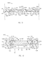
- FIG. 5 is a cross-sectional view of a single window sheet during the formation of a plurality of windows in accordance with the present invention.
- FIG. 6 is a cross-sectional view of a structure during the fabrication of a plurality of image sensor packages in accordance with the present invention.
- FIG. 7 is a cross-sectional view of the structure of FIG. 6 at a further stage of fabrication.
- FIG. 8A is a cross-sectional view of the structure of FIG. 7 at a further stage of fabrication in accordance with one embodiment of the present invention.
- FIG. 8B is a cross-sectional view of the structure of FIG. 7 at a further stage of fabrication in accordance with an alternative embodiment of the present invention.
- FIG. 9 is a cross-sectional view of the structure of FIG. 8B at a further stage of fabrication.
- FIGS. 10A and 10B are cross-sectional views of a structure during the fabrication of a plurality of image sensor packages in accordance with alternative embodiments of the present invention.
- FIG. 11 is a cross-sectional view of the structure of FIG. 10A or FIG. 10B at a further stage of fabrication.
- FIG. 12 is a cross-sectional view of a flip chip image sensor assembly in accordance with one embodiment of the present invention.
- FIG. 13 is a cross-sectional view of a leadframe image sensor assembly in accordance with an alternative embodiment of the present invention.
- FIG. 14 is a cross-sectional view of a wirebonded image sensor assembly in accordance with yet another alternative embodiment of the present invention.
- an image sensor package 100 (FIGS. 1 and 2) includes an image sensor 102 having bond pads 106 and an active area 104 on an upper surface 102 U of image sensor 102 .
- Image sensor package 100 further includes a window support 108 on upper surface 102 U of image sensor 102 .
- Window support 108 entirely encloses upper surface 102 U including active area 104 and bond pads 106 .
- a window 110 is in contact with window support 108 , window 110 overlying active area 104 .
- window support 108 and window 110 entirely enclose, and thus protect, active area 104 of image sensor 102 .
- radiation is directed at image sensor package 100 .
- This radiation passes through window 110 , passes through window support 108 , and strikes active area 104 of image sensor 102 , which responds to the radiation.
- Window 110 and window support 108 are transparent to the radiation.
- the refractive index of window support 108 is similar to the refractive index of window 110 . In this manner, the sensitivity of image sensor package 100 is improved compared to the prior art.
- window support 108 completely fills the region between window 110 and active area 104 .
- image sensor package 100 does not have a dew point.
- image sensor package 100 in accordance with present invention eliminates the need for a housing of the prior art. Accordingly, image sensor package 100 is significantly less expensive to manufacture than an image sensor assembly of the prior art.
- window 110 is attached directly to image sensor 102 by window support 108 , image sensor package 100 can be made relatively thin compared to a prior art image sensor assembly.
- a method of forming an image sensor package includes forming a window support layer 650 (FIG. 6) on an upper surface 602 U of an image sensor substrate 602 such as a wafer.
- Image sensor substrate 602 includes image sensors 102 having active areas 104 covered by window support layer 650 .
- an interior surface 500 I of a window sheet 500 is pressed into window support layer 650 such that windows 110 of window sheet 500 are above active areas 104 of image sensors 102 .
- window support layer 650 is a bonding material, e.g., an epoxy.
- Window support layer 650 is then setup, e.g., cured, gelled or made tacky.
- window sheet 500 is mounted to window support layer 650 .
- a series of shallow cuts 504 are made in interior surface 500 I of window sheet 500 to define and delineate windows 110 of window sheet 500 .
- Shallow cuts 504 in combination with window support layer 650 define cavities 710 (FIG. 7) above bond pads 106 of image sensors 102 of image sensor substrate 602 .
- Window sheet 500 is cut with a sawblade 802 A (FIG. 8B) from an exterior surface 500 E of window sheet 500 to singulate windows 110 from one another.
- Window sheet 500 is cut from exterior surface 500 E directly opposite of cavities 710 above bond pads 106 .
- the depth to which sawblade 802 A cuts below exterior surface 500 E is set to be sufficiently deep to insure that sawblade 802 A cuts all the way through window sheet 500 , yet is set to be sufficiently shallow to insure that sawblade 802 A does not damage bond pads 106 .
- cavities 710 accommodate, tolerance during this cutting of window sheet 500 .
- Image sensor substrate 602 is then singulated to form a plurality of image sensor packages 100 (FIGS. 1 and 2 ).
- active areas 104 of image sensors 102 are protected by windows 110 during singulation. More particularly, windows 110 protect active areas 104 from contamination and scratching during singulation, e.g., from silicon shards. As a result, damage or destruction of image sensors 102 is avoided. Accordingly, yield is increased and package cost is reduced compared to the prior art.
- windows 110 protect active areas 104 during subsequent processing of image sensor package 100 , e.g., during subsequent wire bonding and/or encapsulation and/or molding. More particularly, windows 110 protect active areas 104 from dust and contamination. Accordingly, after attachment of windows 110 to image sensors 102 , image sensor packages 100 can be stored or further packaged in any facility with or without a cleanroom.
- image sensor package 100 is further packaged.
- image sensor package 100 can be further packaged using any one of a number of conventional packaging techniques. For example, image sensor package 100 is put into a flip chip image sensor assembly as shown in FIG. 12, a leadframe image sensor assembly as shown in FIG. 13, or a wirebonded image sensor assembly as shown FIG. 14 .
- FIG. 1 is a perspective view, partially cutaway, of an image sensor package 100 (hereinafter package 100 ) in accordance with the present invention.
- FIG. 2 is a cross-sectional view of package 100 along the line II—II of FIG. 1 .
- package 100 includes an image sensor 102 , sometimes called a sensor device.
- Image sensor 102 includes an active area 104 , sometimes called an image array.
- Active area 104 is on an upper, e.g., first, surface 102 U of image sensor 102 .
- active area 104 is responsive to radiation, e.g., electromagnetic radiation, as is well known to those of skill in the art.
- active area 104 is responsive to infrared radiation, ultraviolet light, and/or visible light.
- image sensor 102 is a CMOS image sensor device, a charge coupled device (CCD), a pyroelectric ceramic on CMOS device, or an erasable programmable read-only memory device (EPROM) although other image sensors are used in other embodiments.
- CCD charge coupled device
- EPROM erasable programmable read-only memory
- Image sensor 102 further includes a plurality of bond pads 106 on upper surface 102 U of image sensor 102 .
- Bond pads 106 are connected to the internal circuitry of image sensor 102 .
- Active area 10 is inwards of bond pads 106 .
- window support 108 Formed on upper surface 102 U is a window support 108 . More particularly, window support 108 entirely contacts and entirely encloses upper surface 102 U including active area 104 and bond pads 106 . Sides 108 S of window support 108 are coplanar with sides 102 S of image sensor 102 .
- window support 108 is transparent to the radiation of interest, e.g., to the radiation to which active area 104 of image sensor 102 is responsive, as those of skill in the art will understand.
- window support 108 is an epoxy which has been setup, e.g., cured, gelled or made tacky.
- window support 108 is mastersil product grade 151 silicone epoxy available from Master Bond Inc. of Hackensack, N.J.
- Window support 108 is in contact with and secures a window 110 to upper surface 102 U of image sensor 102 .
- Window 110 includes an interior, e.g., first, surface 110 I and an exterior, e.g., second, surface 110 E opposite interior surface 110 I. Interior surface 110 I is secured to window support 108 and exterior surface 110 E is exposed to the ambient environment. Window 110 further includes sides 110 S, which extend between exterior surface 110 E and interior surface 110 I.
- window support 108 contacts interior surface 110 I only, i.e., does not contact sides 110 S. Further, window 110 overlies a central region CR of upper surface 102 U inwards of bond pads 106 and does not overlie bond pads 106 . Bond pads 106 are along the entire periphery of upper surface 102 U. Active area 104 is within central region CR and window 110 overlies active area 104 .
- Window 110 is parallel to upper surface 102 U of image sensor 102 . More particularly, a plane defined by interior surface 110 I (or exterior surface 110 E) is parallel to a plane defined by upper surface 102 U of image sensor 102 .
- Window 110 is transparent to the radiation of interest, e.g., to the radiation to which active area 104 of image sensor 102 is responsive, as those of skill in the art will understand.
- window 110 is optically transparent borosilicate glass.
- window support 108 and window 110 are sufficient to allow the necessary minimum amount of radiation needed for the proper operation of image sensor 102 to pass through window support 108 and window 110 .
- active area 104 of image sensor 102 transmits radiation such as electromagnetic radiation.
- image sensor 102 is a light emitting diode (LED) micro-display.
- radiation transmitted by active area 104 passes through window support 108 , through window 110 , and emanates from package 100 .
- active area 104 as a receiver of radiation is set forth.
- active area 104 is a receiver of radiation, a transmitter of radiation, or a transceiver, i.e., a transmitter and a receives, of radiation.
- the refractive index of window support 108 is similar to the refractive index of window 110 . In this manner, the sensitivity of package 100 is improved compared to the prior art.
- a housing was mounted around the image sensor and to the printed circuit mother board. This housing supported a window above the image sensor. However, located between the window and the image sensor was air. Disadvantageously, air has a relatively low refractive index compared to the window.
- window 110 and window support 108 of package 100 have a similar refractive index.
- the difference between the refractive index of window 110 and the refractive index or window support 108 is such that the amount of radiation reflected at the interface of window 110 and window support 108 is one percent or less.
- window 110 has a refractive index of 1.52 and window support 108 has a refractive index of 1.40. Accordingly, the amount of reflected radiation is reduced compared to the prior art. This improves the sensitivity of package 100 compared to prior at image sensor assemblies. In one embodiment, package 100 is 13% more sensitive to electromagnetic radiation than prior art image sensor assemblies.
- package 100 is a cavityless package, i.e., package 100 does not have a cavity between window 110 and active area 104 .
- package 100 has no dew point.
- prior art image sensor assemblies had a dew point, i.e., a temperature at which condensation formed within the housing which enclosed the image sensor and supported the window.
- moisture had a tendency to condense within the housing and on the interior surface of the window.
- this condensation it was important to avoid subjecting the image sensor assembly to extreme low temperatures. Disadvantageously, this limited the temperature range over which the image sensor assembly would satisfactorily perform.
- the image sensor assembly was fabricated in a low humidity environment to avoid trapping moisture within the housing and was hermetically sealed by the housing to keep out moisture. This added complexity, which increased the cost of the image sensor assembly. Further, in the event that the hermetic seal of the housing failed, the image sensor was damaged or destroyed.
- package 100 does not have a dew point, package 100 operates satisfactorily over a broader range of temperatures and, more particularly, at lower temperatures than image sensor assemblies of the prior art. Further, since package 100 is a cavityless package, there is no possibility that moisture will leak into package 100 . Accordingly, the reliability of package 100 is greater than that of the prior art.
- package 100 in accordance with present invention eliminates the need for a housing of the prior art. Accordingly, package 100 is significantly less expensive to manufacture than image sensor assemblies of the prior art.
- window 110 is attached directly to image sensor 102 by window support 108 , package 100 can be made relatively thin compared to a prior art image sensor assembly. To illustrate, a 0.039 inch (1.0 mm) or less thickness for package 100 is easily achievable.
- the prior art image sensor housing was relatively bulky and extended upwards from the printed circuit mother board a significant distance, e.g., 0.100 inches (2.54 mm) to 0.120 inches (3.05 mm) or more. Since package 100 can be made relatively thin, package 100 is well suited for use with miniature lightweight electronic devices, which require thin and lightweight image sensor assemblies.
- window support 108 entirely encloses upper surface 102 U including bond pads 106 , i.e., window support 108 covers bond pads 106 .
- bond wire or other electrically conductive structures are electrically connected to bond pads 106 .
- FIG. 3 is a cross-sectional view of an image sensor package 100 A (hereinafter package 100 A) having exposed bond pads 106 in accordance with an alternative embodiment of the present invention.
- Package 100 A of FIG. 3 is similar to package 100 of FIGS. 1 and 2 and only the significant differences are discussed below.
- package 100 A includes a window support 302 .
- Window support 302 is formed on central region CR of upper surface 102 U of image sensor 102 .
- Window support 302 contacts and entirely encloses active area 104 yet does not extend over bond pads 106 . Since bond pads 106 are exposed, bond wires or other electrically conductive structures are readily connected to bond pads 106 .
- window support 302 is transparent to the radiation of interest.
- window support 302 is formed of the same material as window support 108 (FIGS. 1, 2 ) described above.
- FIG. 4 is an enlarged cross-sectional view of the region IV of package 100 of FIG. 2 .
- window 110 includes a locking feature 400 along the periphery of window 110 .
- locking feature 400 mechanically locks window 110 to the package body, e.g., to plastic or liquid encapsulant, as discussed in greater detail below in reference to FIGS. 12, 13 and 14 .
- Locking feature 400 is formed along sides 110 S (FIGS. 1, 2 ) of window 110 .
- locking feature 400 is shaped as a ledge, sometimes called a step, which extends around the periphery of window 110 .
- locking feature 400 includes a rectangular ring-like shelf 402 , e.g., a third surface, which extends around exterior surface 110 E. Shelf 402 is located on a plane parallel to, and located between, a plane defined by exterior surface 110 E and a plane defined by interior surface 100 I.
- Step sides 404 extend between exterior surface 110 E and shelf 402 and step sides 406 extend between shelf 402 and interior surface 110 I.
- step sides 404 , 406 are perpendicular to planes defined by exterior surface 110 E, interior surface 110 I, and shelf 402 .
- shelf 402 and step sides 494 define a pocket 408 .
- the package body extends into and fills pocket 408 thus mechanically locking window 110 into place.
- locking feature 400 is illustrated as a ledge in FIG. 4, in light of this disclosure, those of skill in the art will understand that other locking features can be used. Further, in one embodiment, window 110 does not include a locking feature.
- window 110 is fabricated simultaneously with a plurality of windows 110 from a single window sheet.
- FIG. 5 is a cross-sectional view of a single window sheet 500 during the formation of a plurality of windows 110 including a first window 110 A and a second window 110 B.
- window sheet 500 is a sheet of borosilicate glass.
- window sheet 500 is attached to a support 502 such as a sticky tape used in wafer dicing as is well known to those of skill in the art.
- a series of shallow cuts 504 are made in an interior, e.g., first, surface 500 I of window sheet 500 , for example, with a saw blade, to define and delineate windows 110 .
- a first shallow cut 504 A of the plurality of shallow cuts 504 defines and delineates first window 110 A from second window 110 B.
- An exterior, e.g., second, surface 500 E of window sheet 500 is attached to support 502 .
- shallow cut 504 A only score window sheet 500 and does not cut through window sheet 500 .
- shallow cut 504 A is a rectangular groove 0.015 inches (0.38 mm) wide, which cuts halfway through window sheet 500 . More generally, shallow cut 504 A has a width W 1 .
- the other shallow cuts 504 are similar to shallow cut 504 A.
- the other windows 110 are similarly defined and delineated from adjacent windows 110 by corresponding shallow cuts 504 .
- windows 110 are formed in an array, e.g., a 2 ⁇ 2, 3 ⁇ 3, . . . or nxm array.
- FIG. 6 is a cross-sectional view of a structure 600 during the fabrication of a plurality of packages 100 (FIGS. 1, 2 ) in accordance with the present invention.
- Structure 600 includes an image sensor substrate 602 such as a silicon wafer.
- Image sensor substrate 602 includes a plurality of image sensors 102 integrally connected together.
- Image sensors 102 include active areas 104 formed on an upper, e.g., first, surface 602 U of image sensor substrate 602 .
- Image sensors 102 further include bond pads 106 on upper surface 602 U of image sensor substrate 602 . Bond pads 106 are connected to the internal circuitry of image sensors 102 .
- a first image sensor 102 A of the plurality of image sensors 102 includes a first active area 104 A of the plurality of active areas 104 .
- Image sensor 102 A also includes a first bond pad 106 A of the plurality of bond pads 106 .
- the other image sensors 102 include active areas 104 and bond pads 106 in a similar manner.
- Image sensors 102 are integrally connected together in an array format. Each of image sensors 102 is delineated by a singulation street 604 , which is located between adjacent image sensors 102 .
- a first singulation street 604 A of the plurality of singulation streets 604 delineates first image sensor 102 A from a second image sensor 102 B of the plurality of image sensors 102 .
- the other image sensors 102 are similarly delineated from adjacent image sensors 102 by corresponding singulation streets 604 .
- a window support layer 650 is formed on an upper, e.g., first, surface 602 U of image sensor substrate 602 .
- upper surface 602 U is coated with a bonding material, e.g., an epoxy, such as mastersil product grade 151 silicone epoxy available from Master Bond Inc. of Hackensack, N.J. to form window support layer 650 .
- Upper surface 602 U is coated with the bonding material using any one of a number of techniques, e.g., a spin coating, syringe dispensing and/or screen printing technique, as those of skill in the art will understand.
- it is important that a well-defined, controlled, and repeatable volume of the bonding material is coated on upper surface 602 U.
- window support layer 650 entirely covers and encloses upper surface 602 U of image sensor substrate 602 . More particularly, window support layer 650 extends over and covers bond pads 106 , active areas 104 and upper surfaces 102 U of image sensors 102 .
- FIG. 7 is a cross-sectional view of structure 600 of FIG. 6 at a further stage of fabrication.
- window sheet 500 is removed from support 502 , inverted and pressed into window support layer 650 .
- window sheet 500 is pressed into window support layer 650 while window support layer 650 is wet, i.e., before window support layer 650 is setup.
- window support layer 650 is cured.
- window support layer 650 is cured with ultraviolet light or heat.
- window support layer 650 can be gelled or made tacky.
- window support layer 650 is setup, e.g., cured, gelled or made tacky.
- window support layer 650 which ultimately forms window supports 108 , can be formed with less structural integrity and adhesion to windows 110 than otherwise would be required if window support 108 were entirely responsible for supporting windows 110 .
- window sheet 500 is aligned with image sensor substrate 602 such that shallow cuts 504 are aligned with corresponding singulation streets 604 and corresponding bond pads 106 .
- cavities 710 are formed by shallow cuts 504 and window support layer 650 . Cavities 710 are located above, i.e., in a first direction from, singulation streets 604 and adjacent bond pads 106 .
- image sensor 102 A includes bond pad 106 A.
- Image sensor 102 B includes a second bond pad 106 B of the plurality of bond pads 106 .
- Bond pads 106 A, 106 B are formed directly adjacent to singulation street 604 A and are opposite one another relative to singulation street 604 A.
- a first cavity 710 A of the plurality of cavities 710 is formed by shallow groove 504 A and window support layer 650 . Cavity 710 A is above singulation street 604 A and bond pads 106 A, 106 B.
- windows 110 of window sheet 500 are in contact with window support layer 650 , which supports windows 110 above corresponding active areas 104 .
- window 110 A is in contact with window support layer 650 , which supports window 110 A above active area 104 A.
- Cavities 710 are located between window sheet 500 and bond pads 106 and singulation streets 604 . Of importance, cavities 710 accommodate tolerance in removal, e.g., sawing, of window sheet 500 above bond pads 106 and singulation streets 604 as discussed in greater detail below with reference to FIGS. 8A, 8 B.
- FIG. 8A is a cross-sectional view of structure 600 of FIG. 7 at a further stage of fabrication in accordance with one embodiment of the present invention.
- window sheet 500 is cut from exterior surface 500 E to singulate windows 110 from one another.
- Window sheet 500 is cut by a sawblade 802 , although in other embodiments, window sheet 500 is cut using a different technique, e.g., by a laser.
- Window sheet 500 is cut from exterior surface 500 E directly opposite of cavities 710 and above singulation streets 604 and bond pads 106 . Window sheet 500 is cut all the way through to cavities 710 .
- the depth to which sawblade 802 cuts below exterior surface 500 E is set to be sufficiently deep to insure that sawblade 802 cuts all the way through window sheet 500 , yet is set to be sufficiently shallow to insure that sawblade 802 does not damage bond pads 106 and, more generally, image sensor substrate 602 .
- cavities 710 accommodate tolerance during cutting of window sheet 500 .
- Width W 2 of sawblade 802 is approximately the same as width W 1 of shallow cuts 504 .
- windows 110 are formed to have planar, i.e., flat, sides 110 S.
- sawblade 802 is illustrated as cutting through window sheet 500 from exterior surface 500 E between window 110 A and window 110 B.
- Sawblade 802 cuts all the way through window sheet 500 to cavity 710 A (FIG. 7) above bond pad 106 A, bond pad 106 B and singulation street 604 A thus singulating window 110 A from window 110 B.
- Sawblade 802 singulates the other windows 110 in a similar manner.
- windows 110 are formed to have planar sides 110 S.
- FIG. 8B is a cross-sectional view of structure 600 of FIG. 7 at a further stage of fabrication in accordance with an alternative embodiment of the present invention.
- FIG. 8B is substantially similar to FIG. 8 A and only the significant differences are discussed below.
- window sheet 500 is cut from exterior surface 500 E to singulation windows 110 from one another.
- Window sheet 500 is cut by a sawblade 802 A, although in other embodiments, window sheet 500 is cut using a different technique, e.g., by a laser.
- Window sheet 500 is cut from exterior surface 500 E directly opposite of cavities 710 and above singulation streets 604 and bond pads 106 . Window sheet 500 is cut all the way through to cavities 710 .
- Width W 3 of sawblade 802 A is greater than width W 1 of shallow cuts 504 .
- windows 110 are formed to have locking features 400 as discussed in detail above with reference to FIG. 4 .
- sawblade 802 A is illustrated as cutting through window sheet 500 from exterior surface 500 E between window 110 A and window 110 B.
- Sawblade 802 A cuts all the way through window sheet 500 to cavity 710 A (FIG. 7) above bond pad 106 A, bond pad 106 B and singulation street 604 A thus singulating window 110 A from window 110 B.
- Width W 3 of sawblade 802 A is greater than width W 1 of shallow cuts 504 resulting in the formation of windows 110 A, 110 B having locking features 400 .
- Sawblade 802 A singulates the other windows 110 in a similar manner.
- shallow cuts 504 and the cuts made by sawblade 802 A in window sheet 500 are desirably rough cuts to enhance the locking ability of locking features 400 . Since rough cuts are desirable, shallow cuts 504 and the cuts made by sawblade 802 A can be made using a high-speed cutting process.
- windows 110 in accordance with the present invention are fabricated at a lower cost than windows of prior art image sensor assemblies.
- bond pads 106 and singulation streets 604 are laterally located between adjacent windows 110 and are not covered by windows 110 .
- bond pad 106 A, bond pad 106 B and singulation street 604 A are laterally located between window 110 A and window 110 B.
- bond pads 106 and singulation streets 604 remain covered by window support layer 650 .
- FIG. 9 is a cross-sectional view of structure 600 of FIG. 8B at a further stage of fabrication.
- window support layer 650 is selectively removed, sometimes called etched, above bond pads 106 and singulation streets 604 .
- windows 110 are used as an etch mask to selectively remove window support layer 650 laterally between windows 110 .
- Window support layer 650 is selectively removed using any one of a number of techniques, e.g., by chemical stripping or plasma etching, using windows 110 as an etch mask.
- window support layer 650 is removed laterally between window 110 A and window 110 B using window 110 A and window 110 B as an etch mask to expose bond pad 106 A, bond pad 106 B and singulation street 604 A. Window support layer 650 is selectively removed laterally between the other windows 110 in a similar manner.
- window supports 302 After being selectively removed, the remaining portions of window support layer 650 , i.e., the portions of window support layer 650 between windows 110 and corresponding image sensors 102 , form window supports 302 .
- a first window support 302 A of the plurality of window supports 302 is between window 110 A and image sensor 102 A.
- the other window supports 302 are formed in a similar manner.
- Image sensor substrate 602 is singulated along singulation streets 604 to form a plurality of packages 100 A (FIG. 3 ).
- window support layer 650 is not etched as shown in FIG. 9, e.g., structure 600 of FIG. 8B is singulated along singulation streets 604 to form a plurality of packages 100 (FIGS. 1 and 2 ).
- window support layer 650 forms window supports 108 of packages 100 .
- singulation is accomplished using any one of a number of conventional singulation techniques, e.g., by laser cutting or mechanical sawing through image sensor substrate 602 .
- package 100 of FIGS. 1 and 2 is frequently referred to and discussed below. However, it is understood that the discussion and illustrations equally apply to package 100 A of FIG. 3 .
- active areas 104 of image sensors 102 are protected by windows 110 during singulation of image sensor substrate 602 . More particularly, windows 110 protect active areas 104 from contamination and scratching during singulation, e.g., from silicon shards. As a result, damage or destruction of image sensors 102 is avoided. Accordingly, yield is increased and package cost is reduced compared to the prior art.
- windows 110 protect active areas 104 during subsequent processing of package 100 , e.g., during subsequent wire bonding and/or encapsulation and/or molding. More particularly, windows 110 protect active areas 104 from dust and contamination. Accordingly, after attachment of windows 110 to image sensors 102 , structure 600 and, after singulation of image sensor substrate 602 , packages 100 can be stored or further packaged in any facility with or without a cleanroom.
- the housing which hermetically sealed the image sensor, was mounted directly to the printed circuit mother board.
- the image sensor had to be carefully stored and packaged in a cleanroom. Since the prior art requirement carefully storing and packaging the image sensor in a cleanroom is eliminated, the cost associated with package 100 is reduced compared to the prior art.
- packages 100 can also be manufactured on an individual basis, if desired. For example, referring to FIGS. 1 and 2, window 110 is attached by window support 108 after image sensor 102 is die attached and/or wire bonded.
- window support layer 650 is selectively removed to expose bond pads 106 .
- window supports are selectively formed on active areas 104 .
- FIG. 10A is a cross-sectional view of a structure 1000 during the fabrication of a plurality of packages 100 A (FIG. 3) in accordance with an alternative embodiment of the present invention.
- Structure 1000 of FIG. 10A is similar to structure 600 of FIG. 6 and only the significant differences are discussed below.
- drops 1006 are applied to each active area 104 such that drops 1006 are on active areas 104 .
- a first drop 1006 A of the plurality of drops 1006 is applied to, and is on, active area 104 A.
- drop 1006 A is applied by pin transfer of a bonding material. More particularly, a pin is dipped in a bath of the bonding material, the pin is removed from the bath such that the tip of the pin is coated with the bonding material, and the tip of the pin is moved adjacent to active area 104 A. The bonding material is transferred from the tip of the pin to active area 104 A to form drop 1006 A.
- drop 1006 A is formed using a syringe and/or screen printing technique.
- the other drops 1006 are formed in a similar manner simultaneously or, alternatively, one at a time.
- drop 1006 A has an apex 1008 A near, or at, a horizontal center 1010 A of drop 1006 A.
- the other drops 1006 have corresponding apexes 1008 near corresponding horizontal centers 1010 in a similar manner.
- FIG. 11 is a cross-sectional view of structure 1000 of FIG. 10A (or FIG. 10B) at a further stage of fabrication in accordance with the present invention.
- interior surface 500 I of window sheet 500 is pressed into drops 1006 to form window supports 302 .
- windows 110 of window sheet 500 are pressed into corresponding drops 1006 to form corresponding window supports 302 .
- window 110 A of window sheet 500 is pressed into drop 1006 A to form window support 302 A.
- drop 1006 A is formed to have an apex 1008 A
- window 110 A initially contacts apex 1008 A.
- drop 1006 A is squeezed by window 110 A downwards, e.g., in a first direction, towards active area 104 A and outwards from apex 1008 A. Squeezing drop 1006 A in this manner avoids bubble formation, i.e., avoids entrapment of air under window 110 A and within window support 302 A. These bubbles would otherwise distort radiation passing through window support 302 A.
- drop 1006 A has a volume sufficient to have window support 302 A entirely cover active area 104 A of image sensor 102 A after window sheet 500 is pressed into place. However, drop 1006 A has a volume insufficient to have window support 302 A extend over any of bond pads 106 . In one embodiment, drop 1006 A is formed within active area 104 A and is squeezed such that window support 302 A entirely covers active area 104 A after window sheet 500 is pressed into place.
- window 110 A is placed into drop 1006 A, it is understood that the other windows 110 are placed into the other corresponding drops 1006 to form the other corresponding window supports 302 in a similar manner simultaneously.
- drops 1006 are applied to window sheet 500 .
- drops 1006 are applied to corresponding active areas 104 or, alternatively, to corresponding windows 110 , and are squeezed between active areas 104 and corresponding windows 110 to form corresponding window supports 302 .
- FIG. 10B is a cross-sectional view of a structure 1000 A in accordance with this alternative embodiment of the present invention.
- drops 1006 are applied to each window 110 of window sheet 500 such that drops 1006 are on windows 110 .
- a first drop 1006 A of the plurality of drops 1006 is applied to, and is on, window 110 A.
- Drop 1006 A is applied to window sheet 500 in a similar manner to that described above in reference to the application of drop 1006 A to active area 104 A to FIG. 10 A.
- the other drops 1006 are formed in a similar manner simultaneously or, alternatively, one at a time.
- drop 1006 A has an apex 1008 A near, or at, a horizontal center 1010 A of drop 1006 A.
- the other drops 1006 have corresponding apexes 1008 near corresponding horizontal centers 1010 in a similar manner.
- Drops 1006 are pressed into corresponding active areas 104 to form corresponding window supports 302 .
- window sheet 500 is moved towards image sensor substrate 602 to press drops 1006 into corresponding active areas 104 .
- drop 1006 A is pressed into active area 104 A to form window support 302 A.
- active area 104 A initially contacts apex 1008 A.
- drop 1006 A is pressed into active area 104 A, drop 1006 A in squeezed by active area 104 A upwards, e.g., in a second direction, towards window 110 A and outwards from apex 1008 A. Squeezing drop 1006 A in this manner avoids bubble formation, i.e., avoids entrapment of air above active area 104 A and within window support 302 A.
- drop 1006 A has a volume sufficient to have window support 302 A entirely cover active area 104 A of image sensor 102 A after window sheet 500 is pressed into place. However drop 1006 A has a volume insufficient to have window support 302 A extend over any of bond pads 106 .
- window supports 302 are setup.
- Window sheet 500 is cut to singulated windows 110 in a manner similar to that illustrated and described above in reference to FIG. 8A or FIG. 8B, with the exception being that cavities 710 are now formed by shallow cuts 504 , window supports 302 and upper surface 602 U of image sensor substrate 602 .
- Image sensor substrate 602 is singulated along singulation streets 604 to form a plurality of packages 100 A (FIG. 3 ).
- windows 110 are essentially parallel to upper surfaces 102 U of image sensors 102 . Further, a distance ZH, sometimes called the Z height, between windows 110 and image sensors 102 is precisely controlled to within tight tolerance.
- the window was placed on a shelf of the housing after the housing was fabricated. Since a significant tolerance was associated with the window placement, the distance between the window and the image sensor had significant variations from assembly to assembly. However, to insure optimum operation of the image sensor, it is important that the distance between the window and the image sensor be precise. Since the tolerance in this distance is reduced in packages 100 and 100 A (FIGS. 2 and 3, respectively), the performance of packages 100 and 100 A is superior to that of the prior art.
- window sheet 500 is singulated to form a plurality of individual windows 110 , which are individually pressed into window support layer 650 (FIG. 7) or into drops 1006 (FIG. 11) sequentially or, alternatively, simultaneously.
- package 100 (FIG. 2) is further packaged.
- package 100 can be further packaged using any one of a number of conventional packaging techniques, e.g., standard molding and/or liquid encapsulation techniques.
- package 100 is put into a flip chip image sensor assembly such as that illustrated in FIG. 12, a leadframe image sensor assembly such as that illustrated in FIG. 13 or a wirebonded image sensor assembly such as that illustrated in FIG. 14 .
- FIG. 12 is a cross-sectional view of a flip chip image sensor assembly 1200 (hereinafter assembly 1200 ) in accordance with one embodiment of the present invention.
- assembly 1200 includes a substrate 1202 .
- substrate 1202 is a printed circuit board or, alternatively, is tape, as those of skill in the art will understand.
- Substrate 1202 includes a plurality of electrically conductive traces 1204 formed on a lower, e.g., first, surface 1202 L of substrate 1202 .
- Bond pads 106 are electrically connected to corresponding traces 1204 by corresponding electrically conductive bumps 1206 .
- Traces 1204 are electrically connected to corresponding electrically conductive vias 1208 which extend from lower surface 1202 L to an upper, e.g., second, surface 1202 U of substrate 1202 opposite lower surface 1202 L.
- Vias 1208 are electrically connected to corresponding electrically conductive traces 1210 on upper surface 1202 U of substrate 1202 .
- Formed on traces 1210 are corresponding electrically conductive pads 1212 .
- Formed on pads 1212 are corresponding electrically conductive interconnection balls 1214 such as solder balls. Interconnection balls 1214 are used to electrically connect assembly 1200 to a larger substrate (not shown) such as a printed circuit mother board.
- a first bond pad 106 A of the plurality of bond pads 106 is electrically connected to a first trace 1204 A of the plurality of traces 1204 by a first bump 1206 A of the plurality of bumps 1206 .
- Trace 1204 A is electrically connected to a first via 1208 A of the plurality of vias 1208 .
- Via 1208 A is electrically connected to a first trace 1210 A of the plurality of traces 1210 .
- a first pad 1212 A of the plurality of pads 1212 is formed on trace 1210 A. Formed on pad 1212 A is a first interconnection ball 1214 A of the plurality of interconnection balls 1214 .
- an electrically conductive pathway between bond pad 106 A and interconnection ball 1214 A is formed by bump 1206 A, trace 1204 A, via 1208 A, trace 1210 A and pad 1212 A.
- the other bond pads 106 , bumps 1206 , traces 1204 , vias 1208 , traces 1210 , pads 1212 and interconnection balls 1214 are electrically connected to one another in a similar fashion so are not discussed further to avoid detracting from the principals of the invention.
- substrate 1202 is a multi-layered laminated substrate and, instead of straight-through vias 1208 , a plurality of electrically conductive traces on various layers in substrate 1202 are interconnected by a plurality of electrically conductive vias to form the electrical interconnections between traces 1204 and 1210 .
- interconnection balls 1214 are distributed in an array format to form a ball grid array (BGA) package.
- interconnection balls 1214 are not formed, e.g., to form a metal land grid array (LGA) package or a leadless chip carrier (LCC) package.
- BGA ball grid array
- LGA metal land grid array
- LCC leadless chip carrier
- Substrate 1202 includes a central aperture 1216 .
- Window 110 is located within, or is located adjacent to, central aperture 1216 .
- exterior surface 110 E of window 110 is exposed through aperture 1216 .
- radiation is directed at assembly 1200 . This radiation passes through window 110 , through window support 108 , and strikes active area 104 . Active area 104 responds to this radiation as is well known to those of skill in the art.
- Assembly 1200 further includes a package body 1218 .
- Package body 1218 is an electrically insulating material and electrically protects, e.g., prevents shorting of, and environmentally protects, e.g., from moisture, the various electrically conductive structures of assembly 1200 .
- package body 1218 provides mechanical strength to assembly 1200 and, in particular, minimizes failure of bumps 1206 and the associated detachment of image sensor 102 from substrate 1202 .
- package body 1218 encloses sides 102 S of image sensor 102 , lower surface 1202 L and central aperture 1216 of substrate 1202 , traces 1204 , and window support 108 . Further, package body 1218 , in combination with window support 108 , mechanically locks window 110 in place.
- package body 1218 includes an exterior locking feature 1220 , which fills pocket 408 of window 110 , thus mechanically locking window 110 in place.
- package body 1218 including exterior locking feature 1220 is integral, i.e., is one piece and not a plurality of single pieces connected together. In this embodiment, package body 1218 leaves exposed exterior surface 110 E of window 110 , i.e., package body 1218 does not contact or cover exterior surface 110 E.
- Package body 1218 is formed of any one of a number of conventional packaging materials.
- package body 1218 is formed from a plastic encapsulant or, alternatively, a liquid encapsulant.
- FIG. 13 is a cross-sectional view of a leadframe image sensor assembly 1300 (hereinafter assembly 1300 ) in accordance with an alternative embodiment of the present invention.
- assembly 1300 a lower, e.g., second, surface 102 L of image sensor 102 is attached to a die attach pad 1302 of a leadframe 1304 .
- lower surface 102 L is attached to die attach pad 1302 with adhesive 1306 .
- Leadframe 1304 further includes a plurality of leads 1308 .
- Bond pads 106 are electrically connected to corresponding leads 1308 by corresponding bond wires 1310 .
- a first bond pad 106 A of the plurality of bond pads 106 is electrically connected to a first lead 1308 A of the plurality of leads 1308 by a first bond wires 1310 A of the plurality of bond wires 1310 .
- the other bond pads 106 are electrically connected to the other corresponding leads 1308 by the other corresponding bond wires 1310 in a similar fashion so are not discussed further.
- Assembly 1300 further includes a package body 1312 .
- Package body 1312 is an electrically insulating material and electrically protects, e.g., prevents shorting of, and environmentally protects, e.g., from moisture, the various electrically conductive structures of assembly 1300 .
- Package body 1312 encloses sides 102 S of image sensor 102 , bond wires 1310 , die attach pad 1302 , inner ends 1308 I of leads 1308 , and window support 108 . Further, package body 1312 , in combination with window support 108 , mechanically locks window 110 in place. In particular, package body 1312 includes an exterior locking feature 1314 which fills pocket 408 of window 110 , thus mechanically locking window 110 in place. In one embodiment, package body 1312 including exterior locking feature 1314 is integral. In this embodiment, package body 1312 leaves exposed exterior surface 110 E of window 110 , i.e., package body 1312 does not contact or cover exterior surface 110 E.
- Package body 1312 is formed of any one of a number of conventional packaging materials.
- package body 1312 is formed from a plastic encapsulant or, alternatively, a liquid encapsulant.
- FIG. 14 is a cross-sectional view of a wirebonded image sensor assembly 1400 (hereinafter assembly 1400 ) in accordance with yet another alternative embodiment of the present invention.
- assembly 1400 includes a substrate 1402 .
- substrate 1402 is a printed circuit board, ceramic, or tape, although other materials are used in other embodiments.
- Lower surface 102 L of image sensor 102 is attached to an upper, e.g., first, surface 1402 U of substrate 1402 , for example, with adhesive 1430 .
- Substrate 1402 includes a plurality of electrically conductive traces 1404 formed on upper surface 1402 U of substrate 1402 .
- Bond pads 106 are electrically connected to corresponding traces 1404 by corresponding electrically conductive bond wires 1406 .
- Traces 1404 are electrically connected to corresponding electrically conductive vias 1408 which extend from upper surface 1402 U to a lower, e.g., second, surface 1402 L of substrate 1402 opposite upper surface 1402 U.
- Vias 1408 are electrically connected to corresponding electrically conductive traces 1410 on lower surface 1402 L of substrate 1402 .
- Formed on traces 1410 are corresponding electrically conductive pads 1412 .
- Formed on pads 1412 are corresponding electrically conductive interconnection balls 1414 such as solder balls. Interconnection balls 1414 are used to electrically connect assembly 1400 to a larger substrate (not shown) such as a printed circuit mother board.
- a first bond pad 106 A of the plurality of bond pads 106 is electrically connected to a first trace 1404 A of the plurality of traces 1404 by a first bond wire 1406 A of the plurality of bond wires 1406 .
- Trace 1404 A is electrically connected to a first via 1408 A of the plurality of vias 1408 .
- Via 1408 A is electrically connected to a first trace 1410 A of the plurality of traces 1410 .
- a first pad 1412 A of the plurality of pads 1412 is formed on trace 1410 A. Formed on pad 1412 A is a first interconnection ball 1414 A of the plurality of interconnection balls 1414 .
- an electrically conductive pathway between bond pad 106 A and interconnection ball 1414 A is formed by bond wire 1406 A, trace 1404 A, via 1408 A, trace 1410 A and pad 1412 A.
- the other bond pads 106 , bond wires 1406 , traces 1404 , vias 1408 , traces 1410 , pads 1412 and interconnection balls 1414 are electrically connected to one another in a similar fashion so are not discussed further to avoid detracting from the principals of the invention.
- substrate 1402 is a multi-layered laminated substrate and, instead of straight-through vias 1408 , a plurality of electrically conductive traces on various layers in substrate 1402 are interconnected by a plurality of electrically conductive vias to form the electrical interconnections between traces 1404 and 1410 .
- interconnection balls 1414 are distributed in an array format to form a ball grid array (BGA) package.
- interconnection balls 1414 are not formed, e.g., to form a metal land grid array (LGA) package or a leadless chip carrier (LCC) package.
- BGA ball grid array
- LGA metal land grid array
- LCC leadless chip carrier
- Assembly 1400 further includes a package body 1418 .
- Package body 1418 is an electrically insulating material and electrically protects, e.g., prevents shorting of, and environmentally protects, e.g., from moisture, the various electrically conductive structures of assembly 1400 .
- package body 1418 encloses sides 102 S of image sensor 102 , upper surface 1402 U of substrate 1402 , traces 1404 , bond wires 1406 and window support 108 . Further, package body 1418 , in combination with window support 108 , mechanically locks window 110 in place.
- package body 1418 includes an exterior locking feature 1420 which fills pocket 408 of window 110 , thus mechanically locking window 110 in place.
- package body 1418 including exterior locking feature 1420 is integral. In this embodiment, package body 1418 leaves exposed exterior surface 110 E of window 110 , i.e., package body 1418 does not contact or cover exterior surface 110 E.
- Package body 1418 is formed of any one of a number of conventional packaging materials.
- package body 1418 is formed from a plastic encapsulant or, alternatively, a liquid encapsulant.
- FIGS. 12, 13 and 14 are examples of image sensor assemblies, which incorporate package 100 in accordance with present invention.
- bond wires 1310 , 1406 respectively, break through window support 108 to bond pads 106 from heat and mechanical energy during the wire bonding process.
- package 100 A (FIG. 3) having exposed bond pads 106 is used in place of package 100 .
- solder masks can be applied to upper surface 1202 U and/or lower surface 1202 L of substrate 1202 (FIG. 12) and/or upper surface 1402 U and/or lower surface 1402 L of substrate 1402 (FIG. 14 ).
Abstract
Description
Claims (18)
Priority Applications (2)
| Application Number | Priority Date | Filing Date | Title |
|---|---|---|---|
| US09/610,314 US6407381B1 (en) | 2000-07-05 | 2000-07-05 | Wafer scale image sensor package |
| TW090108700A TW501243B (en) | 2000-07-05 | 2001-04-11 | Wafer scale image sensor package |
Applications Claiming Priority (1)
| Application Number | Priority Date | Filing Date | Title |
|---|---|---|---|
| US09/610,314 US6407381B1 (en) | 2000-07-05 | 2000-07-05 | Wafer scale image sensor package |
Publications (1)
| Publication Number | Publication Date |
|---|---|
| US6407381B1 true US6407381B1 (en) | 2002-06-18 |
Family
ID=24444533
Family Applications (1)
| Application Number | Title | Priority Date | Filing Date |
|---|---|---|---|
| US09/610,314 Expired - Lifetime US6407381B1 (en) | 2000-07-05 | 2000-07-05 | Wafer scale image sensor package |
Country Status (1)
| Country | Link |
|---|---|
| US (1) | US6407381B1 (en) |
Cited By (104)
| Publication number | Priority date | Publication date | Assignee | Title |
|---|---|---|---|---|
| US6528857B1 (en) | 2000-11-13 | 2003-03-04 | Amkor Technology, Inc. | Chip size image sensor bumped package |
| US6531333B2 (en) * | 2000-04-05 | 2003-03-11 | Hong-Ming Lin | Chip photoelectric sensor assembly and method for making same |
| US20030071341A1 (en) * | 2001-10-16 | 2003-04-17 | Jeung Boon Suan | Apparatus and method for leadless packaging of semiconductor devices |
| US6620646B1 (en) * | 2000-11-13 | 2003-09-16 | Amkor Technology, Inc. | Chip size image sensor wirebond package fabrication method |
| US6629633B1 (en) | 2000-11-13 | 2003-10-07 | Amkor Technology, Inc. | Chip size image sensor bumped package fabrication method |
| US20030213124A1 (en) * | 2002-03-27 | 2003-11-20 | Jason Chuang | Method for packaging image sensors |
| US6660559B1 (en) | 2001-06-25 | 2003-12-09 | Amkor Technology, Inc. | Method of making a chip carrier package using laser ablation |
| WO2004008522A2 (en) * | 2002-07-16 | 2004-01-22 | Austriamicrosystems Ag | Method for producing a component having submerged connecting areas |
| EP1387397A2 (en) * | 2002-07-29 | 2004-02-04 | Fuji Photo Film Co., Ltd. | Solid-state imaging device and method of manufacturing the same |
| US20040031621A1 (en) * | 2002-08-19 | 2004-02-19 | Heng Puah Kia | Packaged microelectronic component assemblies |
| US20040035917A1 (en) * | 2002-08-22 | 2004-02-26 | Michel Koopmans | Apparatus and method for depositing and reflowing solder paste on a microelectronic workpiece |
| US20040041271A1 (en) * | 2002-08-29 | 2004-03-04 | Storli Farrah J. | Methods for wafer-level packaging of microelectronic devices and microelectronic devices formed by such methods |
| US20040053447A1 (en) * | 2001-06-29 | 2004-03-18 | Foster Donald Craig | Leadframe having fine pitch bond fingers formed using laser cutting method |
| US20040077121A1 (en) * | 2002-04-22 | 2004-04-22 | Hiroshi Maeda | Solid-state imaging device and method of manufacturing said solid-state imaging device |
| US6750547B2 (en) | 2001-12-26 | 2004-06-15 | Micron Technology, Inc. | Multi-substrate microelectronic packages and methods for manufacture |
| US6762074B1 (en) | 2003-01-21 | 2004-07-13 | Micron Technology, Inc. | Method and apparatus for forming thin microelectronic dies |
| US20040178495A1 (en) * | 2003-03-14 | 2004-09-16 | Yean Tay Wuu | Microelectronic devices and methods for packaging microelectronic devices |
| US20040214373A1 (en) * | 2003-04-22 | 2004-10-28 | Tongbi Jiang | Packaged microelectronic devices and methods for packaging microelectronic devices |
| US20040214372A1 (en) * | 2003-04-07 | 2004-10-28 | Walter Moden | Method for fabricating image sensor semiconductor package |
| US20040238909A1 (en) * | 2003-05-30 | 2004-12-02 | Boon Suan Jeung | Packaged microelectronic devices and methods of packaging microelectronic devices |
| US20050063033A1 (en) * | 2003-09-18 | 2005-03-24 | Kinsman Larry D. | Microelectronic devices and methods for packaging microelectronic devices |
| US20050073018A1 (en) * | 2003-07-28 | 2005-04-07 | Rohm Co., Ltd. | Semiconductor module |
| US20050085006A1 (en) * | 2003-10-15 | 2005-04-21 | Voelz James L. | Methods for wafer-level packaging of microelectronic devices and microelectronic devices formed by such methods |
| US20050104171A1 (en) * | 2003-11-13 | 2005-05-19 | Benson Peter A. | Microelectronic devices having conductive complementary structures and methods of manufacturing microelectronic devices having conductive complementary structures |
| US20050110889A1 (en) * | 2003-11-26 | 2005-05-26 | Tuttle Mark E. | Packaged microelectronic imagers and methods of packaging microelectronic imagers |
| US20050184219A1 (en) * | 2004-02-23 | 2005-08-25 | Kirby Kyle K. | Packaged microelectronic imagers and methods of packaging microelectronic imagers |
| US20050247894A1 (en) * | 2004-05-05 | 2005-11-10 | Watkins Charles M | Systems and methods for forming apertures in microfeature workpieces |
| US20050247039A1 (en) * | 2004-05-04 | 2005-11-10 | Textron Inc. | Disposable magnetic bedknife |
| US20050254133A1 (en) * | 2004-05-13 | 2005-11-17 | Salman Akram | Integrated optics units and methods of manufacturing integrated optics units for use with microelectronic imagers |
| US20050253213A1 (en) * | 2004-05-13 | 2005-11-17 | Tongbi Jiang | Covers for microelectronic imagers and methods for wafer-level packaging of microelectronics imagers |
| US20050275750A1 (en) * | 2004-06-09 | 2005-12-15 | Salman Akram | Wafer-level packaged microelectronic imagers and processes for wafer-level packaging |
| US20050275048A1 (en) * | 2004-06-14 | 2005-12-15 | Farnworth Warren M | Microelectronic imagers and methods of packaging microelectronic imagers |
| US20050275049A1 (en) * | 2004-06-10 | 2005-12-15 | Kirby Kyle K | Packaged microelectronic imagers and methods of packging microelectronic imagers |
| US20050275051A1 (en) * | 2004-06-14 | 2005-12-15 | Farnworth Warren M | Prefabricated housings for microelectronic imagers and methods for packaging microelectronic imagers |
| US20050287783A1 (en) * | 2004-06-29 | 2005-12-29 | Kirby Kyle K | Microelectronic devices and methods for forming interconnects in microelectronic devices |
| US20050285154A1 (en) * | 2004-06-29 | 2005-12-29 | Salman Akram | Packaged microelectronic imagers and methods of packaging microelectronic imagers |
| US20060011809A1 (en) * | 2004-07-19 | 2006-01-19 | Farnworth Warren M | Microelectronic imagers with optical devices and methods of manufacturing such microelectronic imagers |
| US20060014313A1 (en) * | 2004-07-16 | 2006-01-19 | Hall Frank L | Microelectronic imaging units and methods of manufacturing microelectronic imaging units |
| US20060023107A1 (en) * | 2004-08-02 | 2006-02-02 | Bolken Todd O | Microelectronic imagers with optics supports having threadless interfaces and methods for manufacturing such microelectronic imagers |
| US20060024856A1 (en) * | 2004-07-28 | 2006-02-02 | Derderian James M | Microelectronic imaging units and methods of manufacturing microelectronic imaging units |
| US20060035402A1 (en) * | 2004-08-10 | 2006-02-16 | Street Bret K | Microelectronic imaging units and methods of manufacturing microelectronic imaging units |
| US20060038183A1 (en) * | 2004-08-19 | 2006-02-23 | Oliver Steven D | Microelectronic imagers with curved image sensors and methods for manufacturing microelectronic imagers |
| US20060040421A1 (en) * | 2004-08-19 | 2006-02-23 | Farnworth Warren M | Spacers for packaged microelectronic imagers and methods of making and using spacers for wafer-level packaging of imagers |
| US20060046332A1 (en) * | 2004-08-26 | 2006-03-02 | Derderian James M | Microelectronic Imaging units and methods of manufacturing microelectronic imaging units |
| US20060043512A1 (en) * | 2004-08-24 | 2006-03-02 | Oliver Steven D | Microelectronic imagers with optical devices having integral reference features and methods for manufacturing such microelectronic imagers |
| US20060043262A1 (en) * | 2004-08-30 | 2006-03-02 | Micron Technology, Inc. | Microelectronic imagers with integrated optical devices and methods for manufacturing such microelectronic imagers |
| US20060043599A1 (en) * | 2004-09-02 | 2006-03-02 | Salman Akram | Through-wafer interconnects for photoimager and memory wafers |
| US20060044433A1 (en) * | 2004-08-31 | 2006-03-02 | Micron Technology, Inc. | Microelectronic imagers having front side contacts and methods of packaging such microelectronic imagers |
| US20060043509A1 (en) * | 2004-08-24 | 2006-03-02 | Watkins Charles M | Packaged microelectronic imaging devices and methods of packaging microelectronic imaging devices |
| US20060124915A1 (en) * | 2003-05-19 | 2006-06-15 | Siegfried Buettner | Production of an optoelectronic component that is enclosed in plastic, and corresponding methods |
| FR2879183A1 (en) * | 2004-12-15 | 2006-06-16 | Atmel Grenoble Soc Par Actions | METHOD FOR THE COLLECTIVE MANUFACTURE OF MICROSTRUCTURES WITH OVERLAPPING ELEMENTS |
| US20060148250A1 (en) * | 2004-12-30 | 2006-07-06 | Micron Technology, Inc. | Methods for forming interconnects in microelectronic workpieces and microelectronic workpieces formed using such methods |
| US20060162850A1 (en) * | 2005-01-24 | 2006-07-27 | Micron Technology, Inc. | Methods and apparatus for releasably attaching microfeature workpieces to support members |
| US20060177999A1 (en) * | 2005-02-10 | 2006-08-10 | Micron Technology, Inc. | Microelectronic workpieces and methods for forming interconnects in microelectronic workpieces |
| US20060177959A1 (en) * | 2005-02-10 | 2006-08-10 | Micron Technology, Inc. | Microfeature workpieces having microlenses and methods of forming microlenses on microfeature workpieces |
| US20060175532A1 (en) * | 2005-02-08 | 2006-08-10 | Micron Technology, Inc. | Microelectronic imaging units and methods of manufacturing microelectronic imaging units |
| US20060186492A1 (en) * | 2005-02-18 | 2006-08-24 | Micron Technology, Inc. | Microelectronic imagers with shaped image sensors and methods for manufacturing microelectronic imagers |
| US20060261498A1 (en) * | 2005-05-17 | 2006-11-23 | Micron Technology, Inc. | Methods and apparatuses for encapsulating microelectronic devices |
| US20060270094A1 (en) * | 2003-06-11 | 2006-11-30 | Choi Kyoung-Sei | CMOS type image sensor module having transparent polymeric encapsulation material |
| US20060292858A1 (en) * | 2002-07-18 | 2006-12-28 | Micron Technology, Inc. | Techniques to create low K ILD for beol |
| US20060290001A1 (en) * | 2005-06-28 | 2006-12-28 | Micron Technology, Inc. | Interconnect vias and associated methods of formation |
| US20060289968A1 (en) * | 2005-06-28 | 2006-12-28 | Micron Technology, Inc. | Conductive interconnect structures and formation methods using supercritical fluids |
| US20070019101A1 (en) * | 2005-07-21 | 2007-01-25 | Masanori Minamio | Optical device, optical device apparatus, camera module, and optical device manufacturing method |
| US20070036932A1 (en) * | 2005-07-19 | 2007-02-15 | Micron Technology, Inc. | Methods for releasably attaching support members to microfeature workpieces and microfeature assemblies formed using such methods |
| US20070034784A1 (en) * | 2005-08-15 | 2007-02-15 | Silicon Touch Technology Inc. | Photosensitive device that easily achieves a required photosensitive response |
| US20070045807A1 (en) * | 2005-09-01 | 2007-03-01 | Micron Technology, Inc. | Microelectronic devices and methods for manufacturing microelectronic devices |
| US20070045875A1 (en) * | 2005-08-30 | 2007-03-01 | Micron Technology, Inc. | Methods for wafer-level packaging of microfeature devices and microfeature devices formed using such methods |
| US20070045515A1 (en) * | 2005-09-01 | 2007-03-01 | Micron Technology, Inc. | Microelectronic imaging devices and associated methods for attaching transmissive elements |
| US20070045865A1 (en) * | 2005-09-01 | 2007-03-01 | Tang Sanh D | Microfeature workpieces and methods of forming a redistribution layer on microfeature workpieces |
| US20070045858A1 (en) * | 2005-09-01 | 2007-03-01 | Micron Technology, Inc. | Microfeature workpieces and methods for forming interconnects in microfeature workpieces |
| US20070148807A1 (en) * | 2005-08-22 | 2007-06-28 | Salman Akram | Microelectronic imagers with integrated optical devices and methods for manufacturing such microelectronic imagers |
| US20070161210A1 (en) * | 2006-01-12 | 2007-07-12 | Shih-Feng Shao | Method for wafer level packaging and fabricating cap structures |
| US20070158833A1 (en) * | 2006-01-04 | 2007-07-12 | Soo-San Park | Integrated circuit package system including stacked die |
| US20070166867A1 (en) * | 2006-01-04 | 2007-07-19 | Chow Seng G | Integrated circuit package system with image sensor system |
| US20070236591A1 (en) * | 2006-04-11 | 2007-10-11 | Tam Samuel W | Method for mounting protective covers over image capture devices and devices manufactured thereby |
| US20070241078A1 (en) * | 2006-03-14 | 2007-10-18 | Micron Technology, Inc. | Methods for releasably attaching support members to microfeature workpieces |
| US20070262436A1 (en) * | 2006-05-12 | 2007-11-15 | Micron Technology, Inc. | Microelectronic devices and methods for manufacturing microelectronic devices |
| US20080048316A1 (en) * | 2006-08-25 | 2008-02-28 | Micron Technology, Inc. | Packaged microdevices and methods for manufacturing packaged microdevices |
| US20080050901A1 (en) * | 2006-08-23 | 2008-02-28 | Micron Technology, Inc. | Packaged microelectronic devices and methods for manufacturing packaged microelectronic devices |
| US20080128900A1 (en) * | 2006-12-04 | 2008-06-05 | Micron Technology, Inc. | Packaged microelectronic devices and methods for manufacturing packaged microelectronic devices |
| US20080169549A1 (en) * | 2005-04-29 | 2008-07-17 | Flynn Carson | Stacked integrated circuit package system and method of manufacture therefor |
| US7405100B1 (en) * | 2003-02-12 | 2008-07-29 | National Semiconductor Corporation | Packaging of a semiconductor device with a non-opaque cover |
| US20080179729A1 (en) * | 2005-03-31 | 2008-07-31 | Il Kwon Shim | Encapsulant cavity integrated circuit package system |
| US20080180566A1 (en) * | 2007-01-26 | 2008-07-31 | Harpuneet Singh | Wafer level camera module and method of manufacture |
| US20080224291A1 (en) * | 2007-03-13 | 2008-09-18 | Micron Technology, Inc. | Packaged semiconductor components having substantially rigid support members and methods of packaging semiconductor components |
| US20090026600A1 (en) * | 2007-07-24 | 2009-01-29 | Micron Technology, Inc. | Microelectronic die packages with metal leads, including metal leads for stacked die packages, and associated systems and methods |
| US20090045489A1 (en) * | 2007-08-16 | 2009-02-19 | Micron Technology, Inc. | Microelectronic die packages with leadframes, including leadframe-based interposer for stacked die packages, and associated systems and methods |
| EP2040291A1 (en) * | 2007-09-19 | 2009-03-25 | Commissariat A L'energie Atomique | Method of gluing chips to a constraint substrate and method of placing a semi-conductor reading circuit under constraint |
| US20090224386A1 (en) * | 2008-03-07 | 2009-09-10 | Stats Chippac, Ltd. | Optical Semiconductor Device Having Pre-Molded Leadframe with Window and Method Therefor |
| US20090243082A1 (en) * | 2008-03-26 | 2009-10-01 | Zigmund Ramirez Camacho | Integrated circuit package system with planar interconnect |
| US7609461B1 (en) | 2001-01-16 | 2009-10-27 | Amkor Technology, Inc. | Optical module having cavity substrate |
| US20100052131A1 (en) * | 2008-08-26 | 2010-03-04 | Lionel Chien Hui Tay | Integrated circuit package system with redistribution layer |
| US7692931B2 (en) | 2006-07-17 | 2010-04-06 | Micron Technology, Inc. | Microelectronic packages with leadframes, including leadframes configured for stacked die packages, and associated systems and methods |
| US20100164081A1 (en) * | 2008-12-29 | 2010-07-01 | Texas Instruments Incorporated | Micro-Optical Device Packaging System |
| US7750482B2 (en) | 2006-02-09 | 2010-07-06 | Stats Chippac Ltd. | Integrated circuit package system including zero fillet resin |
| US20100176476A1 (en) * | 2009-01-14 | 2010-07-15 | Panasonic Corporation | Optical device, solid-state imaging device, and method |
| US7768125B2 (en) | 2006-01-04 | 2010-08-03 | Stats Chippac Ltd. | Multi-chip package system |
| US20100194465A1 (en) * | 2009-02-02 | 2010-08-05 | Ali Salih | Temperature compensated current source and method therefor |
| US7833456B2 (en) | 2007-02-23 | 2010-11-16 | Micron Technology, Inc. | Systems and methods for compressing an encapsulant adjacent a semiconductor workpiece |
| US20110037886A1 (en) * | 2009-08-14 | 2011-02-17 | Harpuneet Singh | Wafer level camera module with molded housing and method of manufacturing |
| US8704349B2 (en) | 2006-02-14 | 2014-04-22 | Stats Chippac Ltd. | Integrated circuit package system with exposed interconnects |
| US20150001707A1 (en) * | 2013-06-28 | 2015-01-01 | Stats Chippac, Ltd. | Semiconductor Device and Method of Using Substrate With Conductive Posts and Protective Layers to Form Embedded Sensor Die Package |
| US20150001111A1 (en) * | 2013-06-28 | 2015-01-01 | Stmicroelectronics Pte Ltd. | Optical package with recess in transparent cover |
| US9728510B2 (en) | 2015-04-10 | 2017-08-08 | Analog Devices, Inc. | Cavity package with composite substrate |
Citations (12)
| Publication number | Priority date | Publication date | Assignee | Title |
|---|---|---|---|---|
| US5051802A (en) * | 1988-01-22 | 1991-09-24 | Thomson-Csf | Compact image sensor |
| US5122861A (en) * | 1988-11-25 | 1992-06-16 | Fuji Photo Film Co., Ltd. | Solid state image pickup device having particular package structure |
| US5733382A (en) * | 1995-12-18 | 1998-03-31 | Hanoka; Jack I. | Solar cell modules and method of making same |
| US5753857A (en) * | 1996-06-14 | 1998-05-19 | Lg Semicon Co., Ltd. | Charge coupled device (CCD) semiconductor chip package |
| US5818035A (en) * | 1995-09-11 | 1998-10-06 | Gatan, Inc. | Optically coupled large-format solid state imaging apparatus having edges of an imaging device |
| US5821532A (en) | 1997-06-16 | 1998-10-13 | Eastman Kodak Company | Imager package substrate |
| US5867368A (en) | 1997-09-09 | 1999-02-02 | Amkor Technology, Inc. | Mounting for a semiconductor integrated circuit device |
| US5986317A (en) * | 1995-09-29 | 1999-11-16 | Infineon Technologies Corporation | Optical semiconductor device having plural encapsulating layers |
| US6130448A (en) * | 1998-08-21 | 2000-10-10 | Gentex Corporation | Optical sensor package and method of making same |
| US6172361B1 (en) * | 1998-12-29 | 2001-01-09 | Cirrus Logic, Inc. | Methods for mounting an imager to a support structure and circuitry and systems embodying the same |
| US6184514B1 (en) * | 1998-12-18 | 2001-02-06 | Eastman Kodak Company | Plastic cover for image sensors |
| US6266197B1 (en) * | 1999-12-08 | 2001-07-24 | Amkor Technology, Inc. | Molded window array for image sensor packages |
-
2000
- 2000-07-05 US US09/610,314 patent/US6407381B1/en not_active Expired - Lifetime
Patent Citations (12)
| Publication number | Priority date | Publication date | Assignee | Title |
|---|---|---|---|---|
| US5051802A (en) * | 1988-01-22 | 1991-09-24 | Thomson-Csf | Compact image sensor |
| US5122861A (en) * | 1988-11-25 | 1992-06-16 | Fuji Photo Film Co., Ltd. | Solid state image pickup device having particular package structure |
| US5818035A (en) * | 1995-09-11 | 1998-10-06 | Gatan, Inc. | Optically coupled large-format solid state imaging apparatus having edges of an imaging device |
| US5986317A (en) * | 1995-09-29 | 1999-11-16 | Infineon Technologies Corporation | Optical semiconductor device having plural encapsulating layers |
| US5733382A (en) * | 1995-12-18 | 1998-03-31 | Hanoka; Jack I. | Solar cell modules and method of making same |
| US5753857A (en) * | 1996-06-14 | 1998-05-19 | Lg Semicon Co., Ltd. | Charge coupled device (CCD) semiconductor chip package |
| US5821532A (en) | 1997-06-16 | 1998-10-13 | Eastman Kodak Company | Imager package substrate |
| US5867368A (en) | 1997-09-09 | 1999-02-02 | Amkor Technology, Inc. | Mounting for a semiconductor integrated circuit device |
| US6130448A (en) * | 1998-08-21 | 2000-10-10 | Gentex Corporation | Optical sensor package and method of making same |
| US6184514B1 (en) * | 1998-12-18 | 2001-02-06 | Eastman Kodak Company | Plastic cover for image sensors |
| US6172361B1 (en) * | 1998-12-29 | 2001-01-09 | Cirrus Logic, Inc. | Methods for mounting an imager to a support structure and circuitry and systems embodying the same |
| US6266197B1 (en) * | 1999-12-08 | 2001-07-24 | Amkor Technology, Inc. | Molded window array for image sensor packages |
Cited By (341)
| Publication number | Priority date | Publication date | Assignee | Title |
|---|---|---|---|---|
| US6531333B2 (en) * | 2000-04-05 | 2003-03-11 | Hong-Ming Lin | Chip photoelectric sensor assembly and method for making same |
| US6620646B1 (en) * | 2000-11-13 | 2003-09-16 | Amkor Technology, Inc. | Chip size image sensor wirebond package fabrication method |
| US6528857B1 (en) | 2000-11-13 | 2003-03-04 | Amkor Technology, Inc. | Chip size image sensor bumped package |
| US6629633B1 (en) | 2000-11-13 | 2003-10-07 | Amkor Technology, Inc. | Chip size image sensor bumped package fabrication method |
| US7609461B1 (en) | 2001-01-16 | 2009-10-27 | Amkor Technology, Inc. | Optical module having cavity substrate |
| US6660559B1 (en) | 2001-06-25 | 2003-12-09 | Amkor Technology, Inc. | Method of making a chip carrier package using laser ablation |
| US20040053447A1 (en) * | 2001-06-29 | 2004-03-18 | Foster Donald Craig | Leadframe having fine pitch bond fingers formed using laser cutting method |
| US20030080403A1 (en) * | 2001-10-16 | 2003-05-01 | Jeung Boon Suan | Apparatus and method for leadless packaging of semiconductor devices |
| US6747348B2 (en) | 2001-10-16 | 2004-06-08 | Micron Technology, Inc. | Apparatus and method for leadless packaging of semiconductor devices |
| US20030071338A1 (en) * | 2001-10-16 | 2003-04-17 | Jeung Boon Suan | Apparatus and method for leadless packaging of semiconductor devices |
| US20030071341A1 (en) * | 2001-10-16 | 2003-04-17 | Jeung Boon Suan | Apparatus and method for leadless packaging of semiconductor devices |
| US6790706B2 (en) | 2001-10-16 | 2004-09-14 | Micron Technology, Inc. | Apparatus and method for leadless packaging of semiconductor devices |
| US6787894B2 (en) | 2001-10-16 | 2004-09-07 | Micron Technology, Inc. | Apparatus and method for leadless packaging of semiconductor devices |
| US6743696B2 (en) | 2001-10-16 | 2004-06-01 | Micron Technology, Inc. | Apparatus and method for leadless packaging of semiconductor devices |
| US6841418B2 (en) | 2001-12-26 | 2005-01-11 | Micron Technology, Inc. | Multi-substrate microelectronic packages and methods for manufacture |
| US20040183207A1 (en) * | 2001-12-26 | 2004-09-23 | Jeung Boon Suan | Multi-substrate microelectronic packages and methods for manufacture |
| US6750547B2 (en) | 2001-12-26 | 2004-06-15 | Micron Technology, Inc. | Multi-substrate microelectronic packages and methods for manufacture |
| US20030213124A1 (en) * | 2002-03-27 | 2003-11-20 | Jason Chuang | Method for packaging image sensors |
| US20040077121A1 (en) * | 2002-04-22 | 2004-04-22 | Hiroshi Maeda | Solid-state imaging device and method of manufacturing said solid-state imaging device |
| US20060186499A1 (en) * | 2002-04-22 | 2006-08-24 | Hiroshi Maeda | Solid-state imaging device and method of manufacturing said solid-state imaging device |
| US7411230B2 (en) | 2002-04-22 | 2008-08-12 | Fujifilm Corporation | Solid-state imaging device and method of manufacturing said solid-state imaging device |
| US7582505B2 (en) | 2002-04-22 | 2009-09-01 | Fujifilm Corporation | Solid-state imaging device and method of manufacturing said solid-state imaging device |
| US20060252175A1 (en) * | 2002-04-22 | 2006-11-09 | Hiroshi Maeda | Solid-state imaging device and method of manufacturing said solid-state imaging device |
| US7659136B2 (en) | 2002-04-22 | 2010-02-09 | Fujifilm Corporation | Solid-state imaging device and method of manufacturing said solid-state imaging device |
| US20060284215A1 (en) * | 2002-04-22 | 2006-12-21 | Hiroshi Maeda | Solid-state imaging device and method of manufacturing said solid-state imaging device |
| US7638823B2 (en) | 2002-04-22 | 2009-12-29 | Fujifilm Corporation | Solid-state imaging device and method of manufacturing said solid-state imaging device |
| US7074638B2 (en) | 2002-04-22 | 2006-07-11 | Fuji Photo Film Co., Ltd. | Solid-state imaging device and method of manufacturing said solid-state imaging device |
| US20060252174A1 (en) * | 2002-04-22 | 2006-11-09 | Hiroshi Maeda | Solid-state imaging device and method of manufacturing said solid-state imaging device |
| US7338839B2 (en) | 2002-07-16 | 2008-03-04 | Austriamicrosystems Ag | Method for producing an electrical component |
| US20060141760A1 (en) * | 2002-07-16 | 2006-06-29 | Manfred Brandl | Method for producing an electrical component |
| WO2004008522A3 (en) * | 2002-07-16 | 2004-04-08 | Austriamicrosystems Ag | Method for producing a component having submerged connecting areas |
| WO2004008522A2 (en) * | 2002-07-16 | 2004-01-22 | Austriamicrosystems Ag | Method for producing a component having submerged connecting areas |
| US20060292858A1 (en) * | 2002-07-18 | 2006-12-28 | Micron Technology, Inc. | Techniques to create low K ILD for beol |
| EP1387397A3 (en) * | 2002-07-29 | 2005-09-07 | Fuji Photo Film Co., Ltd. | Solid-state imaging device and method of manufacturing the same |
| EP1387397A2 (en) * | 2002-07-29 | 2004-02-04 | Fuji Photo Film Co., Ltd. | Solid-state imaging device and method of manufacturing the same |
| EP1686617A3 (en) * | 2002-07-29 | 2007-01-03 | Fuji Photo Film Co., Ltd. | Solid-state imaging device and method of manufacturing the same |
| US20040191964A1 (en) * | 2002-08-19 | 2004-09-30 | Heng Puah Kia | Packaged microelectronic component assemblies |
| US6933170B2 (en) | 2002-08-19 | 2005-08-23 | Micron Technology, Inc. | Packaged microelectronic component assemblies |
| US6781066B2 (en) | 2002-08-19 | 2004-08-24 | Micron Technology, Inc. | Packaged microelectronic component assemblies |
| US20040031621A1 (en) * | 2002-08-19 | 2004-02-19 | Heng Puah Kia | Packaged microelectronic component assemblies |
| US20050092810A1 (en) * | 2002-08-22 | 2005-05-05 | Michel Koopmans | Apparatus and method for depositing and reflowing solder paste on a microelectronic workpiece |
| US7637412B2 (en) | 2002-08-22 | 2009-12-29 | Micron Technology, Inc. | Apparatus and method for depositing and reflowing solder paste on a microelectronic workpiece |
| US7347348B2 (en) | 2002-08-22 | 2008-03-25 | Micron Technology, Inc. | Apparatus and method for depositing and reflowing solder paste on a microelectronic workpiece |
| US20040035917A1 (en) * | 2002-08-22 | 2004-02-26 | Michel Koopmans | Apparatus and method for depositing and reflowing solder paste on a microelectronic workpiece |
| US20080164298A1 (en) * | 2002-08-22 | 2008-07-10 | Micron Technology, Inc. | Apparatus and method for depositing and reflowing solder paste on a microelectronic workpiece |
| US6845901B2 (en) | 2002-08-22 | 2005-01-25 | Micron Technology, Inc. | Apparatus and method for depositing and reflowing solder paste on a microelectronic workpiece |
| US6885101B2 (en) | 2002-08-29 | 2005-04-26 | Micron Technology, Inc. | Methods for wafer-level packaging of microelectronic devices and microelectronic devices formed by such methods |
| US7218003B2 (en) | 2002-08-29 | 2007-05-15 | Micron Technology, Inc. | Methods for wafer-level packaging of microelectronic devices and microelectronic devices formed by such methods |
| US20050167822A1 (en) * | 2002-08-29 | 2005-08-04 | Micron Technology, Inc. | Methods for wafer-level packaging of microelectronic devices and microelectronic devices formed by such methods |
| US20070040273A1 (en) * | 2002-08-29 | 2007-02-22 | Micron Technology, Inc. | Methods for wafer-level packaging of microelectronic devices and microelectronic devices formed by such methods |
| US7018869B2 (en) | 2002-08-29 | 2006-03-28 | Micron Technology, Inc. | Methods for wafer-level packaging of microelectronic devices and microelectronic devices formed by such methods |
| US20040041271A1 (en) * | 2002-08-29 | 2004-03-04 | Storli Farrah J. | Methods for wafer-level packaging of microelectronic devices and microelectronic devices formed by such methods |
| US7572725B2 (en) | 2002-08-29 | 2009-08-11 | Micron Technology, Inc. | Methods for wafer-level packaging of microelectronic devices and microelectronic devices formed by such methods |
| US6882036B2 (en) | 2003-01-21 | 2005-04-19 | Micron Technology, Inc. | Apparatuses for forming thin microelectronic dies |
| US6762074B1 (en) | 2003-01-21 | 2004-07-13 | Micron Technology, Inc. | Method and apparatus for forming thin microelectronic dies |
| US7405100B1 (en) * | 2003-02-12 | 2008-07-29 | National Semiconductor Corporation | Packaging of a semiconductor device with a non-opaque cover |
| US20070128737A1 (en) * | 2003-03-14 | 2007-06-07 | Micron Technology, Inc. | Microelectronic devices and methods for packaging microelectronic devices |
| US7754531B2 (en) | 2003-03-14 | 2010-07-13 | Micron Technology, Inc. | Method for packaging microelectronic devices |
| US20040178495A1 (en) * | 2003-03-14 | 2004-09-16 | Yean Tay Wuu | Microelectronic devices and methods for packaging microelectronic devices |
| US7145228B2 (en) | 2003-03-14 | 2006-12-05 | Micron Technology, Inc. | Microelectronic devices |
| US20060006534A1 (en) * | 2003-03-14 | 2006-01-12 | Yean Tay W | Microelectronic devices and methods for packaging microelectronic devices |
| US6946325B2 (en) | 2003-03-14 | 2005-09-20 | Micron Technology, Inc. | Methods for packaging microelectronic devices |
| US6969632B2 (en) | 2003-04-07 | 2005-11-29 | Micron Technology, Inc. | Method for fabricating image sensor semiconductor package |
| US20040214372A1 (en) * | 2003-04-07 | 2004-10-28 | Walter Moden | Method for fabricating image sensor semiconductor package |
| US7215015B2 (en) | 2003-04-07 | 2007-05-08 | Micron Technology, Inc. | Imaging system |
| US20050003579A1 (en) * | 2003-04-07 | 2005-01-06 | Walter Moden | Imaging system |
| US7550847B2 (en) | 2003-04-22 | 2009-06-23 | Micron Technology, Inc. | Packaged microelectronic devices and methods for packaging microelectronic devices |
| US20080099917A1 (en) * | 2003-04-22 | 2008-05-01 | Micron Technology, Inc. | Packaged microelectronic devices and methods for packaging microelectronic devices |
| US20060030150A1 (en) * | 2003-04-22 | 2006-02-09 | Micron Technology, Inc. | Packaged microelectronic devices and methods for packaging microelectronic devices |
| US20080132006A1 (en) * | 2003-04-22 | 2008-06-05 | Micron Technology, Inc. | Packaged microelectronic devices and methods for packaging microelectronic devices |
| US7655500B2 (en) | 2003-04-22 | 2010-02-02 | Micron Technology | Packaged microelectronic devices and methods for packaging microelectronic devices |
| US7329949B2 (en) | 2003-04-22 | 2008-02-12 | Micron Technology, Inc. | Packaged microelectronic devices and methods for packaging microelectronic devices |
| US20040214373A1 (en) * | 2003-04-22 | 2004-10-28 | Tongbi Jiang | Packaged microelectronic devices and methods for packaging microelectronic devices |
| US7312101B2 (en) | 2003-04-22 | 2007-12-25 | Micron Technology, Inc. | Packaged microelectronic devices and methods for packaging microelectronic devices |
| US20060124915A1 (en) * | 2003-05-19 | 2006-06-15 | Siegfried Buettner | Production of an optoelectronic component that is enclosed in plastic, and corresponding methods |
| US20040238909A1 (en) * | 2003-05-30 | 2004-12-02 | Boon Suan Jeung | Packaged microelectronic devices and methods of packaging microelectronic devices |
| US6882021B2 (en) | 2003-05-30 | 2005-04-19 | Micron Technology, Inc. | Packaged image sensing microelectronic devices including a lead and methods of packaging image sensing microelectronic devices including a lead |
| US20060270094A1 (en) * | 2003-06-11 | 2006-11-30 | Choi Kyoung-Sei | CMOS type image sensor module having transparent polymeric encapsulation material |
| US7534645B2 (en) * | 2003-06-11 | 2009-05-19 | Samsung Electronics Co., Ltd. | CMOS type image sensor module having transparent polymeric encapsulation material |
| US20050073018A1 (en) * | 2003-07-28 | 2005-04-07 | Rohm Co., Ltd. | Semiconductor module |
| US7071523B2 (en) * | 2003-07-28 | 2006-07-04 | Rohm Co., Ltd. | Encapsulated light receiving and processing semiconductor module with enhanced shielding and grounding properties |
| US20060202296A1 (en) * | 2003-07-28 | 2006-09-14 | Rohm Co., Ltd. | Encapsulated light receiving and processing semiconductor module with enhanced shielding and grounding properties |
| US7321455B2 (en) | 2003-09-18 | 2008-01-22 | Micron Technology, Inc. | Microelectronic devices and methods for packaging microelectronic devices |
| US20050063033A1 (en) * | 2003-09-18 | 2005-03-24 | Kinsman Larry D. | Microelectronic devices and methods for packaging microelectronic devices |
| US20050255628A1 (en) * | 2003-09-18 | 2005-11-17 | Micron Technology, Inc. | Microelectronic devices and methods for packaging microelectronic devices |
| US8154126B2 (en) | 2003-10-15 | 2012-04-10 | Round Rock Research, Llc | Methods for wafer-level packaging of microelectronic devices and microelectronic devices formed by such methods |
| US20110163443A1 (en) * | 2003-10-15 | 2011-07-07 | Round Rock Research, Llc | Methods for wafer-level packaging of microelectronic devices and microelectronic devices formed by such methods |
| US20050280164A1 (en) * | 2003-10-15 | 2005-12-22 | Micron Technology, Inc. | Methods for wafer-level packaging of microelectronic devices and microelectronic devices formed by such methods |
| US7772707B2 (en) | 2003-10-15 | 2010-08-10 | Round Rock Research, Llc | Methods for wafer-level packaging of microelectronic devices and microelectronic devices formed by such methods |
| US7256074B2 (en) | 2003-10-15 | 2007-08-14 | Micron Technology, Inc. | Methods for wafer-level packaging of microelectronic devices and microelectronic devices formed by such methods |
| US20050085006A1 (en) * | 2003-10-15 | 2005-04-21 | Voelz James L. | Methods for wafer-level packaging of microelectronic devices and microelectronic devices formed by such methods |
| US20050104171A1 (en) * | 2003-11-13 | 2005-05-19 | Benson Peter A. | Microelectronic devices having conductive complementary structures and methods of manufacturing microelectronic devices having conductive complementary structures |
| US20050110889A1 (en) * | 2003-11-26 | 2005-05-26 | Tuttle Mark E. | Packaged microelectronic imagers and methods of packaging microelectronic imagers |
| US20050231626A1 (en) * | 2003-11-26 | 2005-10-20 | Micron Technology, Inc. | Packaged microelectronic imagers and methods of packaging microelectronic imagers |
| US7583862B2 (en) | 2003-11-26 | 2009-09-01 | Aptina Imaging Corporation | Packaged microelectronic imagers and methods of packaging microelectronic imagers |
| US7253397B2 (en) | 2004-02-23 | 2007-08-07 | Micron Technology, Inc. | Packaged microelectronic imagers and methods of packaging microelectronic imagers |
| US20050184219A1 (en) * | 2004-02-23 | 2005-08-25 | Kirby Kyle K. | Packaged microelectronic imagers and methods of packaging microelectronic imagers |
| US20050247039A1 (en) * | 2004-05-04 | 2005-11-10 | Textron Inc. | Disposable magnetic bedknife |
| US20060186097A1 (en) * | 2004-05-05 | 2006-08-24 | Micron Technology, Inc. | Systems and methods for forming apertures in microfeature workpieces |
| US20060191882A1 (en) * | 2004-05-05 | 2006-08-31 | Micron Technology, Inc. | Systems and methods for forming apertures in microfeature workpieces |
| US8686313B2 (en) | 2004-05-05 | 2014-04-01 | Micron Technology, Inc. | System and methods for forming apertures in microfeature workpieces |
| US8664562B2 (en) | 2004-05-05 | 2014-03-04 | Micron Technology, Inc. | Systems and methods for forming apertures in microfeature workpieces |
| US9452492B2 (en) | 2004-05-05 | 2016-09-27 | Micron Technology, Inc. | Systems and methods for forming apertures in microfeature workpieces |
| US8536485B2 (en) | 2004-05-05 | 2013-09-17 | Micron Technology, Inc. | Systems and methods for forming apertures in microfeature workpieces |
| US10010977B2 (en) | 2004-05-05 | 2018-07-03 | Micron Technology, Inc. | Systems and methods for forming apertures in microfeature workpieces |
| US20050247894A1 (en) * | 2004-05-05 | 2005-11-10 | Watkins Charles M | Systems and methods for forming apertures in microfeature workpieces |
| US20050254133A1 (en) * | 2004-05-13 | 2005-11-17 | Salman Akram | Integrated optics units and methods of manufacturing integrated optics units for use with microelectronic imagers |
| US7253957B2 (en) | 2004-05-13 | 2007-08-07 | Micron Technology, Inc. | Integrated optics units and methods of manufacturing integrated optics units for use with microelectronic imagers |
| US8092734B2 (en) * | 2004-05-13 | 2012-01-10 | Aptina Imaging Corporation | Covers for microelectronic imagers and methods for wafer-level packaging of microelectronics imagers |
| US20050253213A1 (en) * | 2004-05-13 | 2005-11-17 | Tongbi Jiang | Covers for microelectronic imagers and methods for wafer-level packaging of microelectronics imagers |
| US8816463B2 (en) | 2004-06-09 | 2014-08-26 | Round Rock Research, Llc | Wafer-level packaged microelectronic imagers having interconnects formed through terminals |
| US20050275750A1 (en) * | 2004-06-09 | 2005-12-15 | Salman Akram | Wafer-level packaged microelectronic imagers and processes for wafer-level packaging |
| US8703518B2 (en) | 2004-06-10 | 2014-04-22 | Micron Technology, Inc. | Packaged microelectronic imagers and methods of packaging microelectronic imagers |
| US7498647B2 (en) | 2004-06-10 | 2009-03-03 | Micron Technology, Inc. | Packaged microelectronic imagers and methods of packaging microelectronic imagers |
| US20050275049A1 (en) * | 2004-06-10 | 2005-12-15 | Kirby Kyle K | Packaged microelectronic imagers and methods of packging microelectronic imagers |
| US8035179B2 (en) | 2004-06-10 | 2011-10-11 | Micron Technology, Inc. | Packaged microelectronic imagers and methods of packaging microelectronic imagers |
| US7253390B2 (en) | 2004-06-14 | 2007-08-07 | Micron Technology, Inc. | Methods for packaging microelectronic imagers |
| US7199439B2 (en) | 2004-06-14 | 2007-04-03 | Micron Technology, Inc. | Microelectronic imagers and methods of packaging microelectronic imagers |
| US7419841B2 (en) | 2004-06-14 | 2008-09-02 | Micron Technology, Inc. | Microelectronic imagers and methods of packaging microelectronic imagers |
| US20050275051A1 (en) * | 2004-06-14 | 2005-12-15 | Farnworth Warren M | Prefabricated housings for microelectronic imagers and methods for packaging microelectronic imagers |
| US20060261340A1 (en) * | 2004-06-14 | 2006-11-23 | Farnworth Warren M | Microelectronic imagers and methods of packaging microelectronic imagers |
| US20050275048A1 (en) * | 2004-06-14 | 2005-12-15 | Farnworth Warren M | Microelectronic imagers and methods of packaging microelectronic imagers |
| US7262405B2 (en) | 2004-06-14 | 2007-08-28 | Micron Technology, Inc. | Prefabricated housings for microelectronic imagers |
| US20060186317A1 (en) * | 2004-06-14 | 2006-08-24 | Farnworth Warren M | Methods for packaging microelectronic imagers |
| US20110089539A1 (en) * | 2004-06-29 | 2011-04-21 | Round Rock Research, Llc | Packaged microelectronic imagers and methods of packaging microelectronic imagers |
| US7232754B2 (en) | 2004-06-29 | 2007-06-19 | Micron Technology, Inc. | Microelectronic devices and methods for forming interconnects in microelectronic devices |
| US20060199363A1 (en) * | 2004-06-29 | 2006-09-07 | Micron Technology, Inc. | Microelectronic devices and methods for forming interconnects in microelectronic devices |
| US7329943B2 (en) | 2004-06-29 | 2008-02-12 | Micron Technology, Inc. | Microelectronic devices and methods for forming interconnects in microelectronic devices |
| US7294897B2 (en) | 2004-06-29 | 2007-11-13 | Micron Technology, Inc. | Packaged microelectronic imagers and methods of packaging microelectronic imagers |
| US8053857B2 (en) | 2004-06-29 | 2011-11-08 | Round Rock Research, Llc | Packaged microelectronic imagers and methods of packaging microelectronic imagers |
| US20080138973A1 (en) * | 2004-06-29 | 2008-06-12 | Micron Technology, Inc. | Microelectronic devices and methods for forming interconnects in microelectronic devices |
| US7829976B2 (en) | 2004-06-29 | 2010-11-09 | Micron Technology, Inc. | Microelectronic devices and methods for forming interconnects in microelectronic devices |
| US20080020505A1 (en) * | 2004-06-29 | 2008-01-24 | Salman Akram | Packaged microelectronic imagers and methods of packaging microelectronic imagers |
| US20050285154A1 (en) * | 2004-06-29 | 2005-12-29 | Salman Akram | Packaged microelectronic imagers and methods of packaging microelectronic imagers |
| US20050287783A1 (en) * | 2004-06-29 | 2005-12-29 | Kirby Kyle K | Microelectronic devices and methods for forming interconnects in microelectronic devices |
| US7858429B2 (en) | 2004-06-29 | 2010-12-28 | Round Rock Research, Llc | Packaged microelectronic imagers and methods of packaging microelectronic imagers |
| US7416913B2 (en) | 2004-07-16 | 2008-08-26 | Micron Technology, Inc. | Methods of manufacturing microelectronic imaging units with discrete standoffs |
| US7417294B2 (en) | 2004-07-16 | 2008-08-26 | Micron Technology, Inc. | Microelectronic imaging units and methods of manufacturing microelectronic imaging units |
| US20060014313A1 (en) * | 2004-07-16 | 2006-01-19 | Hall Frank L | Microelectronic imaging units and methods of manufacturing microelectronic imaging units |
| US20060011809A1 (en) * | 2004-07-19 | 2006-01-19 | Farnworth Warren M | Microelectronic imagers with optical devices and methods of manufacturing such microelectronic imagers |
| US7709776B2 (en) | 2004-07-19 | 2010-05-04 | Aptina Imaging Corporation | Microelectronic imagers with optical devices and methods of manufacturing such microelectronic imagers |
| US20060243889A1 (en) * | 2004-07-19 | 2006-11-02 | Farnworth Warren M | Microelectronic imagers with optical devices and methods of manufacturing such microelectronic imagers |
| US20070170350A1 (en) * | 2004-07-19 | 2007-07-26 | Farnworth Warren M | Microelectronic imagers with optical devices and methods of manufacturing such microelectronic imagers |
| US7189954B2 (en) | 2004-07-19 | 2007-03-13 | Micron Technology, Inc. | Microelectronic imagers with optical devices and methods of manufacturing such microelectronic imagers |
| US7504615B2 (en) | 2004-07-19 | 2009-03-17 | Aptina Imaging Corporation | Microelectronic imagers with optical devices and methods of manufacturing such microelectronic imagers |
| US20090155949A1 (en) * | 2004-07-19 | 2009-06-18 | Farnworth Warren M | Microelectronic imagers with optical devices and methods of manufacturing such microelectronic imagers |
| US7265330B2 (en) | 2004-07-19 | 2007-09-04 | Micron Technology, Inc. | Microelectronic imagers with optical devices and methods of manufacturing such microelectronic imagers |
| US20060024856A1 (en) * | 2004-07-28 | 2006-02-02 | Derderian James M | Microelectronic imaging units and methods of manufacturing microelectronic imaging units |
| US7402453B2 (en) | 2004-07-28 | 2008-07-22 | Micron Technology, Inc. | Microelectronic imaging units and methods of manufacturing microelectronic imaging units |
| US7439598B2 (en) | 2004-07-28 | 2008-10-21 | Micron Technology, Inc. | Microelectronic imaging units |
| US20080268563A1 (en) * | 2004-07-28 | 2008-10-30 | Derderian James M | Microelectronic Imaging Units and Methods of Manufacturing Microelectronic Imaging Units |
| US20080241985A1 (en) * | 2004-07-28 | 2008-10-02 | Derderian James M | Microelectronic imaging units and methods of manufacturing microelectronic imaging units |
| US20070034979A1 (en) * | 2004-07-28 | 2007-02-15 | Derderian James M | Microelectronic imaging units and methods of manufacturing microelectronic imaging units |
| US7858420B2 (en) | 2004-07-28 | 2010-12-28 | Micron Technology, Inc. | Microelectronic imaging units and methods of manufacturing microelectronic imaging units |
| US7655507B2 (en) | 2004-07-28 | 2010-02-02 | Micron Technology Inc. | Microelectronic imaging units and methods of manufacturing microelectronic imaging units |
| US20060023107A1 (en) * | 2004-08-02 | 2006-02-02 | Bolken Todd O | Microelectronic imagers with optics supports having threadless interfaces and methods for manufacturing such microelectronic imagers |
| US20060216850A1 (en) * | 2004-08-10 | 2006-09-28 | Street Bret K | Microelectronic imaging units and methods of manufacturing microelectronic imaging units |
| US20060035402A1 (en) * | 2004-08-10 | 2006-02-16 | Street Bret K | Microelectronic imaging units and methods of manufacturing microelectronic imaging units |
| US7364934B2 (en) | 2004-08-10 | 2008-04-29 | Micron Technology, Inc. | Microelectronic imaging units and methods of manufacturing microelectronic imaging units |
| US7498606B2 (en) | 2004-08-10 | 2009-03-03 | Micron Technology, Inc. | Microelectronic imaging units and methods of manufacturing microelectronic imaging units |
| US7223626B2 (en) | 2004-08-19 | 2007-05-29 | Micron Technology, Inc. | Spacers for packaged microelectronic imagers and methods of making and using spacers for wafer-level packaging of imagers |
| US7397066B2 (en) | 2004-08-19 | 2008-07-08 | Micron Technology, Inc. | Microelectronic imagers with curved image sensors and methods for manufacturing microelectronic imagers |
| US20060234422A1 (en) * | 2004-08-19 | 2006-10-19 | Farnworth Warren M | Spacers for packaged microelectronic imagers and methods of making and using spacers for wafer-level packaging of imagers |
| US20060275941A1 (en) * | 2004-08-19 | 2006-12-07 | Oliver Steven D | Methods for manufacturing microelectronic imagers |
| US20080237443A1 (en) * | 2004-08-19 | 2008-10-02 | Oliver Steven D | Microelectronic imagers with curved image sensors and methods for manufacturing microelectronic imagers |
| US7723741B2 (en) | 2004-08-19 | 2010-05-25 | Aptina Imaging Corporation | Spacers for packaged microelectronic imagers and methods of making and using spacers for wafer-level packaging of imagers |
| US20060040421A1 (en) * | 2004-08-19 | 2006-02-23 | Farnworth Warren M | Spacers for packaged microelectronic imagers and methods of making and using spacers for wafer-level packaging of imagers |
| US20060038183A1 (en) * | 2004-08-19 | 2006-02-23 | Oliver Steven D | Microelectronic imagers with curved image sensors and methods for manufacturing microelectronic imagers |
| US20060043509A1 (en) * | 2004-08-24 | 2006-03-02 | Watkins Charles M | Packaged microelectronic imaging devices and methods of packaging microelectronic imaging devices |
| US7429494B2 (en) | 2004-08-24 | 2008-09-30 | Micron Technology, Inc. | Microelectronic imagers with optical devices having integral reference features and methods for manufacturing such microelectronic imagers |
| US7993944B2 (en) | 2004-08-24 | 2011-08-09 | Micron Technology, Inc. | Microelectronic imagers with optical devices having integral reference features and methods for manufacturing such microelectronic imagers |
| US7115961B2 (en) | 2004-08-24 | 2006-10-03 | Micron Technology, Inc. | Packaged microelectronic imaging devices and methods of packaging microelectronic imaging devices |
| US20060255418A1 (en) * | 2004-08-24 | 2006-11-16 | Watkins Charles M | Packaged microelectronic imaging devices and methods of packaging microelectronic imaging device |
| US20060043512A1 (en) * | 2004-08-24 | 2006-03-02 | Oliver Steven D | Microelectronic imagers with optical devices having integral reference features and methods for manufacturing such microelectronic imagers |
| US7341881B2 (en) | 2004-08-24 | 2008-03-11 | Micron Technology, Inc. | Methods of packaging and testing microelectronic imaging devices |
| US7276393B2 (en) | 2004-08-26 | 2007-10-02 | Micron Technology, Inc. | Microelectronic imaging units and methods of manufacturing microelectronic imaging units |
| US7786574B2 (en) | 2004-08-26 | 2010-08-31 | Aptina Imaging Corp. | Microelectronic imaging units |
| US7691660B2 (en) | 2004-08-26 | 2010-04-06 | Aptina Imaging Corporation | Methods of manufacturing microelectronic imaging units on a microfeature workpiece |
| US20060223207A1 (en) * | 2004-08-26 | 2006-10-05 | Derderian James M | Microelectronic imaging units and methods of manufacturing microelectronic imaging units |
| US7511374B2 (en) | 2004-08-26 | 2009-03-31 | Aptina Imaging Corporation | Microelectronic imaging units having covered image sensors |
| US20060046332A1 (en) * | 2004-08-26 | 2006-03-02 | Derderian James M | Microelectronic Imaging units and methods of manufacturing microelectronic imaging units |
| US20090148969A1 (en) * | 2004-08-26 | 2009-06-11 | Derderian James M | Microelectronic imaging units |
| US20060043262A1 (en) * | 2004-08-30 | 2006-03-02 | Micron Technology, Inc. | Microelectronic imagers with integrated optical devices and methods for manufacturing such microelectronic imagers |
| US7511262B2 (en) | 2004-08-30 | 2009-03-31 | Micron Technology, Inc. | Optical device and assembly for use with imaging dies, and wafer-label imager assembly |
| US7842915B2 (en) | 2004-08-30 | 2010-11-30 | Micron Technology, Inc. | Microelectronic imagers with integrated optical devices and methods for manufacturing such microelectronic imagers |
| US20080293179A1 (en) * | 2004-08-30 | 2008-11-27 | Salman Akram | Microelectronic imagers with integrated optical devices and methods for manufacturing such microelectronic imagers |
| US7547877B2 (en) | 2004-08-30 | 2009-06-16 | Micron Technology, Inc. | Microelectronic imagers with integrated optical devices and methods for manufacturing such microelectronic imagers |
| US7646075B2 (en) | 2004-08-31 | 2010-01-12 | Micron Technology, Inc. | Microelectronic imagers having front side contacts |
| US20060044433A1 (en) * | 2004-08-31 | 2006-03-02 | Micron Technology, Inc. | Microelectronic imagers having front side contacts and methods of packaging such microelectronic imagers |
| US7300857B2 (en) | 2004-09-02 | 2007-11-27 | Micron Technology, Inc. | Through-wafer interconnects for photoimager and memory wafers |
| US7956443B2 (en) | 2004-09-02 | 2011-06-07 | Micron Technology, Inc. | Through-wafer interconnects for photoimager and memory wafers |
| US20060043599A1 (en) * | 2004-09-02 | 2006-03-02 | Salman Akram | Through-wafer interconnects for photoimager and memory wafers |
| US7683458B2 (en) | 2004-09-02 | 2010-03-23 | Micron Technology, Inc. | Through-wafer interconnects for photoimager and memory wafers |
| US8502353B2 (en) | 2004-09-02 | 2013-08-06 | Micron Technology, Inc. | Through-wafer interconnects for photoimager and memory wafers |
| US8669179B2 (en) | 2004-09-02 | 2014-03-11 | Micron Technology, Inc. | Through-wafer interconnects for photoimager and memory wafers |
| WO2006063961A1 (en) * | 2004-12-15 | 2006-06-22 | E2V Semiconductors | Method for collectively producing a superimposed element microstructure |
| US20090275152A1 (en) * | 2004-12-15 | 2009-11-05 | E2V Semiconductors | Process for the collective fabrication of microstructures consisting of superposed elements |
| FR2879183A1 (en) * | 2004-12-15 | 2006-06-16 | Atmel Grenoble Soc Par Actions | METHOD FOR THE COLLECTIVE MANUFACTURE OF MICROSTRUCTURES WITH OVERLAPPING ELEMENTS |
| JP2008523999A (en) * | 2004-12-15 | 2008-07-10 | ウードゥヴェ セミコンダクターズ | Collective fabrication of microstructures composed of stacked elements |
| US7737000B2 (en) | 2004-12-15 | 2010-06-15 | E2V Semiconductors | Process for the collective fabrication of microstructures consisting of superposed elements |
| US20060148250A1 (en) * | 2004-12-30 | 2006-07-06 | Micron Technology, Inc. | Methods for forming interconnects in microelectronic workpieces and microelectronic workpieces formed using such methods |
| US7271482B2 (en) | 2004-12-30 | 2007-09-18 | Micron Technology, Inc. | Methods for forming interconnects in microelectronic workpieces and microelectronic workpieces formed using such methods |
| US20060205211A1 (en) * | 2004-12-30 | 2006-09-14 | Micron Technology, Inc. | Methods for forming interconnects in microelectronic workpieces and microelectronic workpieces formed using such methods |
| US20060162850A1 (en) * | 2005-01-24 | 2006-07-27 | Micron Technology, Inc. | Methods and apparatus for releasably attaching microfeature workpieces to support members |
| US20060175532A1 (en) * | 2005-02-08 | 2006-08-10 | Micron Technology, Inc. | Microelectronic imaging units and methods of manufacturing microelectronic imaging units |
| US20060177999A1 (en) * | 2005-02-10 | 2006-08-10 | Micron Technology, Inc. | Microelectronic workpieces and methods for forming interconnects in microelectronic workpieces |
| US20060177959A1 (en) * | 2005-02-10 | 2006-08-10 | Micron Technology, Inc. | Microfeature workpieces having microlenses and methods of forming microlenses on microfeature workpieces |
| US7795649B2 (en) | 2005-02-10 | 2010-09-14 | Aptina Imaging Corporation | Microfeature workpieces having microlenses and methods of forming microlenses on microfeature workpieces |
| US7303931B2 (en) | 2005-02-10 | 2007-12-04 | Micron Technology, Inc. | Microfeature workpieces having microlenses and methods of forming microlenses on microfeature workpieces |
| US20080017943A1 (en) * | 2005-02-10 | 2008-01-24 | Boettiger Ulrich C | Microfeature workpieces having microlenses and methods of forming microlenses on microfeature workpieces |
| US7390687B2 (en) | 2005-02-18 | 2008-06-24 | Micron Technology, Inc. | Microelectronic imagers with shaped image sensors and methods for manufacturing microelectronic imagers |
| US20060186492A1 (en) * | 2005-02-18 | 2006-08-24 | Micron Technology, Inc. | Microelectronic imagers with shaped image sensors and methods for manufacturing microelectronic imagers |
| US7696588B2 (en) | 2005-02-18 | 2010-04-13 | Aptina Imaging Corporation | Microelectronic imagers with shaped image sensors and methods for manufacturing microelectronic imagers |
| US20070120212A1 (en) * | 2005-02-18 | 2007-05-31 | Boettiger Ulrich C | Microelectronic imagers with shaped image sensors and methods for manufacturing microelectronic imagers |
| US20070096235A1 (en) * | 2005-02-18 | 2007-05-03 | Boettiger Ulrich C | Microelectronic imagers with shaped image sensors and methods for manufacturing microelectronic imagers |
| US7190039B2 (en) | 2005-02-18 | 2007-03-13 | Micron Technology, Inc. | Microelectronic imagers with shaped image sensors and methods for manufacturing microelectronic imagers |
| US20110018084A1 (en) * | 2005-03-31 | 2011-01-27 | Il Kwon Shim | Encapsulant cavity integrated circuit package system and method of fabrication thereof |
| US20080179729A1 (en) * | 2005-03-31 | 2008-07-31 | Il Kwon Shim | Encapsulant cavity integrated circuit package system |
| US7855100B2 (en) | 2005-03-31 | 2010-12-21 | Stats Chippac Ltd. | Integrated circuit package system with an encapsulant cavity and method of fabrication thereof |
| US8309397B2 (en) | 2005-03-31 | 2012-11-13 | Stats Chippac Ltd. | Integrated circuit packaging system with a component in an encapsulant cavity and method of fabrication thereof |
| US8021924B2 (en) | 2005-03-31 | 2011-09-20 | Stats Chippac Ltd. | Encapsulant cavity integrated circuit package system and method of fabrication thereof |
| US20080169549A1 (en) * | 2005-04-29 | 2008-07-17 | Flynn Carson | Stacked integrated circuit package system and method of manufacture therefor |
| US7687315B2 (en) | 2005-04-29 | 2010-03-30 | Stats Chippac Ltd. | Stacked integrated circuit package system and method of manufacture therefor |
| US20060261498A1 (en) * | 2005-05-17 | 2006-11-23 | Micron Technology, Inc. | Methods and apparatuses for encapsulating microelectronic devices |
| US20060290001A1 (en) * | 2005-06-28 | 2006-12-28 | Micron Technology, Inc. | Interconnect vias and associated methods of formation |
| US20060289968A1 (en) * | 2005-06-28 | 2006-12-28 | Micron Technology, Inc. | Conductive interconnect structures and formation methods using supercritical fluids |
| US8008192B2 (en) | 2005-06-28 | 2011-08-30 | Micron Technology, Inc. | Conductive interconnect structures and formation methods using supercritical fluids |
| US9293367B2 (en) | 2005-06-28 | 2016-03-22 | Micron Technology, Inc. | Conductive interconnect structures and formation methods using supercritical fluids |
| US7795134B2 (en) | 2005-06-28 | 2010-09-14 | Micron Technology, Inc. | Conductive interconnect structures and formation methods using supercritical fluids |
| US20070036932A1 (en) * | 2005-07-19 | 2007-02-15 | Micron Technology, Inc. | Methods for releasably attaching support members to microfeature workpieces and microfeature assemblies formed using such methods |
| US7833601B2 (en) | 2005-07-19 | 2010-11-16 | Micron Technology, Inc. | Methods for releasably attaching support members to microfeature workpieces and microfeature assemblies formed using such methods |
| US20070019101A1 (en) * | 2005-07-21 | 2007-01-25 | Masanori Minamio | Optical device, optical device apparatus, camera module, and optical device manufacturing method |
| US7789575B2 (en) * | 2005-07-21 | 2010-09-07 | Panasonic Corporation | Optical device, optical device apparatus, camera module, and optical device manufacturing method |
| US20070034784A1 (en) * | 2005-08-15 | 2007-02-15 | Silicon Touch Technology Inc. | Photosensitive device that easily achieves a required photosensitive response |
| US20070148807A1 (en) * | 2005-08-22 | 2007-06-28 | Salman Akram | Microelectronic imagers with integrated optical devices and methods for manufacturing such microelectronic imagers |
| US8704380B2 (en) | 2005-08-30 | 2014-04-22 | Micron Technology, Inc. | Methods for wafer-level packaging of microfeature devices and microfeature devices formed using such methods |
| US7807505B2 (en) | 2005-08-30 | 2010-10-05 | Micron Technology, Inc. | Methods for wafer-level packaging of microfeature devices and microfeature devices formed using such methods |
| US20100327462A1 (en) * | 2005-08-30 | 2010-12-30 | Micron Technology, Inc. | Methods for wafer-level packaging of microfeature devices and microfeature devices formed using such methods |
| US20070045875A1 (en) * | 2005-08-30 | 2007-03-01 | Micron Technology, Inc. | Methods for wafer-level packaging of microfeature devices and microfeature devices formed using such methods |
| US7915736B2 (en) | 2005-09-01 | 2011-03-29 | Micron Technology, Inc. | Microfeature workpieces and methods for forming interconnects in microfeature workpieces |
| US20070045515A1 (en) * | 2005-09-01 | 2007-03-01 | Micron Technology, Inc. | Microelectronic imaging devices and associated methods for attaching transmissive elements |
| US20070045865A1 (en) * | 2005-09-01 | 2007-03-01 | Tang Sanh D | Microfeature workpieces and methods of forming a redistribution layer on microfeature workpieces |
| US20070045858A1 (en) * | 2005-09-01 | 2007-03-01 | Micron Technology, Inc. | Microfeature workpieces and methods for forming interconnects in microfeature workpieces |
| US7663096B2 (en) | 2005-09-01 | 2010-02-16 | Aptina Imaging Corporation | Microelectronic imaging devices and associated methods for attaching transmissive elements |
| US20070066040A1 (en) * | 2005-09-01 | 2007-03-22 | Micron Technology, Inc. | Microfeature workpieces and methods of forming a redistribution layer on microfeature workpieces |
| US20070045807A1 (en) * | 2005-09-01 | 2007-03-01 | Micron Technology, Inc. | Microelectronic devices and methods for manufacturing microelectronic devices |
| US7271086B2 (en) | 2005-09-01 | 2007-09-18 | Micron Technology, Inc. | Microfeature workpieces and methods of forming a redistribution layer on microfeature workpieces |
| US7262134B2 (en) | 2005-09-01 | 2007-08-28 | Micron Technology, Inc. | Microfeature workpieces and methods for forming interconnects in microfeature workpieces |
| US20080001068A1 (en) * | 2005-09-01 | 2008-01-03 | Farnworth Warren M | Microelectronic imaging devices and associated methods for attaching transmissive elements |
| US7288757B2 (en) | 2005-09-01 | 2007-10-30 | Micron Technology, Inc. | Microelectronic imaging devices and associated methods for attaching transmissive elements |
| US7723146B2 (en) * | 2006-01-04 | 2010-05-25 | Stats Chippac Ltd. | Integrated circuit package system with image sensor system |
| US20070158833A1 (en) * | 2006-01-04 | 2007-07-12 | Soo-San Park | Integrated circuit package system including stacked die |
| US7652376B2 (en) | 2006-01-04 | 2010-01-26 | Stats Chippac Ltd. | Integrated circuit package system including stacked die |
| US7768125B2 (en) | 2006-01-04 | 2010-08-03 | Stats Chippac Ltd. | Multi-chip package system |
| US20100065936A1 (en) * | 2006-01-04 | 2010-03-18 | Seng Guan Chow | Integrated circuit package system with image sensor system |
| US8378502B2 (en) | 2006-01-04 | 2013-02-19 | Stats Chippac Ltd. | Integrated circuit package system with image sensor system |
| US20070166867A1 (en) * | 2006-01-04 | 2007-07-19 | Chow Seng G | Integrated circuit package system with image sensor system |
| US20110037136A1 (en) * | 2006-01-04 | 2011-02-17 | Seng Guan Chow | Integrated circuit package system with image sensor system |
| US20090014899A1 (en) * | 2006-01-04 | 2009-01-15 | Soo-San Park | Integrated circuit package system including stacked die |
| US7838899B2 (en) | 2006-01-04 | 2010-11-23 | Stats Chippac Ltd. | Integrated circuit package system with image sensor system |
| US7456088B2 (en) | 2006-01-04 | 2008-11-25 | Stats Chippac Ltd. | Integrated circuit package system including stacked die |
| US7510947B2 (en) | 2006-01-12 | 2009-03-31 | Touch Micro-System Technology Inc. | Method for wafer level packaging and fabricating cap structures |
| US20070161210A1 (en) * | 2006-01-12 | 2007-07-12 | Shih-Feng Shao | Method for wafer level packaging and fabricating cap structures |
| US7750482B2 (en) | 2006-02-09 | 2010-07-06 | Stats Chippac Ltd. | Integrated circuit package system including zero fillet resin |
| US8704349B2 (en) | 2006-02-14 | 2014-04-22 | Stats Chippac Ltd. | Integrated circuit package system with exposed interconnects |
| US8361604B2 (en) | 2006-03-14 | 2013-01-29 | Micron Technology, Inc. | Methods and systems for releasably attaching support members to microfeature workpieces |
| US20100247875A1 (en) * | 2006-03-14 | 2010-09-30 | Micron Technology, Inc. | Methods and systems for releasably attaching support members to microfeature workpieces |
| US8999498B2 (en) | 2006-03-14 | 2015-04-07 | Micron Technology, Inc. | Methods and systems for releasably attaching support members to microfeature workpieces |
| US7749349B2 (en) | 2006-03-14 | 2010-07-06 | Micron Technology, Inc. | Methods and systems for releasably attaching support members to microfeature workpieces |
| US20070241078A1 (en) * | 2006-03-14 | 2007-10-18 | Micron Technology, Inc. | Methods for releasably attaching support members to microfeature workpieces |
| US9595504B2 (en) | 2006-03-14 | 2017-03-14 | Micron Technology, Inc. | Methods and systems for releasably attaching support members to microfeature workpieces |
| US20070236591A1 (en) * | 2006-04-11 | 2007-10-11 | Tam Samuel W | Method for mounting protective covers over image capture devices and devices manufactured thereby |
| US20140047711A1 (en) * | 2006-04-11 | 2014-02-20 | Flextronics Ap Llc | Method for mounting protective covers over image capture devices and devices manufactured thereby |
| US7910385B2 (en) | 2006-05-12 | 2011-03-22 | Micron Technology, Inc. | Method of fabricating microelectronic devices |
| US20070262436A1 (en) * | 2006-05-12 | 2007-11-15 | Micron Technology, Inc. | Microelectronic devices and methods for manufacturing microelectronic devices |
| US8138613B2 (en) | 2006-05-12 | 2012-03-20 | Micron Technology, Inc. | Microelectronic devices |
| US8869387B2 (en) | 2006-07-17 | 2014-10-28 | Micron Technology, Inc. | Methods for making microelectronic die systems |
| US7692931B2 (en) | 2006-07-17 | 2010-04-06 | Micron Technology, Inc. | Microelectronic packages with leadframes, including leadframes configured for stacked die packages, and associated systems and methods |
| US20100237494A1 (en) * | 2006-08-23 | 2010-09-23 | Micron Technology, Inc. | Packaged microelectronic devices and methods for manufacturing packaged microelectronic devices |
| US8922002B2 (en) | 2006-08-23 | 2014-12-30 | Micron Technology, Inc. | Packaged microelectronic devices and methods for manufacturing packaged microelectronic devices |
| US10083931B2 (en) | 2006-08-23 | 2018-09-25 | Micron Technology, Inc. | Packaged microelectronic devices having stacked interconnect elements and methods for manufacturing the same |
| US9240385B2 (en) | 2006-08-23 | 2016-01-19 | Micron Technology, Inc. | Packaged microelectronic devices and methods for manufacturing packaged microelectronic devices |
| US11217556B2 (en) | 2006-08-23 | 2022-01-04 | Micron Technology, Inc. | Packaged microelectronic devices having stacked interconnect elements and methods for manufacturing the same |
| US20080050901A1 (en) * | 2006-08-23 | 2008-02-28 | Micron Technology, Inc. | Packaged microelectronic devices and methods for manufacturing packaged microelectronic devices |
| US7749882B2 (en) | 2006-08-23 | 2010-07-06 | Micron Technology, Inc. | Packaged microelectronic devices and methods for manufacturing packaged microelectronic devices |
| US8354301B2 (en) | 2006-08-25 | 2013-01-15 | Micron Technology, Inc. | Packaged microdevices and methods for manufacturing packaged microdevices |
| US7868440B2 (en) | 2006-08-25 | 2011-01-11 | Micron Technology, Inc. | Packaged microdevices and methods for manufacturing packaged microdevices |
| US20080048316A1 (en) * | 2006-08-25 | 2008-02-28 | Micron Technology, Inc. | Packaged microdevices and methods for manufacturing packaged microdevices |
| US8987885B2 (en) | 2006-08-25 | 2015-03-24 | Micron Technology, Inc. | Packaged microdevices and methods for manufacturing packaged microdevices |
| US20110104857A1 (en) * | 2006-08-25 | 2011-05-05 | Micron Technology, Inc. | Packaged microdevices and methods for manufacturing packaged microdevices |
| US8900923B2 (en) | 2006-12-04 | 2014-12-02 | Micron Technology, Inc. | Packaged microelectronic devices and methods for manufacturing packaged microelectronic devices |
| US7741150B2 (en) | 2006-12-04 | 2010-06-22 | Micron Technology, Inc. | Packaged microelectronic devices and methods for manufacturing packaged microelectronic devices |
| US20080128900A1 (en) * | 2006-12-04 | 2008-06-05 | Micron Technology, Inc. | Packaged microelectronic devices and methods for manufacturing packaged microelectronic devices |
| US20100237510A1 (en) * | 2006-12-04 | 2010-09-23 | Micron Technology, Inc. | Packaged microelectronic devices and methods for manufacturing packaged microelectronic devices |
| US8399971B2 (en) | 2006-12-04 | 2013-03-19 | Micron Technology, Inc. | Packaged microelectronic devices and methods for manufacturing packaged microelectronic devices |
| US9324676B2 (en) | 2006-12-04 | 2016-04-26 | Micron Technology, Inc. | Packaged microelectronic devices and methods for manufacturing packaged microelectronic devices |
| US8456560B2 (en) | 2007-01-26 | 2013-06-04 | Digitaloptics Corporation | Wafer level camera module and method of manufacture |
| US20080180566A1 (en) * | 2007-01-26 | 2008-07-31 | Harpuneet Singh | Wafer level camera module and method of manufacture |
| US7833456B2 (en) | 2007-02-23 | 2010-11-16 | Micron Technology, Inc. | Systems and methods for compressing an encapsulant adjacent a semiconductor workpiece |
| US9362208B2 (en) | 2007-03-13 | 2016-06-07 | Micron Technology, Inc. | Packaged semiconductor components having substantially rigid support members and methods of packaging semiconductor components |
| US7750449B2 (en) | 2007-03-13 | 2010-07-06 | Micron Technology, Inc. | Packaged semiconductor components having substantially rigid support members and methods of packaging semiconductor components |
| US9960094B2 (en) | 2007-03-13 | 2018-05-01 | Micron Technology, Inc. | Packaged semiconductor components having substantially rigid support members and methods of packaging semiconductor components |
| US10312173B2 (en) | 2007-03-13 | 2019-06-04 | Micron Technology, Inc. | Packaged semiconductor components having substantially rigid support members and methods of packaging semiconductor components |
| US10763185B2 (en) | 2007-03-13 | 2020-09-01 | Micron Technology, Inc. | Packaged semiconductor components having substantially rigid support members |
| US20100255636A1 (en) * | 2007-03-13 | 2010-10-07 | Micron Technology, Inc. | Packaged semiconductor components having substantially rigid support members and methods of packaging semiconductor components |
| US20080224291A1 (en) * | 2007-03-13 | 2008-09-18 | Micron Technology, Inc. | Packaged semiconductor components having substantially rigid support members and methods of packaging semiconductor components |
| US8536702B2 (en) | 2007-07-24 | 2013-09-17 | Micron Technology, Inc. | Microelectronic die packages with metal leads, including metal leads for stacked die packages, and associated systems and methods |
| US9165910B2 (en) | 2007-07-24 | 2015-10-20 | Micron Technology, Inc. | Microelectronic die packages with metal leads, including metal leads for stacked die packages, and associated systems and methods |
| US7843050B2 (en) | 2007-07-24 | 2010-11-30 | Micron Technology, Inc. | Microelectronic die packages with metal leads, including metal leads for stacked die packages, and associated systems and methods |
| US10056359B2 (en) | 2007-07-24 | 2018-08-21 | Micron Technology, Inc. | Microelectronic die packages with metal leads, including metal leads for stacked die packages, and associated systems and methods |
| US8906744B2 (en) | 2007-07-24 | 2014-12-09 | Micron Technology, Inc. | Microelectronic die packages with metal leads, including metal leads for stacked die packages, and associated systems and methods |
| US8198720B2 (en) | 2007-07-24 | 2012-06-12 | Micron Technology, Inc. | Microelectronic die packages with metal leads, including metal leads for stacked die packages, and associated systems and methods |
| US20090026600A1 (en) * | 2007-07-24 | 2009-01-29 | Micron Technology, Inc. | Microelectronic die packages with metal leads, including metal leads for stacked die packages, and associated systems and methods |
| US9653444B2 (en) | 2007-07-24 | 2017-05-16 | Micron Technology, Inc. | Microelectronic die packages with metal leads, including metal leads for stacked die packages, and associated systems and methods |
| US10396059B2 (en) | 2007-07-24 | 2019-08-27 | Micron Technology, Inc. | Microelectronic die packages with metal leads, including metal leads for stacked die packages, and associated systems and methods |
| US7947529B2 (en) | 2007-08-16 | 2011-05-24 | Micron Technology, Inc. | Microelectronic die packages with leadframes, including leadframe-based interposer for stacked die packages, and associated systems and methods |
| US20090045489A1 (en) * | 2007-08-16 | 2009-02-19 | Micron Technology, Inc. | Microelectronic die packages with leadframes, including leadframe-based interposer for stacked die packages, and associated systems and methods |
| US8525320B2 (en) | 2007-08-16 | 2013-09-03 | Micron Technology, Inc. | Microelectronic die packages with leadframes, including leadframe-based interposer for stacked die packages, and associated systems and methods |
| EP2040291A1 (en) * | 2007-09-19 | 2009-03-25 | Commissariat A L'energie Atomique | Method of gluing chips to a constraint substrate and method of placing a semi-conductor reading circuit under constraint |
| US8586422B2 (en) | 2008-03-07 | 2013-11-19 | Stats Chippac, Ltd. | Optical semiconductor device having pre-molded leadframe with window and method therefor |
| US20090224386A1 (en) * | 2008-03-07 | 2009-09-10 | Stats Chippac, Ltd. | Optical Semiconductor Device Having Pre-Molded Leadframe with Window and Method Therefor |
| US9397236B2 (en) | 2008-03-07 | 2016-07-19 | STATS ChipPAC Pte. Ltd. | Optical semiconductor device having pre-molded leadframe with window and method therefor |
| US8138027B2 (en) * | 2008-03-07 | 2012-03-20 | Stats Chippac, Ltd. | Optical semiconductor device having pre-molded leadframe with window and method therefor |
| US9059074B2 (en) * | 2008-03-26 | 2015-06-16 | Stats Chippac Ltd. | Integrated circuit package system with planar interconnect |
| US20090243082A1 (en) * | 2008-03-26 | 2009-10-01 | Zigmund Ramirez Camacho | Integrated circuit package system with planar interconnect |
| US20100052131A1 (en) * | 2008-08-26 | 2010-03-04 | Lionel Chien Hui Tay | Integrated circuit package system with redistribution layer |
| US8043894B2 (en) | 2008-08-26 | 2011-10-25 | Stats Chippac Ltd. | Integrated circuit package system with redistribution layer |
| US8445984B2 (en) | 2008-12-29 | 2013-05-21 | Texas Instruments Incorporated | Micro-optical device packaging system |
| US20100164081A1 (en) * | 2008-12-29 | 2010-07-01 | Texas Instruments Incorporated | Micro-Optical Device Packaging System |
| US7936033B2 (en) | 2008-12-29 | 2011-05-03 | Texas Instruments Incorporated | Micro-optical device packaging system |
| US20110204464A1 (en) * | 2008-12-29 | 2011-08-25 | Texas Instruments Incorporated | Micro-Optical Device Packaging System |
| US20100176476A1 (en) * | 2009-01-14 | 2010-07-15 | Panasonic Corporation | Optical device, solid-state imaging device, and method |
| US20100194465A1 (en) * | 2009-02-02 | 2010-08-05 | Ali Salih | Temperature compensated current source and method therefor |
| US9419032B2 (en) | 2009-08-14 | 2016-08-16 | Nanchang O-Film Optoelectronics Technology Ltd | Wafer level camera module with molded housing and method of manufacturing |
| US20110037886A1 (en) * | 2009-08-14 | 2011-02-17 | Harpuneet Singh | Wafer level camera module with molded housing and method of manufacturing |
| US20150001111A1 (en) * | 2013-06-28 | 2015-01-01 | Stmicroelectronics Pte Ltd. | Optical package with recess in transparent cover |
| US9608029B2 (en) * | 2013-06-28 | 2017-03-28 | Stmicroelectronics Pte Ltd. | Optical package with recess in transparent cover |
| US9368423B2 (en) * | 2013-06-28 | 2016-06-14 | STATS ChipPAC Pte. Ltd. | Semiconductor device and method of using substrate with conductive posts and protective layers to form embedded sensor die package |
| US20150001707A1 (en) * | 2013-06-28 | 2015-01-01 | Stats Chippac, Ltd. | Semiconductor Device and Method of Using Substrate With Conductive Posts and Protective Layers to Form Embedded Sensor Die Package |
| US9728510B2 (en) | 2015-04-10 | 2017-08-08 | Analog Devices, Inc. | Cavity package with composite substrate |
| US10490510B2 (en) | 2015-04-10 | 2019-11-26 | Analog Devices, Inc. | Cavity package with composite substrate |
Similar Documents
| Publication | Publication Date | Title |
|---|---|---|
| US6407381B1 (en) | Wafer scale image sensor package | |
| US6503780B1 (en) | Wafer scale image sensor package fabrication method | |
| US6492699B1 (en) | Image sensor package having sealed cavity over active area | |
| US6512219B1 (en) | Fabrication method for integrally connected image sensor packages having a window support in contact with the window and active area | |
| US6455927B1 (en) | Micromirror device package | |
| US6624921B1 (en) | Micromirror device package fabrication method | |
| US6515269B1 (en) | Integrally connected image sensor packages having a window support in contact with a window and the active area | |
| US6571466B1 (en) | Flip chip image sensor package fabrication method | |
| US6838309B1 (en) | Flip-chip micromachine package using seal layer | |
| US7838899B2 (en) | Integrated circuit package system with image sensor system | |
| US6882021B2 (en) | Packaged image sensing microelectronic devices including a lead and methods of packaging image sensing microelectronic devices including a lead | |
| TWI542037B (en) | Optoelectronic devices with laminate leadless carrier packaging in side-looker or top-looker device orientation | |
| US20050189635A1 (en) | Packaged acoustic and electromagnetic transducer chips | |
| US20070108579A1 (en) | Methods of fabrication of package assemblies for optically interactive electronic devices and package assemblies therefor | |
| EP1202350B1 (en) | Semiconductor device and manufacturing method thereof | |
| TW202032734A (en) | Semiconductor device and method of manufacturing a semiconductor device | |
| JP2002329850A (en) | Chip size package and its manufacturing method | |
| US8003426B2 (en) | Method for manufacturing package structure of optical device | |
| US6528857B1 (en) | Chip size image sensor bumped package | |
| US6509560B1 (en) | Chip size image sensor in wirebond package with step-up ring for electrical contact | |
| US11189990B2 (en) | Semiconductor laser component and method of producing a semiconductor laser component | |
| JP2004193600A (en) | Semiconductor device, manufacturing method therefor, semiconductor device cover and electronic apparatus | |
| CN111900181A (en) | Wafer level packaging method for image sensing chip | |
| US20090117689A1 (en) | Packaged integrated circuits | |
| US6730536B1 (en) | Pre-drilled image sensor package fabrication method |
Legal Events
| Date | Code | Title | Description |
|---|---|---|---|
| AS | Assignment |
Owner name: AMKOR TECHNOLOGY, INC., ARIZONA Free format text: ASSIGNMENT OF ASSIGNORS INTEREST;ASSIGNORS:GLENN, THOMAS P.;WEBSTER, STEVEN;ARELLANO, TONY;REEL/FRAME:010916/0417;SIGNING DATES FROM 20000619 TO 20000628 |
|
| AS | Assignment |
Owner name: AMKOR TECHNOLOGY, INC., A CORPORATION OF DELAWARE, Free format text: CORRECTIVE ASSIGNMENT TO CORRECT THE STATE OF INCORPORATION OF ASSIGNEE ON ASSIGNMENT PREVIOUSLY RECORDED AT REEL/FRAME 0109;ASSIGNORS:GLENN, THOMAS P.;WEBSTER, STEVEN;ARELLANO, TONY;REEL/FRAME:012521/0307;SIGNING DATES FROM 20000619 TO 20000628 |
|
| STCF | Information on status: patent grant |
Free format text: PATENTED CASE |
|
| AS | Assignment |
Owner name: CITICORP USA, INC. AS "COLLATERAL AGENT", DELAWARE Free format text: SECURITY INTEREST;ASSIGNORS:AMKOR TECHNOLOGY, INC.;GUARDIAN ASSETS, INC.;REEL/FRAME:013974/0893 Effective date: 20030422 |
|
| AS | Assignment |
Owner name: CITICORP NORTH AMERICA, INC. AS ADMINISTRATIVE AGE Free format text: SECURITY AGREEMENT;ASSIGNORS:AMKOR TECHNOLOGY, INC.;GUARDIAN ASSETS, INC.;REEL/FRAME:014885/0691 Effective date: 20040629 |
|
| AS | Assignment |
Owner name: AMKOR TECHNOLOGY, INC., PENNSYLVANIA Free format text: RELEASE OF LIEN ON PATENTS;ASSIGNOR:CITICORP USA, INC. AS COLLATERAL AGENT;REEL/FRAME:015603/0572 Effective date: 20040629 |
|
| AS | Assignment |
Owner name: CITICORP NORTH AMERICA, INC. AS "AGENT", NEW YORK Free format text: SECURITY AGREEMENT;ASSIGNORS:AMKOR TECHNOLOGY, INC.;GUARDIAN ASSETS, INC.;REEL/FRAME:015942/0521 Effective date: 20041027 |
|
| FPAY | Fee payment |
Year of fee payment: 4 |
|
| AS | Assignment |
Owner name: BANK OF AMERICA, N.A., TEXAS Free format text: SECURITY AGREEMENT;ASSIGNOR:AMKOR TECHNOLOGY, INC.;REEL/FRAME:017379/0630 Effective date: 20051123 Owner name: AMKOR TECHNOLOGY, INC., ARIZONA Free format text: TERMINATION & RELEASE OF PATENT SECURITY AGREEMENT;ASSIGNOR:CITICORP NORTH AMERICA, INC.;REEL/FRAME:017388/0868 Effective date: 20051128 |
|
| FPAY | Fee payment |
Year of fee payment: 8 |
|
| FPAY | Fee payment |
Year of fee payment: 12 |
|
| AS | Assignment |
Owner name: BANK OF AMERICA, N.A., AS AGENT, CALIFORNIA Free format text: SECURITY INTEREST;ASSIGNOR:AMKOR TECHNOLOGY, INC.;REEL/FRAME:046683/0139 Effective date: 20180713 |
|
| AS | Assignment |
Owner name: AMKOR TECHNOLOGY SINGAPORE HOLDING PTE.LTD., SINGAPORE Free format text: ASSIGNMENT OF ASSIGNORS INTEREST;ASSIGNOR:AMKOR TECHNOLOGY, INC.;REEL/FRAME:054036/0599 Effective date: 20191119 |