US6396146B2 - Semiconductor device and its manufacturing method - Google Patents
Semiconductor device and its manufacturing method Download PDFInfo
- Publication number
- US6396146B2 US6396146B2 US09/195,614 US19561498A US6396146B2 US 6396146 B2 US6396146 B2 US 6396146B2 US 19561498 A US19561498 A US 19561498A US 6396146 B2 US6396146 B2 US 6396146B2
- Authority
- US
- United States
- Prior art keywords
- insulating film
- semiconductor device
- wiring
- patterns
- technology
- Prior art date
- Legal status (The legal status is an assumption and is not a legal conclusion. Google has not performed a legal analysis and makes no representation as to the accuracy of the status listed.)
- Expired - Fee Related
Links
Images


Classifications
-
- H—ELECTRICITY
- H01—ELECTRIC ELEMENTS
- H01L—SEMICONDUCTOR DEVICES NOT COVERED BY CLASS H10
- H01L21/00—Processes or apparatus adapted for the manufacture or treatment of semiconductor or solid state devices or of parts thereof
- H01L21/70—Manufacture or treatment of devices consisting of a plurality of solid state components formed in or on a common substrate or of parts thereof; Manufacture of integrated circuit devices or of parts thereof
- H01L21/71—Manufacture of specific parts of devices defined in group H01L21/70
- H01L21/768—Applying interconnections to be used for carrying current between separate components within a device comprising conductors and dielectrics
- H01L21/76801—Applying interconnections to be used for carrying current between separate components within a device comprising conductors and dielectrics characterised by the formation and the after-treatment of the dielectrics, e.g. smoothing
- H01L21/7682—Applying interconnections to be used for carrying current between separate components within a device comprising conductors and dielectrics characterised by the formation and the after-treatment of the dielectrics, e.g. smoothing the dielectric comprising air gaps
-
- H—ELECTRICITY
- H01—ELECTRIC ELEMENTS
- H01L—SEMICONDUCTOR DEVICES NOT COVERED BY CLASS H10
- H01L21/00—Processes or apparatus adapted for the manufacture or treatment of semiconductor or solid state devices or of parts thereof
- H01L21/02—Manufacture or treatment of semiconductor devices or of parts thereof
- H01L21/04—Manufacture or treatment of semiconductor devices or of parts thereof the devices having at least one potential-jump barrier or surface barrier, e.g. PN junction, depletion layer or carrier concentration layer
- H01L21/18—Manufacture or treatment of semiconductor devices or of parts thereof the devices having at least one potential-jump barrier or surface barrier, e.g. PN junction, depletion layer or carrier concentration layer the devices having semiconductor bodies comprising elements of Group IV of the Periodic System or AIIIBV compounds with or without impurities, e.g. doping materials
- H01L21/30—Treatment of semiconductor bodies using processes or apparatus not provided for in groups H01L21/20 - H01L21/26
- H01L21/31—Treatment of semiconductor bodies using processes or apparatus not provided for in groups H01L21/20 - H01L21/26 to form insulating layers thereon, e.g. for masking or by using photolithographic techniques; After treatment of these layers; Selection of materials for these layers
- H01L21/3105—After-treatment
- H01L21/31051—Planarisation of the insulating layers
- H01L21/31053—Planarisation of the insulating layers involving a dielectric removal step
-
- H—ELECTRICITY
- H01—ELECTRIC ELEMENTS
- H01L—SEMICONDUCTOR DEVICES NOT COVERED BY CLASS H10
- H01L23/00—Details of semiconductor or other solid state devices
- H01L23/52—Arrangements for conducting electric current within the device in operation from one component to another, i.e. interconnections, e.g. wires, lead frames
- H01L23/522—Arrangements for conducting electric current within the device in operation from one component to another, i.e. interconnections, e.g. wires, lead frames including external interconnections consisting of a multilayer structure of conductive and insulating layers inseparably formed on the semiconductor body
- H01L23/5222—Capacitive arrangements or effects of, or between wiring layers
-
- H—ELECTRICITY
- H01—ELECTRIC ELEMENTS
- H01L—SEMICONDUCTOR DEVICES NOT COVERED BY CLASS H10
- H01L23/00—Details of semiconductor or other solid state devices
- H01L23/52—Arrangements for conducting electric current within the device in operation from one component to another, i.e. interconnections, e.g. wires, lead frames
- H01L23/522—Arrangements for conducting electric current within the device in operation from one component to another, i.e. interconnections, e.g. wires, lead frames including external interconnections consisting of a multilayer structure of conductive and insulating layers inseparably formed on the semiconductor body
- H01L23/532—Arrangements for conducting electric current within the device in operation from one component to another, i.e. interconnections, e.g. wires, lead frames including external interconnections consisting of a multilayer structure of conductive and insulating layers inseparably formed on the semiconductor body characterised by the materials
- H01L23/5329—Insulating materials
- H01L23/53295—Stacked insulating layers
-
- H—ELECTRICITY
- H01—ELECTRIC ELEMENTS
- H01L—SEMICONDUCTOR DEVICES NOT COVERED BY CLASS H10
- H01L2924/00—Indexing scheme for arrangements or methods for connecting or disconnecting semiconductor or solid-state bodies as covered by H01L24/00
- H01L2924/0001—Technical content checked by a classifier
- H01L2924/0002—Not covered by any one of groups H01L24/00, H01L24/00 and H01L2224/00
Definitions
- the present invention relates to a semiconductor device and its manufacturing method, and more particularly to a multi-layer metal wiring technology.
- a dummy pattern is generally disposed for enhancement of its flatness.
- FIG. 27 is a sectional view showing a constitution for disposing two-layer metal wiring on a semiconductor device. After forming a semiconductor element, an interlayer insulating film 6 , and the like on a silicon substrate 1 , the metal wiring layer of first layer is patterned by lithographic technology and reactive ion etching technology. As a result, a signal line pattern 2 and a dummy pattern 3 for enhancing the flatness in the subsequent CMP process are formed.
- the interlayer insulating film 4 is flattened by the CMP technology so that the metal pattern of the first layer may not be exposed.
- the signal line pattern 5 is patterned by the lithographic technology and reactive ion etching technology. In this way, in the metal wiring layer of the first layer, a dummy pattern 3 is present besides the signal line 2 and power source wire actually used as wiring.
- the present invention is devised to solve the aforementioned problems, and it is hence an object thereof to provide a semiconductor device manufactured by CMP flattening process not accompanied by increase of parasitic capacity between signal lines due to metal dummy pattern used for CMP flattening, shorting due to dust and the like, or complication of circuit design, and a method of manufacturing the same.
- a dummy pattern is selectively etched by anisotropic etching through holes opened at specific intervals, and the opened holes are filled with an insulating film, and a cavity is formed.
- the semiconductor device of the present invention comprises wiring patterns and dummy patterns formed on a first insulating film, a second insulating film provided in a region on the first insulating film containing the wiring patterns and dummy patterns, having the surface flattened by CMP, and second wiring patterns disposed on the second insulating film, in which the dummy patterns are formed selectively in cavities.
- a semiconductor device manufacturing method of the present invention comprises a step of forming plural wiring patterns and plural dummy patterns on the first insulating film, a step of depositing a second insulating film in a region on the first insulating film including the plural wiring patterns and dummy patterns, a step of flattening the surface of the second insulating film by using the CMP technology, a step of selectively providing opening holes in the second insulating film on the plural dummy patterns, a step of etching the dummy patterns through the opening holes, a step of depositing a third insulating film in a region on the second insulating film including the opening holes, and a step of forming second wiring patterns on the third insulating film.
- the dummy patterns are selectively etched by the anisotropic etching after completion of flattening by CMP, cavities are formed in the dummy patterns. As a result, the parasitic capacity between the signal lines decreases, and complication of circuit design can be prevented.
- FIG. 1 is a sectional structural diagram for explaining a manufacturing process of a semiconductor device of the present invention
- FIG. 2 is a perspective view for explaining a CMP technology
- FIG. 3 is a sectional structural diagram for explaining a manufacturing process of a semiconductor device of the present invention.
- FIG. 4 is a sectional structural diagram for explaining a manufacturing process of a semiconductor device of the present invention.
- FIG. 5 is a sectional structural diagram for explaining a manufacturing process of a semiconductor device of the present invention.
- FIG. 6 is a sectional structural diagram for explaining a manufacturing process of a semiconductor device of the present invention.
- FIG. 7 is a sectional structural diagram for explaining a manufacturing process of a semiconductor device of the present invention.
- FIG. 8 is a sectional structural diagram for explaining a manufacturing process of a semiconductor device of the present invention.
- FIG. 9 is a sectional structural diagram for explaining a manufacturing process of a semiconductor device of the present invention.
- FIG. 10 is a sectional structural diagram for explaining a manufacturing process of a semiconductor device of the present invention.
- FIGS. 11A and 11B are plan views showing a constitution of a semiconductor device of the present invention.
- FIGS. 12A and 12B are plan views showing a constitution of a semiconductor device of the present invention.
- FIG. 13 is a sectional view for explaining the operation of a semiconductor device of the present invention.
- FIG. 14 is a sectional structural diagram for explaining a manufacturing process of a semiconductor device of the present invention.
- FIG. 15 is a sectional structural diagram for explaining a manufacturing process of a semiconductor device of the present invention.
- FIG. 16 is a sectional structural diagram for explaining a manufacturing process of a semiconductor device of the present invention.
- FIG. 17 is a plan view for explaining a manufacturing process of a semiconductor device of the present invention.
- FIG. 18 is a sectional structural diagram for explaining a manufacturing process of a semiconductor device of the present invention.
- FIG. 19 is a sectional structural diagram for explaining a manufacturing process of a semiconductor device of the present invention.
- FIG. 20 is a sectional structural diagram for explaining a manufacturing process of a semiconductor device of the present invention.
- FIG. 21 is a plan view for explaining a manufacturing process of a semiconductor device of the present invention.
- FIG. 22 is a sectional structural diagram for explaining a manufacturing process of a semiconductor device of the present invention.
- FIG. 23 is a plan view for explaining a manufacturing process of a semiconductor device of the present invention.
- FIG. 24 is a sectional structural diagram for explaining a manufacturing process of a semiconductor device of the present invention.
- FIG. 25 is a sectional structural diagram for explaining a manufacturing process of a semiconductor device of the present invention.
- FIG. 26 is a plan view for explaining a manufacturing process of a semiconductor device of the present invention.
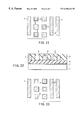
- FIG. 27 is a sectional structural diagram showing a constitution of a conventional semiconductor device.
- FIG. 1 to FIG. 10 show the manufacturing process of a semiconductor device having metal wiring, and are sectional views for explaining part of the manufacturing process of the present invention having a dummy pattern etching step.
- a MOSFET (not shown) and an element separation region 7 are formed by a known technology.
- a phosphorus-containing SiO 2 film is deposited as an interlayer insulating film 6 in 7000 angstroms by chemical vapor phase growth method, and it is further flattened by CMP technology.
- This CMP is a technology of flattening the film on the wafer while etching by a complex process of chemical reaction and mechanical polishing between the film to be polished and the abrasive.
- the apparatus consists of, as shown in FIG. 2, a head 20 sucking the wafer with the surface down, and a table 21 on which an independently rotating polishing cloth is adhered, and the head 20 is pressed against the table 21 while injecting the abrasive to polish.
- the CMP technology is applied in flattening of the interlayer insulating film, burying of multi-layer metal, or burying of poly-Si into trench, and it is used in mass production since start of manufacture of 64M DRAM.
- the abrasive and polishing cloth are different.
- abrasive particles colloidal silica, cerium oxide, aluminum oxide and the like may be used.
- the polishing cloth various types may be used, including soft and stiff materials, and flat and fluted materials.
- the end point detecting method the polishing time is calculated from the polishing rate to the film thickness to be polished, and the end point is detected.
- the CMP is cutting of wafer surface by abrasive, in principle, it is a process accompanied by generation of particles, and the wafer surface is contaminated by metal impurities and the like in the abrasive, and hence after-process cleaning is important.
- the method of cleaning what is most general is the brushing method for removing particles physically. Since several kinds of films appear on the surface after CMP, particles and metal impurities must be removed from all of them. To remove them, surface active agents and the like are added, and the removal level is considerably improved.
- a metal wiring film 11 Al—Si—Cu alloy or the like
- RIE reactive ion etching
- an SiO 2 interlayer insulating film 8 is deposited in 14000 angstroms by plasma CVD technology. Then, as shown in FIG. 6, the interlayer insulating film 8 is flattened by the CMP technology so that the metal patterns 2 , 3 of the first layer may not be exposed.
- opening holes for dummy pattern etching that is, holes 9 are opened.
- FIG. 8 by using an etching solution mixing sulfuric acid and hydrogen peroxide by 1:1, the metal pattern 3 of the first layer used as dummy pattern is selectively etched anisotropically.
- an SiO 2 interlayer insulating film 10 is deposited by 7000 angstroms again by plasma CVD technology. As a result, the holes 9 are filled with the insulating film 10 . Then, a through-hole for coupling the metal of the first layer and the metal of the second layer is formed by lithographic technology and reactive ion etching technology (not shown).
- a metal wiring film (Al—Si—Cu alloy or the like) is formed in 7000 angstroms by sputtering, and the metal wiring of the second layer is patterned by lithographic technology and reactive ion etching technology as shown in FIG. 10 . As a result, the wiring 5 used as the signal line of the metal wiring of the second layer is formed. Then, forming a passivation film by a known technology, the pad portion is selectively opened as electrode.
- the dummy pattern shape of the present invention for enhancing the flatness in the case of CMP flattening, and various examples of constitution and operation of opening holes for etching the dummy pattern are explained below by referring to FIG. 11 to FIG. 26 .
- FIG. 11A is a plan view showing an example of constitution of forming a relatively large dummy pattern as compared with the wiring pattern 2 , etching this dummy pattern through plural opening holes 9 , and forming cavities 12 .
- FIG. 11B is a plan view of fabricating up to the second layer wiring pattern 5 of the upper layer as compared with the constitution in FIG. 11 A.
- FIG. 12A shows an example of constitution of forming plural rectangular dummy patterns in the wiring pattern 2 , etching the dummy patterns through individual opening holes 9 , and forming cavities 12 .
- FIG. 12B is a plan view of fabricating up to the second layer wiring pattern 5 of the upper layer as compared with the constitution in FIG. 12 A.
- FIG. 13 is a sectional view of composing the second layer metal wiring of the upper layer in the upper part of the cavity.
- the parasitic capacity C P of the upper layer wiring includes the space portion of the cavity 12 .
- the delay of the signal transmitted through the second layer metal wiring 5 may be smaller as compared with the case in which the dummy pattern is present as metal pattern.
- FIG. 14 to FIG. 26 are diagrams for explaining part of the manufacturing process of the semiconductor device according to the present invention, by forming plural dummy patterns in metal wirings, etching these dummy patterns selectively, and forming cavities.
- an element separation region 7 and MOSFET (not shown) are formed by a known technology.
- a phosphorus-containing SiO 2 interlayer insulating film 6 is deposited in 7000 angstroms by chemical vapor phase growth method, and it is further flattened by CMP technology.
- a metal wiring film 11 (Al—Si—Cu alloy or the like) is formed in 7000 angstroms by sputtering technology.
- the metal layer of first layer is patterned by lithographic technology and reactive ion etching technology by RIE.
- the wiring 2 used as signal line and dummy pattern 3 for enhancing the flatness in flattening are formed.
- FIG. 17 shows a plan view at this time. In this way, the dummy pattern 3 for enhancing the flatness when flattening is divided into plural sections.
- an SiO 2 interlayer insulating film 8 is deposited in 14000 angstroms by plasma CVD technology.
- the SiO 2 interlayer insulating film 8 is flattened by CMP technology so that the first layer metals 2 , 3 may not be exposed.
- opening holes 9 for dummy pattern etching are formed selectively in the interlayer insulating film 8 .
- a plan view at this time is shown in FIG. 21 .
- the divided dummy patterns only those free from problem in strength when cavities are formed are opened to form holes 9 .
- FIG. 22 shows a plan view at this time.
- the arranged dummy patterns are removed so as to be free from problem in strength.
- an SiO 2 interlayer insulating film 19 is deposited in 7000 angstroms again by plasma CVD technology. As a result, the holes 9 are filled with the insulating film. Then, a through-hole for coupling the metal of the first layer and the metal of the second layer is formed by lithographic technology and reactive ion etching technology (not shown).
- an Al—Si—Cu alloy is formed in 7000 angstroms by sputtering, and the metal wiring of the second layer is patterned by lithographic technology and reactive ion etching technology as shown in FIG. 25 .
- the wiring 5 used as the signal line of the metal wiring of the second layer is formed.
- FIG. 26 is a plan view at this time. Then, a passivation film is formed by a known technology, the pad portion is selectively opened as electrode.
- the first layer metal is used in forming the dummy pattern, but SiN, poly-Si, carbon or the like may be also used.
- the dummy patterns can be formed.
- the flatness of the CMP can be enhanced by using the dummy pattern, and the parasitic capacity of the wiring can be substantially decreased.
- metal wiring of floating is not needed, and the difficult of circuit design is extremely improved.
Abstract
Dummy patterns are formed in signal patterns of a first metal layer, an insulating film covering such patterns is flattened by CMP, and only dummy patterns are selectively etched by anisotropic etching through holes opened at specific intervals. Then the opened holes are filled with an insulating film, and cavities are formed. In the upper part of the cavity, a signal line of the second metal layer is formed. As a result, a semiconductor device is provided by the CMP flattening technology without being accompanied by increase of parasitic capacity between signal lines by metal dummy patterns or shorting due to dust and the like.
Description
The present invention relates to a semiconductor device and its manufacturing method, and more particularly to a multi-layer metal wiring technology.
Hitherto, in a semiconductor device having metal wiring of two or more layers, when the lower surface of the metal wiring layer is flattened by CMP (chemical mechanical polishing) technology, a dummy pattern is generally disposed for enhancement of its flatness.
FIG. 27 is a sectional view showing a constitution for disposing two-layer metal wiring on a semiconductor device. After forming a semiconductor element, an interlayer insulating film 6, and the like on a silicon substrate 1, the metal wiring layer of first layer is patterned by lithographic technology and reactive ion etching technology. As a result, a signal line pattern 2 and a dummy pattern 3 for enhancing the flatness in the subsequent CMP process are formed.
Consequently, after depositing an SiO2 interlayer insulating film 4 by plasma CVD technology, the interlayer insulating film 4 is flattened by the CMP technology so that the metal pattern of the first layer may not be exposed. Same as in the first layer, next, the signal line pattern 5 is patterned by the lithographic technology and reactive ion etching technology. In this way, in the metal wiring layer of the first layer, a dummy pattern 3 is present besides the signal line 2 and power source wire actually used as wiring.
In such conventional constitution, by placing the dummy pattern for enhancing the flatness in CMP flattening process, a problem of increase of parasitic capacity between signal lines occurs. As the parasitic capacity between signal lines increases, not only the signal propagation speed is lowered, but also the noise resistance of the device drops. Besides, owing to the dummy pattern, the resistance to dust becomes weaker, and the signal lines are shorted, and probability of lowering of yield becomes higher. Still worse, since the dummy pattern is in an electrically floating state, simulation by circuit simulator is difficult, and the circuit design is very difficult.
The present invention is devised to solve the aforementioned problems, and it is hence an object thereof to provide a semiconductor device manufactured by CMP flattening process not accompanied by increase of parasitic capacity between signal lines due to metal dummy pattern used for CMP flattening, shorting due to dust and the like, or complication of circuit design, and a method of manufacturing the same.
To achieve the aforementioned object, according to the present invention, after completion of flattening by CMP, a dummy pattern is selectively etched by anisotropic etching through holes opened at specific intervals, and the opened holes are filled with an insulating film, and a cavity is formed. By forming a cavity in the portion of the dummy pattern in this manner, it is intended to solve the problem of parasitic capacity and difficulty of circuit design.
That is, the semiconductor device of the present invention comprises wiring patterns and dummy patterns formed on a first insulating film, a second insulating film provided in a region on the first insulating film containing the wiring patterns and dummy patterns, having the surface flattened by CMP, and second wiring patterns disposed on the second insulating film, in which the dummy patterns are formed selectively in cavities.
A semiconductor device manufacturing method of the present invention comprises a step of forming plural wiring patterns and plural dummy patterns on the first insulating film, a step of depositing a second insulating film in a region on the first insulating film including the plural wiring patterns and dummy patterns, a step of flattening the surface of the second insulating film by using the CMP technology, a step of selectively providing opening holes in the second insulating film on the plural dummy patterns, a step of etching the dummy patterns through the opening holes, a step of depositing a third insulating film in a region on the second insulating film including the opening holes, and a step of forming second wiring patterns on the third insulating film.
Since the dummy patterns are selectively etched by the anisotropic etching after completion of flattening by CMP, cavities are formed in the dummy patterns. As a result, the parasitic capacity between the signal lines decreases, and complication of circuit design can be prevented.
Additional objects and advantages of the invention will be set forth in the description which follows, and in part will be obvious from the description, or may be learned by practice of the invention. The objects and advantages of the invention may be realized and obtained by means of the instrumentalities and combinations particularly pointed out hereinafter.
The accompanying drawings, which are incorporated in and constitute a part of the specification, illustrate presently preferred embodiments of the invention, and together with the general description given above and the detailed description of the preferred embodiments given below, serve to explain the principles of the invention.
FIG. 1 is a sectional structural diagram for explaining a manufacturing process of a semiconductor device of the present invention;
FIG. 2 is a perspective view for explaining a CMP technology;
FIG. 3 is a sectional structural diagram for explaining a manufacturing process of a semiconductor device of the present invention;
FIG. 4 is a sectional structural diagram for explaining a manufacturing process of a semiconductor device of the present invention;
FIG. 5 is a sectional structural diagram for explaining a manufacturing process of a semiconductor device of the present invention;
FIG. 6 is a sectional structural diagram for explaining a manufacturing process of a semiconductor device of the present invention;
FIG. 7 is a sectional structural diagram for explaining a manufacturing process of a semiconductor device of the present invention;
FIG. 8 is a sectional structural diagram for explaining a manufacturing process of a semiconductor device of the present invention;
FIG. 9 is a sectional structural diagram for explaining a manufacturing process of a semiconductor device of the present invention;
FIG. 10 is a sectional structural diagram for explaining a manufacturing process of a semiconductor device of the present invention;
FIGS. 11A and 11B are plan views showing a constitution of a semiconductor device of the present invention;
FIGS. 12A and 12B are plan views showing a constitution of a semiconductor device of the present invention;
FIG. 13 is a sectional view for explaining the operation of a semiconductor device of the present invention;
FIG. 14 is a sectional structural diagram for explaining a manufacturing process of a semiconductor device of the present invention;
FIG. 15 is a sectional structural diagram for explaining a manufacturing process of a semiconductor device of the present invention;
FIG. 16 is a sectional structural diagram for explaining a manufacturing process of a semiconductor device of the present invention;
FIG. 17 is a plan view for explaining a manufacturing process of a semiconductor device of the present invention;
FIG. 18 is a sectional structural diagram for explaining a manufacturing process of a semiconductor device of the present invention;
FIG. 19 is a sectional structural diagram for explaining a manufacturing process of a semiconductor device of the present invention;
FIG. 20 is a sectional structural diagram for explaining a manufacturing process of a semiconductor device of the present invention;
FIG. 21 is a plan view for explaining a manufacturing process of a semiconductor device of the present invention;
FIG. 22 is a sectional structural diagram for explaining a manufacturing process of a semiconductor device of the present invention;
FIG. 23 is a plan view for explaining a manufacturing process of a semiconductor device of the present invention;
FIG. 24 is a sectional structural diagram for explaining a manufacturing process of a semiconductor device of the present invention;
FIG. 25 is a sectional structural diagram for explaining a manufacturing process of a semiconductor device of the present invention;
FIG. 26 is a plan view for explaining a manufacturing process of a semiconductor device of the present invention; and
FIG. 27 is a sectional structural diagram showing a constitution of a conventional semiconductor device.
Referring to the drawings, preferred embodiments of the present invention are described in detail below.
FIG. 1 to FIG. 10 show the manufacturing process of a semiconductor device having metal wiring, and are sectional views for explaining part of the manufacturing process of the present invention having a dummy pattern etching step.
First, as shown in FIG. 1, on a P-type silicon single crystal substrate 1, for example, a MOSFET (not shown) and an element separation region 7 are formed by a known technology. Then, a phosphorus-containing SiO2 film is deposited as an interlayer insulating film 6 in 7000 angstroms by chemical vapor phase growth method, and it is further flattened by CMP technology.
This CMP is a technology of flattening the film on the wafer while etching by a complex process of chemical reaction and mechanical polishing between the film to be polished and the abrasive. The apparatus consists of, as shown in FIG. 2, a head 20 sucking the wafer with the surface down, and a table 21 on which an independently rotating polishing cloth is adhered, and the head 20 is pressed against the table 21 while injecting the abrasive to polish.
The CMP technology is applied in flattening of the interlayer insulating film, burying of multi-layer metal, or burying of poly-Si into trench, and it is used in mass production since start of manufacture of 64M DRAM. When the film to be polished varies, aside from the polishing condition (applied load, table rotating number and the like), the abrasive and polishing cloth are different. As abrasive particles, colloidal silica, cerium oxide, aluminum oxide and the like may be used. As the polishing cloth, various types may be used, including soft and stiff materials, and flat and fluted materials.
In application of CMP in device manufacturing process, what is important is the method of detecting the end point to determine when to stop polishing, and the method of cleaning after CMP process. As the end point detecting method, the polishing time is calculated from the polishing rate to the film thickness to be polished, and the end point is detected. Besides, since the CMP is cutting of wafer surface by abrasive, in principle, it is a process accompanied by generation of particles, and the wafer surface is contaminated by metal impurities and the like in the abrasive, and hence after-process cleaning is important. As the method of cleaning, what is most general is the brushing method for removing particles physically. Since several kinds of films appear on the surface after CMP, particles and metal impurities must be removed from all of them. To remove them, surface active agents and the like are added, and the removal level is considerably improved.
After such flattening by CMP, as shown in FIG. 3, a metal wiring film 11 (Al—Si—Cu alloy or the like) is formed in a thickness of 7000 angstroms by sputtering. Consequently, as shown in FIG. 4, the metal wiring of the first layer is patterned by lithographic technology and reactive ion etching (RIE) technology. As a result, the wiring 2 used as signal line and dummy pattern 3 for enhancing the flatness in CMP flattening are formed.
Consequently, as shown in FIG. 5, an SiO2 interlayer insulating film 8 is deposited in 14000 angstroms by plasma CVD technology. Then, as shown in FIG. 6, the interlayer insulating film 8 is flattened by the CMP technology so that the metal patterns 2, 3 of the first layer may not be exposed.
Next, as shown in FIG. 7, by the lithographic technology and reactive ion etching technology in the condition for selectively etching the interlayer insulating film 8, opening holes for dummy pattern etching, that is, holes 9 are opened. In succession, as shown in FIG. 8, by using an etching solution mixing sulfuric acid and hydrogen peroxide by 1:1, the metal pattern 3 of the first layer used as dummy pattern is selectively etched anisotropically.
As shown in FIG. 9, sequentially, in order to plug the holes 9 opened for dummy pattern etching, an SiO2 interlayer insulating film 10 is deposited by 7000 angstroms again by plasma CVD technology. As a result, the holes 9 are filled with the insulating film 10. Then, a through-hole for coupling the metal of the first layer and the metal of the second layer is formed by lithographic technology and reactive ion etching technology (not shown).
As the metal wiring film of the second layer, a metal wiring film (Al—Si—Cu alloy or the like) is formed in 7000 angstroms by sputtering, and the metal wiring of the second layer is patterned by lithographic technology and reactive ion etching technology as shown in FIG. 10. As a result, the wiring 5 used as the signal line of the metal wiring of the second layer is formed. Then, forming a passivation film by a known technology, the pad portion is selectively opened as electrode.
The dummy pattern shape of the present invention for enhancing the flatness in the case of CMP flattening, and various examples of constitution and operation of opening holes for etching the dummy pattern are explained below by referring to FIG. 11 to FIG. 26.
FIG. 11A is a plan view showing an example of constitution of forming a relatively large dummy pattern as compared with the wiring pattern 2, etching this dummy pattern through plural opening holes 9, and forming cavities 12. FIG. 11B is a plan view of fabricating up to the second layer wiring pattern 5 of the upper layer as compared with the constitution in FIG. 11A.
FIG. 12A shows an example of constitution of forming plural rectangular dummy patterns in the wiring pattern 2, etching the dummy patterns through individual opening holes 9, and forming cavities 12. FIG. 12B is a plan view of fabricating up to the second layer wiring pattern 5 of the upper layer as compared with the constitution in FIG. 12A.
FIG. 13 is a sectional view of composing the second layer metal wiring of the upper layer in the upper part of the cavity. As shown in the diagram, when the second layer metal wiring 5 is formed on the cavity 12, the parasitic capacity CP of the upper layer wiring includes the space portion of the cavity 12. As a result, the delay of the signal transmitted through the second layer metal wiring 5 may be smaller as compared with the case in which the dummy pattern is present as metal pattern.
FIG. 14 to FIG. 26 are diagrams for explaining part of the manufacturing process of the semiconductor device according to the present invention, by forming plural dummy patterns in metal wirings, etching these dummy patterns selectively, and forming cavities.
First, as shown in FIG. 14, on a P-type silicon single crystal substrate 1, for example, an element separation region 7 and MOSFET (not shown) are formed by a known technology. Then, a phosphorus-containing SiO2 interlayer insulating film 6 is deposited in 7000 angstroms by chemical vapor phase growth method, and it is further flattened by CMP technology.
Next, as shown in FIG. 15, a metal wiring film 11 (Al—Si—Cu alloy or the like) is formed in 7000 angstroms by sputtering technology.
As shown in FIG. 16, consequently, the metal layer of first layer is patterned by lithographic technology and reactive ion etching technology by RIE. As a result, the wiring 2 used as signal line and dummy pattern 3 for enhancing the flatness in flattening are formed. FIG. 17 shows a plan view at this time. In this way, the dummy pattern 3 for enhancing the flatness when flattening is divided into plural sections.
Then, as shown in FIG. 18, an SiO2 interlayer insulating film 8 is deposited in 14000 angstroms by plasma CVD technology. Next, as shown in FIG. 19, the SiO2 interlayer insulating film 8 is flattened by CMP technology so that the first layer metals 2, 3 may not be exposed.
Consequently, as shown in FIG. 20, by lithographic technology, opening holes 9 for dummy pattern etching are formed selectively in the interlayer insulating film 8. A plan view at this time is shown in FIG. 21. Of the divided dummy patterns, only those free from problem in strength when cavities are formed are opened to form holes 9.
As shown in FIG. 22, by a chemical solution mixing sulfuric acid and hydrogen peroxide, the first layer metal pattern used as dummy pattern is selectively removed. FIG. 23 shows a plan view at this time. The arranged dummy patterns are removed so as to be free from problem in strength.
Next, as shown in FIG. 24, to plug the holes 9 opened for removing the dummy pattern, an SiO2 interlayer insulating film 19 is deposited in 7000 angstroms again by plasma CVD technology. As a result, the holes 9 are filled with the insulating film. Then, a through-hole for coupling the metal of the first layer and the metal of the second layer is formed by lithographic technology and reactive ion etching technology (not shown).
As the metal wiring film of the second layer, an Al—Si—Cu alloy is formed in 7000 angstroms by sputtering, and the metal wiring of the second layer is patterned by lithographic technology and reactive ion etching technology as shown in FIG. 25. As a result, the wiring 5 used as the signal line of the metal wiring of the second layer is formed. FIG. 26 is a plan view at this time. Then, a passivation film is formed by a known technology, the pad portion is selectively opened as electrode.
In the description of the foregoing embodiments, the first layer metal is used in forming the dummy pattern, but SiN, poly-Si, carbon or the like may be also used. When such material is used, by forming films of such materials after forming the metal wiring of the first layer, and patterning the films by lithographic technology, the dummy patterns can be formed.
As described herein, according to the present invention, the flatness of the CMP can be enhanced by using the dummy pattern, and the parasitic capacity of the wiring can be substantially decreased. In the circuit design, moreover, metal wiring of floating is not needed, and the difficult of circuit design is extremely improved.
Additional advantages and modifications will readily occur to those skilled in the art. Therefore, the invention in its broader aspects is not limited to the specific details and representative embodiments shown and described herein. Accordingly, various modifications may be made without departing from the spirit or scope of the general inventive concept as defined by the appended claims and their equivalents.
Claims (5)
1. A semiconductor device comprising:
first wiring patterns formed on the first insulating film and extending in a first direction;
a second insulating film formed on the first insulating film and the first wirings;
a plurality of cavities and at least one dummy pattern formed in the second insulating film and which are formed between the first wiring patterns and have the same height as the first wiring patterns, regions between the cavities and the first wiring patterns being filled with the second insulating film; and
a second wiring formed above the second insulating film and extending in the first direction, the second wiring being located above the cavities.
2. A new semiconductor device according to claim 1 , further comprising a third insulating film formed on the second insulating film, and wherein said second wiring is formed on the third insulating film.
3. A semiconductor device according to claim 1 , wherein at least part of said second wiring is located right above at least one of the cavities.
4. A semiconductor device according to claim 1 , wherein the plurality of cavities are arranged in the first direction.
5. A semiconductor device according to claim 1 , further comprising a plurality of dummy patterns arranged in the first direction between the first wiring patterns.
Applications Claiming Priority (2)
| Application Number | Priority Date | Filing Date | Title |
|---|---|---|---|
| JP9-319709 | 1997-11-20 | ||
| JP9319709A JPH11154675A (en) | 1997-11-20 | 1997-11-20 | Semiconductor device and manufacture thereof |
Publications (2)
| Publication Number | Publication Date |
|---|---|
| US20020000663A1 US20020000663A1 (en) | 2002-01-03 |
| US6396146B2 true US6396146B2 (en) | 2002-05-28 |
Family
ID=18113312
Family Applications (1)
| Application Number | Title | Priority Date | Filing Date |
|---|---|---|---|
| US09/195,614 Expired - Fee Related US6396146B2 (en) | 1997-11-20 | 1998-11-19 | Semiconductor device and its manufacturing method |
Country Status (2)
| Country | Link |
|---|---|
| US (1) | US6396146B2 (en) |
| JP (1) | JPH11154675A (en) |
Cited By (7)
| Publication number | Priority date | Publication date | Assignee | Title |
|---|---|---|---|---|
| US20030146495A1 (en) * | 2000-07-13 | 2003-08-07 | Matsushita Electric Industrial Co., Ltd. | Semiconductor device and method for fabricating the same |
| US6693357B1 (en) | 2003-03-13 | 2004-02-17 | Texas Instruments Incorporated | Methods and semiconductor devices with wiring layer fill structures to improve planarization uniformity |
| US20040084749A1 (en) * | 2001-03-01 | 2004-05-06 | Werner Pamler | Hollow structure in an integrated circuit and method for producing such a hollow structure in an integrated circuit |
| US6951806B1 (en) * | 1999-11-30 | 2005-10-04 | Sun Microsystems, Inc. | Metal region for reduction of capacitive coupling between signal lines |
| US20050287779A1 (en) * | 2004-06-25 | 2005-12-29 | Chuan-Yi Lin | Integrated circuit structure and method of fabrication |
| US20070184646A1 (en) * | 2002-12-10 | 2007-08-09 | Fujitsu Limited | Semiconductor device, wiring substrate forming method, and substrate processing apparatus |
| US20090170323A1 (en) * | 2007-12-27 | 2009-07-02 | Masanori Miyata | Chemical mechanical polishing method and chemical mechanical polishing device |
Families Citing this family (7)
| Publication number | Priority date | Publication date | Assignee | Title |
|---|---|---|---|---|
| US6943447B2 (en) | 2002-01-10 | 2005-09-13 | Fujitsu Limited | Thin film multi-layer wiring substrate having a coaxial wiring structure in at least one layer |
| FR2844096A1 (en) * | 2002-08-30 | 2004-03-05 | St Microelectronics Sa | METHOD FOR MANUFACTURING AN ELECTRICAL CIRCUIT COMPRISING A POLISHING STEP |
| DE10348641A1 (en) * | 2003-10-15 | 2005-05-25 | Infineon Technologies Ag | Method for reducing parasitic couplings in circuits |
| JP4671614B2 (en) * | 2004-03-03 | 2011-04-20 | パナソニック株式会社 | Semiconductor device |
| JP2011233807A (en) * | 2010-04-30 | 2011-11-17 | Panasonic Corp | Semiconductor device and manufacturing method therefor |
| WO2017064937A1 (en) * | 2015-10-16 | 2017-04-20 | ソニー株式会社 | Semiconductor device and method for manufacturing semiconductor device |
| US10096522B2 (en) * | 2016-05-06 | 2018-10-09 | Taiwan Semiconductor Manufacturing Co., Ltd. | Dummy MOL removal for performance enhancement |
Citations (8)
| Publication number | Priority date | Publication date | Assignee | Title |
|---|---|---|---|---|
| JPS63211739A (en) * | 1987-02-27 | 1988-09-02 | Nec Corp | Semiconductor device |
| US5461003A (en) * | 1994-05-27 | 1995-10-24 | Texas Instruments Incorporated | Multilevel interconnect structure with air gaps formed between metal leads |
| US5519250A (en) * | 1994-05-31 | 1996-05-21 | Numata; Ken | Reliability of metal leads in high speed LSI semiconductors using both dummy leads and thermoconductive layers |
| JPH10189509A (en) | 1996-12-26 | 1998-07-21 | Toshiba Corp | Semiconductor device and its manufacturing method |
| US5792706A (en) * | 1996-06-05 | 1998-08-11 | Advanced Micro Devices, Inc. | Interlevel dielectric with air gaps to reduce permitivity |
| US5835987A (en) * | 1995-10-31 | 1998-11-10 | Micron Technology, Inc. | Reduced RC delay between adjacent substrate wiring lines |
| US5861674A (en) * | 1997-02-20 | 1999-01-19 | Nec Corporation | Multilevel interconnection in a semiconductor device and method for forming the same |
| US5863832A (en) * | 1996-06-28 | 1999-01-26 | Intel Corporation | Capping layer in interconnect system and method for bonding the capping layer onto the interconnect system |
-
1997
- 1997-11-20 JP JP9319709A patent/JPH11154675A/en active Pending
-
1998
- 1998-11-19 US US09/195,614 patent/US6396146B2/en not_active Expired - Fee Related
Patent Citations (9)
| Publication number | Priority date | Publication date | Assignee | Title |
|---|---|---|---|---|
| JPS63211739A (en) * | 1987-02-27 | 1988-09-02 | Nec Corp | Semiconductor device |
| US5461003A (en) * | 1994-05-27 | 1995-10-24 | Texas Instruments Incorporated | Multilevel interconnect structure with air gaps formed between metal leads |
| US5519250A (en) * | 1994-05-31 | 1996-05-21 | Numata; Ken | Reliability of metal leads in high speed LSI semiconductors using both dummy leads and thermoconductive layers |
| US5835987A (en) * | 1995-10-31 | 1998-11-10 | Micron Technology, Inc. | Reduced RC delay between adjacent substrate wiring lines |
| US5792706A (en) * | 1996-06-05 | 1998-08-11 | Advanced Micro Devices, Inc. | Interlevel dielectric with air gaps to reduce permitivity |
| US5863832A (en) * | 1996-06-28 | 1999-01-26 | Intel Corporation | Capping layer in interconnect system and method for bonding the capping layer onto the interconnect system |
| JPH10189509A (en) | 1996-12-26 | 1998-07-21 | Toshiba Corp | Semiconductor device and its manufacturing method |
| US6091130A (en) | 1996-12-26 | 2000-07-18 | Kabushiki Kaisha Toshiba | Semiconductor device having structure suitable for CMP process |
| US5861674A (en) * | 1997-02-20 | 1999-01-19 | Nec Corporation | Multilevel interconnection in a semiconductor device and method for forming the same |
Cited By (15)
| Publication number | Priority date | Publication date | Assignee | Title |
|---|---|---|---|---|
| US6951806B1 (en) * | 1999-11-30 | 2005-10-04 | Sun Microsystems, Inc. | Metal region for reduction of capacitive coupling between signal lines |
| US20030146495A1 (en) * | 2000-07-13 | 2003-08-07 | Matsushita Electric Industrial Co., Ltd. | Semiconductor device and method for fabricating the same |
| US7233052B2 (en) | 2000-07-13 | 2007-06-19 | Matsushita Electric Industrial Co., Ltd. | Semiconductor device including fine dummy patterns |
| US6890830B2 (en) | 2000-07-13 | 2005-05-10 | Matsushita Electric Industrial Co., Ltd. | Semiconductor device and method for fabricating the same |
| US20050161824A1 (en) * | 2000-07-13 | 2005-07-28 | Matsushita Electric Industrial Co., Ltd. | Semiconductor device and method for fabricating the same |
| US7259441B2 (en) * | 2001-03-01 | 2007-08-21 | Infineon Technologies Ag | Hollow structure in an integrated circuit and method for producing such a hollow structure in an integrated circuit |
| US20040084749A1 (en) * | 2001-03-01 | 2004-05-06 | Werner Pamler | Hollow structure in an integrated circuit and method for producing such a hollow structure in an integrated circuit |
| US20070184646A1 (en) * | 2002-12-10 | 2007-08-09 | Fujitsu Limited | Semiconductor device, wiring substrate forming method, and substrate processing apparatus |
| US7648907B2 (en) | 2002-12-10 | 2010-01-19 | Fujitsu Limited | Semiconductor device, wiring substrate forming method, and substrate processing apparatus |
| US7704856B2 (en) | 2002-12-10 | 2010-04-27 | Fujitsu Limited | Semiconductor device, wiring substrate forming method, and substrate processing apparatus |
| US6693357B1 (en) | 2003-03-13 | 2004-02-17 | Texas Instruments Incorporated | Methods and semiconductor devices with wiring layer fill structures to improve planarization uniformity |
| US20050287779A1 (en) * | 2004-06-25 | 2005-12-29 | Chuan-Yi Lin | Integrated circuit structure and method of fabrication |
| US7271431B2 (en) | 2004-06-25 | 2007-09-18 | Taiwan Semiconductor Manufacturing Company, Ltd. | Integrated circuit structure and method of fabrication |
| US20090170323A1 (en) * | 2007-12-27 | 2009-07-02 | Masanori Miyata | Chemical mechanical polishing method and chemical mechanical polishing device |
| US8116894B2 (en) * | 2007-12-27 | 2012-02-14 | Ricoh Company, Ltd. | Chemical mechanical polishing method and chemical mechanical polishing device |
Also Published As
| Publication number | Publication date |
|---|---|
| US20020000663A1 (en) | 2002-01-03 |
| JPH11154675A (en) | 1999-06-08 |
Similar Documents
| Publication | Publication Date | Title |
|---|---|---|
| US6831367B2 (en) | Semiconductor device and method of manufacturing the same | |
| EP0284840B1 (en) | Method for forming uniform layers of material | |
| KR100272499B1 (en) | Method for forming self aligned vias in multi level metal integrated circuit | |
| US5071792A (en) | Process for forming extremely thin integrated circuit dice | |
| US5246883A (en) | Semiconductor contact via structure and method | |
| US6396146B2 (en) | Semiconductor device and its manufacturing method | |
| US5619072A (en) | High density multi-level metallization and interconnection structure | |
| JP3360350B2 (en) | Surface flattening method | |
| KR100268210B1 (en) | Process for reducing pattern factor effects in cmp planarization | |
| JPH0745616A (en) | Manufacture of semiconductor device | |
| CN112509915B (en) | Semiconductor device, manufacturing method thereof and chip bonding structure | |
| JP3163719B2 (en) | Method for manufacturing semiconductor device having polishing step | |
| CN109994444B (en) | Wafer bonding structure and manufacturing method thereof | |
| US6864177B2 (en) | Method for manufacturing metal line contact plug of semiconductor device | |
| JPH04229625A (en) | Manufacture of semiconductor device | |
| JPH11150116A (en) | Method for forming contact plug of semiconductor device | |
| US6114232A (en) | Method for making an electrical contact to a node location and process for forming a conductive line or other circuit component | |
| JP2002299433A (en) | Method of forming element separating film of semiconductor element | |
| JPH10335459A (en) | Semiconductor device and its manufacture | |
| US5948698A (en) | Manufacturing method of semiconductor device using chemical mechanical polishing | |
| US6723644B2 (en) | Method of fabricating a semiconductor device using two chemical mechanical polishing processes to polish regions having different conductive pattern densities | |
| US20020084530A1 (en) | Conductive lines with reduced pitch | |
| EP0878836A2 (en) | Planarising a semiconductor substrate | |
| US5633207A (en) | Method of forming a wiring layer for a semiconductor device | |
| US7074702B2 (en) | Methods of manufacturing semiconductor devices |
Legal Events
| Date | Code | Title | Description |
|---|---|---|---|
| AS | Assignment |
Owner name: KABUSHIKI KAISHA TOSHIBA, JAPAN Free format text: ASSIGNMENT OF ASSIGNORS INTEREST;ASSIGNOR:NAKAYAMA, TAKEO;REEL/FRAME:009568/0163 Effective date: 19981113 |
|
| FPAY | Fee payment |
Year of fee payment: 4 |
|
| REMI | Maintenance fee reminder mailed | ||
| LAPS | Lapse for failure to pay maintenance fees | ||
| STCH | Information on status: patent discontinuation |
Free format text: PATENT EXPIRED DUE TO NONPAYMENT OF MAINTENANCE FEES UNDER 37 CFR 1.362 |
|
| FP | Expired due to failure to pay maintenance fee |
Effective date: 20100528 |