US6387761B1 - Anneal for enhancing the electrical characteristic of semiconductor devices - Google Patents
Anneal for enhancing the electrical characteristic of semiconductor devices Download PDFInfo
- Publication number
- US6387761B1 US6387761B1 US09/499,336 US49933600A US6387761B1 US 6387761 B1 US6387761 B1 US 6387761B1 US 49933600 A US49933600 A US 49933600A US 6387761 B1 US6387761 B1 US 6387761B1
- Authority
- US
- United States
- Prior art keywords
- silicon nitride
- substrate
- ambient
- forming
- silicon
- Prior art date
- Legal status (The legal status is an assumption and is not a legal conclusion. Google has not performed a legal analysis and makes no representation as to the accuracy of the status listed.)
- Expired - Fee Related
Links
- 239000004065 semiconductor Substances 0.000 title claims description 14
- 230000002708 enhancing effect Effects 0.000 title description 3
- HQVNEWCFYHHQES-UHFFFAOYSA-N silicon nitride Chemical compound N12[Si]34N5[Si]62N3[Si]51N64 HQVNEWCFYHHQES-UHFFFAOYSA-N 0.000 claims abstract description 83
- 229910052581 Si3N4 Inorganic materials 0.000 claims abstract description 68
- 239000000758 substrate Substances 0.000 claims abstract description 60
- 238000000034 method Methods 0.000 claims abstract description 33
- XUIMIQQOPSSXEZ-UHFFFAOYSA-N Silicon Chemical compound [Si] XUIMIQQOPSSXEZ-UHFFFAOYSA-N 0.000 claims abstract description 22
- 229910052710 silicon Inorganic materials 0.000 claims abstract description 22
- 239000010703 silicon Substances 0.000 claims abstract description 22
- 239000001257 hydrogen Substances 0.000 claims abstract description 9
- 229910052739 hydrogen Inorganic materials 0.000 claims abstract description 9
- 229910021420 polycrystalline silicon Inorganic materials 0.000 claims description 18
- 229920005591 polysilicon Polymers 0.000 claims description 18
- 238000000137 annealing Methods 0.000 claims description 13
- IJGRMHOSHXDMSA-UHFFFAOYSA-N Atomic nitrogen Chemical compound N#N IJGRMHOSHXDMSA-UHFFFAOYSA-N 0.000 claims description 7
- 238000010438 heat treatment Methods 0.000 claims description 7
- 150000002431 hydrogen Chemical class 0.000 claims description 6
- UFHFLCQGNIYNRP-UHFFFAOYSA-N Hydrogen Chemical compound [H][H] UFHFLCQGNIYNRP-UHFFFAOYSA-N 0.000 claims description 5
- 229910052751 metal Inorganic materials 0.000 claims description 5
- 239000002184 metal Substances 0.000 claims description 5
- 229910021421 monocrystalline silicon Inorganic materials 0.000 claims description 5
- 229910000314 transition metal oxide Inorganic materials 0.000 claims description 5
- 229910052757 nitrogen Inorganic materials 0.000 claims 1
- 125000004435 hydrogen atom Chemical class [H]* 0.000 abstract 1
- 239000010410 layer Substances 0.000 description 44
- 239000007789 gas Substances 0.000 description 36
- 239000003990 capacitor Substances 0.000 description 32
- BPUBBGLMJRNUCC-UHFFFAOYSA-N oxygen(2-);tantalum(5+) Chemical compound [O-2].[O-2].[O-2].[O-2].[O-2].[Ta+5].[Ta+5] BPUBBGLMJRNUCC-UHFFFAOYSA-N 0.000 description 23
- 230000004888 barrier function Effects 0.000 description 18
- VYPSYNLAJGMNEJ-UHFFFAOYSA-N Silicium dioxide Chemical compound O=[Si]=O VYPSYNLAJGMNEJ-UHFFFAOYSA-N 0.000 description 17
- 238000000151 deposition Methods 0.000 description 14
- QVGXLLKOCUKJST-UHFFFAOYSA-N atomic oxygen Chemical compound [O] QVGXLLKOCUKJST-UHFFFAOYSA-N 0.000 description 12
- 230000008021 deposition Effects 0.000 description 12
- 239000001301 oxygen Substances 0.000 description 12
- 229910052760 oxygen Inorganic materials 0.000 description 12
- 238000004519 manufacturing process Methods 0.000 description 11
- 230000015572 biosynthetic process Effects 0.000 description 10
- 230000007547 defect Effects 0.000 description 8
- 230000008569 process Effects 0.000 description 8
- 235000012239 silicon dioxide Nutrition 0.000 description 7
- 239000000377 silicon dioxide Substances 0.000 description 7
- QGZKDVFQNNGYKY-UHFFFAOYSA-N Ammonia Chemical compound N QGZKDVFQNNGYKY-UHFFFAOYSA-N 0.000 description 6
- 238000005229 chemical vapour deposition Methods 0.000 description 5
- 230000003647 oxidation Effects 0.000 description 5
- 238000007254 oxidation reaction Methods 0.000 description 5
- 239000000463 material Substances 0.000 description 4
- GWEVSGVZZGPLCZ-UHFFFAOYSA-N Titan oxide Chemical compound O=[Ti]=O GWEVSGVZZGPLCZ-UHFFFAOYSA-N 0.000 description 3
- 238000009792 diffusion process Methods 0.000 description 3
- 229910001873 dinitrogen Inorganic materials 0.000 description 3
- 238000005530 etching Methods 0.000 description 3
- 229910000069 nitrogen hydride Inorganic materials 0.000 description 3
- 238000000206 photolithography Methods 0.000 description 3
- 229910052814 silicon oxide Inorganic materials 0.000 description 3
- XKRFYHLGVUSROY-UHFFFAOYSA-N Argon Chemical compound [Ar] XKRFYHLGVUSROY-UHFFFAOYSA-N 0.000 description 2
- BLRPTPMANUNPDV-UHFFFAOYSA-N Silane Chemical compound [SiH4] BLRPTPMANUNPDV-UHFFFAOYSA-N 0.000 description 2
- RTAQQCXQSZGOHL-UHFFFAOYSA-N Titanium Chemical compound [Ti] RTAQQCXQSZGOHL-UHFFFAOYSA-N 0.000 description 2
- 229910052454 barium strontium titanate Inorganic materials 0.000 description 2
- 239000002131 composite material Substances 0.000 description 2
- 239000003989 dielectric material Substances 0.000 description 2
- 229910052734 helium Inorganic materials 0.000 description 2
- 239000011229 interlayer Substances 0.000 description 2
- 239000007788 liquid Substances 0.000 description 2
- 238000004518 low pressure chemical vapour deposition Methods 0.000 description 2
- 125000004430 oxygen atom Chemical group O* 0.000 description 2
- 230000009467 reduction Effects 0.000 description 2
- OGIDPMRJRNCKJF-UHFFFAOYSA-N titanium oxide Inorganic materials [Ti]=O OGIDPMRJRNCKJF-UHFFFAOYSA-N 0.000 description 2
- BOTDANWDWHJENH-UHFFFAOYSA-N Tetraethyl orthosilicate Chemical compound CCO[Si](OCC)(OCC)OCC BOTDANWDWHJENH-UHFFFAOYSA-N 0.000 description 1
- ATJFFYVFTNAWJD-UHFFFAOYSA-N Tin Chemical compound [Sn] ATJFFYVFTNAWJD-UHFFFAOYSA-N 0.000 description 1
- NRTOMJZYCJJWKI-UHFFFAOYSA-N Titanium nitride Chemical compound [Ti]#N NRTOMJZYCJJWKI-UHFFFAOYSA-N 0.000 description 1
- 229910021529 ammonia Inorganic materials 0.000 description 1
- 125000000129 anionic group Chemical group 0.000 description 1
- 229910052786 argon Inorganic materials 0.000 description 1
- 125000004429 atom Chemical group 0.000 description 1
- -1 but not limited to Chemical compound 0.000 description 1
- 239000012159 carrier gas Substances 0.000 description 1
- 239000000919 ceramic Substances 0.000 description 1
- 239000007772 electrode material Substances 0.000 description 1
- 239000001307 helium Substances 0.000 description 1
- SWQJXJOGLNCZEY-UHFFFAOYSA-N helium atom Chemical compound [He] SWQJXJOGLNCZEY-UHFFFAOYSA-N 0.000 description 1
- 238000002347 injection Methods 0.000 description 1
- 239000007924 injection Substances 0.000 description 1
- 239000012212 insulator Substances 0.000 description 1
- 238000005468 ion implantation Methods 0.000 description 1
- 230000015654 memory Effects 0.000 description 1
- 229910044991 metal oxide Inorganic materials 0.000 description 1
- 150000004706 metal oxides Chemical class 0.000 description 1
- 239000000203 mixture Substances 0.000 description 1
- 150000004767 nitrides Chemical class 0.000 description 1
- 125000004433 nitrogen atom Chemical group N* 0.000 description 1
- 238000012856 packing Methods 0.000 description 1
- 238000000059 patterning Methods 0.000 description 1
- 230000035515 penetration Effects 0.000 description 1
- 239000002243 precursor Substances 0.000 description 1
- 230000002265 prevention Effects 0.000 description 1
- 229910000077 silane Inorganic materials 0.000 description 1
- 239000007787 solid Substances 0.000 description 1
- 238000003860 storage Methods 0.000 description 1
- 229910052715 tantalum Inorganic materials 0.000 description 1
- GUVRBAGPIYLISA-UHFFFAOYSA-N tantalum atom Chemical compound [Ta] GUVRBAGPIYLISA-UHFFFAOYSA-N 0.000 description 1
- 238000002230 thermal chemical vapour deposition Methods 0.000 description 1
- 238000005979 thermal decomposition reaction Methods 0.000 description 1
- 229910052719 titanium Inorganic materials 0.000 description 1
- 239000010936 titanium Substances 0.000 description 1
Images


Classifications
-
- H—ELECTRICITY
- H01—ELECTRIC ELEMENTS
- H01L—SEMICONDUCTOR DEVICES NOT COVERED BY CLASS H10
- H01L21/00—Processes or apparatus adapted for the manufacture or treatment of semiconductor or solid state devices or of parts thereof
- H01L21/02—Manufacture or treatment of semiconductor devices or of parts thereof
- H01L21/04—Manufacture or treatment of semiconductor devices or of parts thereof the devices having at least one potential-jump barrier or surface barrier, e.g. PN junction, depletion layer or carrier concentration layer
- H01L21/18—Manufacture or treatment of semiconductor devices or of parts thereof the devices having at least one potential-jump barrier or surface barrier, e.g. PN junction, depletion layer or carrier concentration layer the devices having semiconductor bodies comprising elements of Group IV of the Periodic System or AIIIBV compounds with or without impurities, e.g. doping materials
- H01L21/28—Manufacture of electrodes on semiconductor bodies using processes or apparatus not provided for in groups H01L21/20 - H01L21/268
- H01L21/28008—Making conductor-insulator-semiconductor electrodes
- H01L21/28017—Making conductor-insulator-semiconductor electrodes the insulator being formed after the semiconductor body, the semiconductor being silicon
- H01L21/28158—Making the insulator
- H01L21/28167—Making the insulator on single crystalline silicon, e.g. using a liquid, i.e. chemical oxidation
- H01L21/28185—Making the insulator on single crystalline silicon, e.g. using a liquid, i.e. chemical oxidation with a treatment, e.g. annealing, after the formation of the gate insulator and before the formation of the definitive gate conductor
-
- H—ELECTRICITY
- H01—ELECTRIC ELEMENTS
- H01L—SEMICONDUCTOR DEVICES NOT COVERED BY CLASS H10
- H01L21/00—Processes or apparatus adapted for the manufacture or treatment of semiconductor or solid state devices or of parts thereof
- H01L21/02—Manufacture or treatment of semiconductor devices or of parts thereof
- H01L21/04—Manufacture or treatment of semiconductor devices or of parts thereof the devices having at least one potential-jump barrier or surface barrier, e.g. PN junction, depletion layer or carrier concentration layer
- H01L21/18—Manufacture or treatment of semiconductor devices or of parts thereof the devices having at least one potential-jump barrier or surface barrier, e.g. PN junction, depletion layer or carrier concentration layer the devices having semiconductor bodies comprising elements of Group IV of the Periodic System or AIIIBV compounds with or without impurities, e.g. doping materials
- H01L21/28—Manufacture of electrodes on semiconductor bodies using processes or apparatus not provided for in groups H01L21/20 - H01L21/268
- H01L21/28008—Making conductor-insulator-semiconductor electrodes
- H01L21/28017—Making conductor-insulator-semiconductor electrodes the insulator being formed after the semiconductor body, the semiconductor being silicon
- H01L21/28158—Making the insulator
- H01L21/28167—Making the insulator on single crystalline silicon, e.g. using a liquid, i.e. chemical oxidation
- H01L21/28194—Making the insulator on single crystalline silicon, e.g. using a liquid, i.e. chemical oxidation by deposition, e.g. evaporation, ALD, CVD, sputtering, laser deposition
-
- H—ELECTRICITY
- H01—ELECTRIC ELEMENTS
- H01L—SEMICONDUCTOR DEVICES NOT COVERED BY CLASS H10
- H01L21/00—Processes or apparatus adapted for the manufacture or treatment of semiconductor or solid state devices or of parts thereof
- H01L21/02—Manufacture or treatment of semiconductor devices or of parts thereof
- H01L21/04—Manufacture or treatment of semiconductor devices or of parts thereof the devices having at least one potential-jump barrier or surface barrier, e.g. PN junction, depletion layer or carrier concentration layer
- H01L21/18—Manufacture or treatment of semiconductor devices or of parts thereof the devices having at least one potential-jump barrier or surface barrier, e.g. PN junction, depletion layer or carrier concentration layer the devices having semiconductor bodies comprising elements of Group IV of the Periodic System or AIIIBV compounds with or without impurities, e.g. doping materials
- H01L21/28—Manufacture of electrodes on semiconductor bodies using processes or apparatus not provided for in groups H01L21/20 - H01L21/268
- H01L21/28008—Making conductor-insulator-semiconductor electrodes
- H01L21/28017—Making conductor-insulator-semiconductor electrodes the insulator being formed after the semiconductor body, the semiconductor being silicon
- H01L21/28158—Making the insulator
- H01L21/28167—Making the insulator on single crystalline silicon, e.g. using a liquid, i.e. chemical oxidation
- H01L21/28202—Making the insulator on single crystalline silicon, e.g. using a liquid, i.e. chemical oxidation in a nitrogen-containing ambient, e.g. nitride deposition, growth, oxynitridation, NH3 nitridation, N2O oxidation, thermal nitridation, RTN, plasma nitridation, RPN
-
- H—ELECTRICITY
- H01—ELECTRIC ELEMENTS
- H01L—SEMICONDUCTOR DEVICES NOT COVERED BY CLASS H10
- H01L21/00—Processes or apparatus adapted for the manufacture or treatment of semiconductor or solid state devices or of parts thereof
- H01L21/02—Manufacture or treatment of semiconductor devices or of parts thereof
- H01L21/04—Manufacture or treatment of semiconductor devices or of parts thereof the devices having at least one potential-jump barrier or surface barrier, e.g. PN junction, depletion layer or carrier concentration layer
- H01L21/18—Manufacture or treatment of semiconductor devices or of parts thereof the devices having at least one potential-jump barrier or surface barrier, e.g. PN junction, depletion layer or carrier concentration layer the devices having semiconductor bodies comprising elements of Group IV of the Periodic System or AIIIBV compounds with or without impurities, e.g. doping materials
- H01L21/30—Treatment of semiconductor bodies using processes or apparatus not provided for in groups H01L21/20 - H01L21/26
- H01L21/31—Treatment of semiconductor bodies using processes or apparatus not provided for in groups H01L21/20 - H01L21/26 to form insulating layers thereon, e.g. for masking or by using photolithographic techniques; After treatment of these layers; Selection of materials for these layers
- H01L21/314—Inorganic layers
- H01L21/318—Inorganic layers composed of nitrides
- H01L21/3185—Inorganic layers composed of nitrides of siliconnitrides
-
- H—ELECTRICITY
- H01—ELECTRIC ELEMENTS
- H01L—SEMICONDUCTOR DEVICES NOT COVERED BY CLASS H10
- H01L29/00—Semiconductor devices adapted for rectifying, amplifying, oscillating or switching, or capacitors or resistors with at least one potential-jump barrier or surface barrier, e.g. PN junction depletion layer or carrier concentration layer; Details of semiconductor bodies or of electrodes thereof ; Multistep manufacturing processes therefor
- H01L29/40—Electrodes ; Multistep manufacturing processes therefor
- H01L29/43—Electrodes ; Multistep manufacturing processes therefor characterised by the materials of which they are formed
- H01L29/49—Metal-insulator-semiconductor electrodes, e.g. gates of MOSFET
- H01L29/51—Insulating materials associated therewith
- H01L29/511—Insulating materials associated therewith with a compositional variation, e.g. multilayer structures
- H01L29/513—Insulating materials associated therewith with a compositional variation, e.g. multilayer structures the variation being perpendicular to the channel plane
-
- H—ELECTRICITY
- H01—ELECTRIC ELEMENTS
- H01L—SEMICONDUCTOR DEVICES NOT COVERED BY CLASS H10
- H01L29/00—Semiconductor devices adapted for rectifying, amplifying, oscillating or switching, or capacitors or resistors with at least one potential-jump barrier or surface barrier, e.g. PN junction depletion layer or carrier concentration layer; Details of semiconductor bodies or of electrodes thereof ; Multistep manufacturing processes therefor
- H01L29/40—Electrodes ; Multistep manufacturing processes therefor
- H01L29/43—Electrodes ; Multistep manufacturing processes therefor characterised by the materials of which they are formed
- H01L29/49—Metal-insulator-semiconductor electrodes, e.g. gates of MOSFET
- H01L29/51—Insulating materials associated therewith
- H01L29/517—Insulating materials associated therewith the insulating material comprising a metallic compound, e.g. metal oxide, metal silicate
-
- H—ELECTRICITY
- H01—ELECTRIC ELEMENTS
- H01L—SEMICONDUCTOR DEVICES NOT COVERED BY CLASS H10
- H01L29/00—Semiconductor devices adapted for rectifying, amplifying, oscillating or switching, or capacitors or resistors with at least one potential-jump barrier or surface barrier, e.g. PN junction depletion layer or carrier concentration layer; Details of semiconductor bodies or of electrodes thereof ; Multistep manufacturing processes therefor
- H01L29/40—Electrodes ; Multistep manufacturing processes therefor
- H01L29/43—Electrodes ; Multistep manufacturing processes therefor characterised by the materials of which they are formed
- H01L29/49—Metal-insulator-semiconductor electrodes, e.g. gates of MOSFET
- H01L29/51—Insulating materials associated therewith
- H01L29/518—Insulating materials associated therewith the insulating material containing nitrogen, e.g. nitride, oxynitride, nitrogen-doped material
-
- H—ELECTRICITY
- H01—ELECTRIC ELEMENTS
- H01L—SEMICONDUCTOR DEVICES NOT COVERED BY CLASS H10
- H01L21/00—Processes or apparatus adapted for the manufacture or treatment of semiconductor or solid state devices or of parts thereof
- H01L21/02—Manufacture or treatment of semiconductor devices or of parts thereof
- H01L21/02104—Forming layers
- H01L21/02107—Forming insulating materials on a substrate
- H01L21/02109—Forming insulating materials on a substrate characterised by the type of layer, e.g. type of material, porous/non-porous, pre-cursors, mixtures or laminates
- H01L21/02112—Forming insulating materials on a substrate characterised by the type of layer, e.g. type of material, porous/non-porous, pre-cursors, mixtures or laminates characterised by the material of the layer
- H01L21/02123—Forming insulating materials on a substrate characterised by the type of layer, e.g. type of material, porous/non-porous, pre-cursors, mixtures or laminates characterised by the material of the layer the material containing silicon
- H01L21/0217—Forming insulating materials on a substrate characterised by the type of layer, e.g. type of material, porous/non-porous, pre-cursors, mixtures or laminates characterised by the material of the layer the material containing silicon the material being a silicon nitride not containing oxygen, e.g. SixNy or SixByNz
-
- H—ELECTRICITY
- H01—ELECTRIC ELEMENTS
- H01L—SEMICONDUCTOR DEVICES NOT COVERED BY CLASS H10
- H01L21/00—Processes or apparatus adapted for the manufacture or treatment of semiconductor or solid state devices or of parts thereof
- H01L21/02—Manufacture or treatment of semiconductor devices or of parts thereof
- H01L21/02104—Forming layers
- H01L21/02107—Forming insulating materials on a substrate
- H01L21/02225—Forming insulating materials on a substrate characterised by the process for the formation of the insulating layer
- H01L21/02227—Forming insulating materials on a substrate characterised by the process for the formation of the insulating layer formation by a process other than a deposition process
- H01L21/02247—Forming insulating materials on a substrate characterised by the process for the formation of the insulating layer formation by a process other than a deposition process formation by nitridation, e.g. nitridation of the substrate
-
- H—ELECTRICITY
- H01—ELECTRIC ELEMENTS
- H01L—SEMICONDUCTOR DEVICES NOT COVERED BY CLASS H10
- H01L21/00—Processes or apparatus adapted for the manufacture or treatment of semiconductor or solid state devices or of parts thereof
- H01L21/02—Manufacture or treatment of semiconductor devices or of parts thereof
- H01L21/02104—Forming layers
- H01L21/02107—Forming insulating materials on a substrate
- H01L21/02225—Forming insulating materials on a substrate characterised by the process for the formation of the insulating layer
- H01L21/02227—Forming insulating materials on a substrate characterised by the process for the formation of the insulating layer formation by a process other than a deposition process
- H01L21/02255—Forming insulating materials on a substrate characterised by the process for the formation of the insulating layer formation by a process other than a deposition process formation by thermal treatment
-
- H—ELECTRICITY
- H01—ELECTRIC ELEMENTS
- H01L—SEMICONDUCTOR DEVICES NOT COVERED BY CLASS H10
- H01L21/00—Processes or apparatus adapted for the manufacture or treatment of semiconductor or solid state devices or of parts thereof
- H01L21/02—Manufacture or treatment of semiconductor devices or of parts thereof
- H01L21/02104—Forming layers
- H01L21/02107—Forming insulating materials on a substrate
- H01L21/02296—Forming insulating materials on a substrate characterised by the treatment performed before or after the formation of the layer
- H01L21/02318—Forming insulating materials on a substrate characterised by the treatment performed before or after the formation of the layer post-treatment
- H01L21/02337—Forming insulating materials on a substrate characterised by the treatment performed before or after the formation of the layer post-treatment treatment by exposure to a gas or vapour
-
- H—ELECTRICITY
- H01—ELECTRIC ELEMENTS
- H01L—SEMICONDUCTOR DEVICES NOT COVERED BY CLASS H10
- H01L28/00—Passive two-terminal components without a potential-jump or surface barrier for integrated circuits; Details thereof; Multistep manufacturing processes therefor
- H01L28/40—Capacitors
- H01L28/55—Capacitors with a dielectric comprising a perovskite structure material
- H01L28/56—Capacitors with a dielectric comprising a perovskite structure material the dielectric comprising two or more layers, e.g. comprising buffer layers, seed layers, gradient layers
Definitions
- the present invention relates to the field of semiconductor manufacturing and more specifically to a method and apparatus for improving the electrical characteristic of semiconductor devices.
- Integrated circuits are made up of literally millions of active and passive devices such as transistors, capacitors and resistors.
- active and passive devices such as transistors, capacitors and resistors.
- device features are reduced or scaled down in order to provide higher packing density of devices.
- An important feature to enable scaling of devices is the ability to form high quality, high dielectric constant films for capacitor and gate dielectrics.
- High dielectric constant films are generally ceramic films (i.e., metaloxides) such as tantalum pentaoxide and titanium oxide. When these films are deposited they tend to have vacancies at the anionic (oxygen) sites in the lattice. Presently these vacancies are filled by annealing the film in an oxygen containing gas. However, such an anneal causes the oxidation of the underlying polysilicon electrode in the case of a capacitor and the oxidation of the underlying silicon substrate in the case of a MOS transistor. Such an oxidation of the underlying silicon layer causes the formation of a silicon dioxide film in series with the high dielectric constant film which in turn reduces the effective dielectric constant of the combined film.
- a silicon nitride barrier layer between the high dielectric constant material and the silicon surface in order to prevent oxidation of the underlying silicon surface and a corresponding reduction in the effective capacitance of the device.
- the silicon nitride barrier layer needs to be formed thin, between 10-25 ⁇ , so that its low dielectric constant does not decrease the effective dielectric constant of the high dielectric constant film.
- the silicon nitride film needs to be formed at low temperatures, less than 950° C., in order to keep the thermal budget of the fabrication process low.
- a thin silicon nitride layer formed at a low nitridation temperature creates a poor quality barrier to oxygen diffusion. Additionally, defects such as dangling bonds can be created at the silicon nitride/silicon surface interface. Such dangling bonds can lead to poor device performance such as increased leakage currents and reduced capacitance.
- a method for improving the interface between a silicon nitride film and a silicon surface is described.
- a silicon nitride film is formed on a silicon surface of a substrate. While said substrate is heated the silicon nitride film is exposed to an ambient comprising hydrogen (H 2 ).
- the ambient comprises H 2 and N 2 .
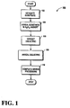
- FIG. 1 is a flow chart which illustrates a process of forming a semiconductor device in accordance with the present invention.
- FIG. 2 a is an illustration of a cross-section view of a substrate including a interlayer dielectric and a bottom capacitor electrode having a silicon nitride film formed thereon.
- FIG. 2 b is an illustration of a cross-sectional view showing the annealing of the substrate of FIG. 2 a with an H 2 /N 2 ambient.
- FIG. 2 c is an illustration of a cross-sectional view showing the formation of a dielectric film on the substrate of FIG. 2 b.
- FIG. 2 d is an illustration of a cross-sectional view showing the annealing of the dielectric film on the substrate of FIG. 2 c.
- FIG. 2 e is an illustration of a cross-sectional view showing the formation of a top capacitor electrode on the substrate o f FIG. 2 d.
- FIG. 3 is a graph which illustrates how leakage current varies for different electrode voltages for a capacitor formed with a unannealed silicon nitride layer and for a capacitor formed with a H 2 /N 2 annealed silicon nitride layer.
- FIG. 4 a is an illustration of a cross-sectional view of a substrate having a nitride film formed thereon.
- FIG. 4 b is an illustration of a cross-sectional view showing the annealing of the substrate of FIG. 4 a with a N 2 /H 2 ambient.
- FIG. 4 c is an illustration of the cross-sectional view as showing the formation of the dielectric film on the substrate of FIG. 4 b.
- FIG. 4 d is an illustration of cross-sectional view showing the annealing of the substrate of FIG. 4 c.
- FIG. 4 e is an illustration of a cross-sectional view showing the formation of a gate electrode and source/drain regions on the substrate of FIG. 4 d.
- the present invention describes a novel method and apparatus for enhancing the electrical characteristics of semiconductor devices.
- numerous specific details such as specific equipment, and process parameters are set forth in order to provide a thorough understanding of the present invention.
- One skilled in the art will appreciate the ability to use alternative configurations and process details to the disclosed specifics without departing from the scope of the present invention.
- well known semiconductor processing equipment and methodology have not been described in detail in order to not unnecessarily obscure the present invention.
- the present invention is a forming gas anneal which enhances the electrical properties of semiconductor devices.
- a thin silicon nitride film is formed on a silicon surface, such as but not limited to a monocrystalline silicon substrate or a polycrystalline capacitor electrode.
- the silicon nitride film is then annealed by heating the substrate to a temperature between 700-850° C. then exposing the substrate to an ambient comprising H 2 and preferably to a forming gas ambient (H 2 /N 2 ambient).
- the anneal step of the present invention anneals out defects at the silicon/silicon nitride interface which helps to prevent charges from becoming trapped at the interface which can lead to poor device performance such as high leakage currents and reduced capacitance.
- annealing the silicon nitride film in a forming gas ambient generally improves the quality of the silicon nitride film by curing defects in the film.
- thin, between 10-25 ⁇ , silicon nitride layers can provide robust barrier layers.
- low silicon nitride formation temperatures less than 950° C., can be used which reduces the thermal budget of a manufacturing process.
- the anneal process of the present invention enables production of high quality high performance semiconductor devices such as capacitors and transistors.
- FIG. 1 illustrates a flow chart which depicts a process of fabricating a semiconductor device in accordance with an embodiment of the present invention.
- FIGS. 2 a - 2 e illustrate an embodiment of the present invention where the forming gas anneal of the present invention is used in forming a capacitor of a DRAM cell.
- FIGS. 4 a - 4 e illustrate an embodiment of the present invention where the forming gas anneal of the present invention is used in fabricating a MOS transistor. It is to be appreciated that these specific details are only illustrative of embodiments of the present invention and are not to be taken as limiting to the present invention.
- the substrate is a substrate used in the fabrication of a dynamic random access memory (DRAM) cells such as substrate 200 shown in FIG. 2 a .
- Substrate 200 includes well known silicon epitaxial substrate 201 having a doped region 202 and a patterned interlayer dielectric 204 .
- a bottom polysilicon capacitor electrode 206 is formed in contact with the diffusion region 202 and over ILD 204 .
- Bottom capacitor electrode 206 can be formed by any well known technique such as by blanket depositing a polysilicon film by chemical vapor deposition (CVD) utilizing a reactive gas comprising silane (SiH 4 ) and H 2 and then patterning the blanket deposited material into an electrode with well known photolithography and etching techniques.
- CVD chemical vapor deposition
- bottom electrode 206 will typically be doped to a density between 2-5 ⁇ 10 20 atoms/cm 3 .
- Bottom electrode 206 can also be other types of silicon electrodes capacitor electrodes such as but not limited to hemispherical grained polysilicon (HSG) or “rough poly” electrodes.
- HSG hemispherical grained polysilicon
- monocrystalline silicon substrate 201 can act as the bottom electrode 206 .
- the first step is to nitridate substrate 200 to form a thin silicon nitride barrier layer 205 on bottom electrode 206 as shown in FIG. 2 a .
- the purpose of silicon nitride barrier layer 205 is to form an oxidation prevention barrier layer for bottom electrode 206 . In this way oxygen cannot penetrate grain boundaries of polysilicon electrode 206 and form oxides therein which can lead to a decrease in the effective dielectric constant of the capacitor dielectric and to an increase in electrode resistance.
- a thin, between 10-25 ⁇ , barrier layer can be reliably used. Utilizing a thin silicon nitride layer improves throughput and also reduces the negative capacative impact the silicon nitride layer will have on a capacitor formed with a high dielectric constant such as tantalum pentaoxide (Ta 2 O 5 ).
- a thin silicon nitride film 205 can be formed by any well know method.
- silicon nitride film 205 can be formed by thermal nitridation by placing substrate 200 into a low pressure chemical vapor deposition (LPCVD) furnace and heating substrate 200 to a temperature between 800-950° C. and exposing substrate 200 to ammonia gas (NH 3 ). Ammonia (NH 3 ) gas then reacts with exposed silicon surfaces such as polysilicon electrode 206 to form a silicon nitride (Si 3 N 4 ) film 205 .
- LPCVD low pressure chemical vapor deposition
- silicon nitride film 205 can be formed by exposing substrate 200 to highly reactive nitrogen atoms formed by disassociating NH 3 or N 2 gas with microwaves in a cavity or chamber which is remote from the chamber in which substrate 200 is located. It is to be appreciated, that because the quality of silicon nitride film 205 is to be subsequently improved with the forming gas anneal of the present invention, relatively low, less than 950° C., nitridation temperatures maybe utilized to form silicon nitride film 205 . Low nitridation temperatures are desirable because they reduce the thermal budget of the manufacturing process which is becoming increasingly important in the manufacturer of modern high density integrated circuits such as microprocessors and high density dynamic random access memories.
- substrate 200 is annealed in a forming gas (N 2 /H 2 ) ambient to form a high quality annealed silicon nitride layer 209 as shown in FIG. 2 b .
- substrate 200 can be annealed in accordance with the present invention by placing substrate 200 into a chamber of a rapid thermal processor (RTP) such as a Applied Materials RTP Centura with Honeycomb source and heated to a temperature between 700-850° C. and flowing hydrogen gas (H 2 ) and nitrogen gas (N 2 ) into the chamber to create an ambient which consist of 90-99% N 2 and 1-10% H 2 by volume.
- RTP rapid thermal processor
- Annealing substrate 200 in a RTP chamber for between 60-180 seconds suitably improves the integrity of the thin silicon nitride barrier layer 205 and improves the interface between barrier layer 205 and polysilicon electrode 206 .
- a forming gas ambient is created by flowing 1.0 slm of nitrogen gas (N 2 ) gas and 100 sccm of hydrogen gas (H 2 ) into the chamber of the processor.
- N 2 nitrogen gas
- H 2 hydrogen gas
- a rapid thermal processor is preferably used to carryout the forming gas anneal of the present invention
- the other well known apparatuses such as furnaces maybe used to anneal substrate 200 , if desired.
- substrate 200 can be annealed with a forming gas (N 2 /H 2 ) ambient at a temperature between 700-850° C. for approximately 30 minutes.
- forming gas anneal of the present invention enables the formation of a thin robust silicon nitride barrier layer 209 and enables the formation of a high quality interface between silicon nitride barrier layer 209 and polysilicon electrode 206 .
- substrate 200 preferably anneals substrate 200 in a forming gas (H 2 /N 2 ) ambient
- H 2 containing ambients may be utilized.
- substrate 200 can be annealed as described above utilizing ambient comprising hydrogen (H 2 ) and argon (Ar) or to an ambient comprising hydrogen (H 2 ) and helium (He).
- H 2 /N 2 forming gas
- substrate 200 can be annealed as described above utilizing ambient comprising hydrogen (H 2 ) and argon (Ar) or to an ambient comprising hydrogen (H 2 ) and helium (He).
- a dielectric film is formed over substrate 200 .
- a high dielectric constant dielectric film 208 is blanket deposited over ILD 204 and annealed silicon nitride film 209 formed on bottom electrode 206 of substrate 200 as shown in FIG. 2 c .
- the dielectric film is a transition metal-oxide dielectric film such as, but not limited to, tantalum pentaoxide (Ta 2 O 5 ) and titanium oxide (TiO 2 ).
- dielectric layer 208 is a tantalum pentaoxide film doped with titanium.
- dielectric layer 208 can be a composite dielectric film comprising a stack of different dielectric films such as a Ta 2 O 5 /TiO 2 /Ta 2 O 5 stacked dielectric film. Additionally, dielectric layer 208 can be a piezoelectric dielectric such as Barium Strontium Titanate (BST) and Lead Zerconium Titanate (PZT) or a ferroelectric.
- BST Barium Strontium Titanate
- PZT Lead Zerconium Titanate
- dielectric layer 208 can be a silicon-oxide dielectric such as silicon dioxide and silicon oxynitride and composite dielectric stacks of silicon-oxide and silicon nitride film such as well known ONO and NO and nitrided oxides.
- silicon-oxide dielectric such as silicon dioxide and silicon oxynitride
- composite dielectric stacks of silicon-oxide and silicon nitride film such as well known ONO and NO and nitrided oxides.
- ONO and NO and nitrided oxides are well known and can be used in the fabrication of gate dielectric layers and capacitor dielectrics.
- a low temperature silicon dioxide film can be formed by chemical vapor deposition utilizing a silicon source, such as TEOS, and an oxygen source, such as O 2 .
- the substrate can be placed into a thermal process chamber such as the chamber of an Applied Materials CVD single wafer reactor.
- the substrate is then heated to a desired deposition temperature while the pressure within the chamber is pumped down (reduced) to a desired deposition pressure.
- Deposition gases are then fed into the chamber and a dielectric layer formed therefrom.
- dielectric 208 is tantalum pentaoxide (Ta 2 O 5 ).
- a deposition gas mix comprising, a source of tantalum, such as but not limited to, TAETO [Ta(OC 2 H 5 ) 5 ] and TAT-DMAE [Ta(OC 2 H 5 ) 4 (OCHCH 2 N(CH 3 ) 2 ], and source of oxygen such as O 2 or N 2 O can be fed into a deposition chamber while the substrate is heated to a deposition temperature of between 300-500° C. and the chamber maintained at a deposition pressure of between 0.5-10 Torr.
- a source of tantalum such as but not limited to, TAETO [Ta(OC 2 H 5 ) 5 ] and TAT-DMAE [Ta(OC 2 H 5 ) 4 (OCHCH 2 N(CH 3 ) 2 ]
- source of oxygen such as O 2 or N 2 O
- TAETO or TAT-DMAE is fed into the chamber at a rate of between 10-50 milligrams per minute while O 2 or N 2 O is fed into the chamber at a rate of 0.3-1.0 SLM.
- TAETO and TAT-DMAE can be provided by direct liquid injection or vaporized with a bubbler prior to entering the deposition chamber.
- a carrier gas, such as N 2 , H 2 and He, at a rate of between 0.5-2.0 SLM can be used to transport the vaporized TAETO or TAT-DMAE liquid into the deposition chamber.
- Deposition is continued until a dielectric film 208 of a desired thickness is formed.
- a tantalum pentaoxide (Ta 2 O 5 ) dielectric film having a thickness between 50..200 ⁇ provides a suitable capacitor dielectric.
- dielectric film 208 can be annealed, if desired, to form an annealed dielectric layer 210 as shown in FIG. 2 b .
- Dielectric layer 210 can be annealed by any well known and suitable annealing process such a rapid thermal anneal or a furnace anneal in an ambient comprising an oxygen containing gas, such as O 2 or N 2 O a temperature between 800-850° C.
- dielectric film 208 can be annealed with highly reactive oxygen atoms generated by disassociating an oxygen containing gas, such as O 2 , with microwaves in a chamber which is remote or separate from the chamber in which substrate 200 is placed during the anneal.
- An anneal with reactive oxygen atoms which have been remotely generated is ideally suited for annealing a transition metal oxide dielectric film such as a tantalum pentaoxide dielectric (Ta 2 O 5 ).
- a top capacitor electrode 212 can be formed over annealed dielectric layer 210 .
- Any well known technology can be used to form top electrode 212 including blanket depositing a polysilicon film or metal film, such as TiN, over annealed dielectric film 210 and then using well known photolithography and etching techniques to pattern the electrode film and dielectric layer.
- FIG. 3 Shown in FIG. 3 are plots which illustrate how annealing silicon nitride layer 205 and bottom electrode 206 in a forming gas ambient enhances the electrical properties of the fabricated capacitor.
- FIG. 3 illustrates two plots 302 and 304 which show how leakage current varies for different top electrode voltages for capacitors formed with a structure comprising a doped polysilicon bottom electrode, a 20 ⁇ silicon nitride barrier layer, a 100 ⁇ tantalum pentaoxide dielectric which has been annealed in N 2 O for 30 seconds, and a titanium nitride top electrode.
- plot 302 the silicon nitride film/polysilicon electrode has not been treated with forming gas.
- the capacitor has good leakage current but has a low capacitance of only 9 fF/ ⁇ m 2 .
- the low capacitance is due to the formation of a silicon dioxide layer between the silicon nitride film and the polysilicon electrode.
- the oxide forms because the poor integrity of the silicon nitride barrier enables oxygen to diffuse through during the tantalum pentaoxide anneal step and cause the formation of silicon dioxide below the silicon nitride layer.
- Silicon dioxide exhibits a relatively low constant which when placed in series with the high dielectric constant transition metal-oxide dielectric causes a reduction in the effective capacitance of the capacitor.
- Plot 304 shows the electrical characteristics of a capacitor where the polysilicon electrode and silicon nitride layer have been treated with the forming gas anneal of the present invention.
- the forming gas treated capacitor exhibits essentially the same leakage current as the untreated capacitor electrode (the treated capacitor shows slightly higher leakage than the untreated capacitor due to a slightly lower anneal temperature being used for annealing the tantalum pentaoxide film).
- the capacitor treated with the forming gas however exhibits a significantly higher capacitance of 11 fF/ ⁇ m 2 .
- the forming gas treated capacitor exhibits higher capacitance because the silicon nitride barrier is more robust due to the forming gas treatment and therefore oxygen is unable to penetrate it during the tantalum pentaoxide anneal step. Since oxygen penetration is eliminated or substantially reduced a silicon oxide layer is unable to form between the silicon nitride film and the polysilicon electrode. In this way a forming gas treated capacitor exhibits higher capacitance than an untreated capacitor. Additionally, the forming gas anneal of the present invention improves the interface between the silicon nitride layer and the polysilicon gate electrode which helps to improve the capacitance.
- the forming gas anneal of the present invention is used in fabricating a metal insulator semiconductor (MIS) transistor.
- the first step as shown in FIG. 4 a is to nitridate a monocrystalline silicon substrate 402 to form a thin, 10-25 ⁇ , silicon nitride film 401 on substrate 402 .
- substrate 400 is annealed with forming gas (N 2 /H 2 ) gas as described above to form a robust annealed silicon nitride barrier layer 403 and to cure any defects which may exist at the silicon substrate/silicon nitride interface.
- forming gas N 2 /H 2
- a dielectric layer 404 is formed on annealed silicon nitride layer 403 .
- Dielectric layer 404 can be any dielectric film such as a CVD deposited silicon dioxide film, or transition metal oxide film such as tantalum pentaoxide. Dielectric 404 will typically have a thickness between 20-100 ⁇ .
- dielectric film 404 can be annealed if desired.
- a gate electrode material such as polysilicon or metal or combination thereof, can be blanket deposited over annealed dielectric 406 and then patterned into a gate electrode 408 as shown in FIG. 4 d with well known photolithography and etching techniques.
- a pair of source/drain regions 410 can then be formed on opposites sides of gate electrode 408 with well known ion implantation or solid source diffusion techniques in order to complete fabrication of the MOS device.
Abstract
A method for improving the interface between a silicon nitride film and a silicon surface is described. According to the present invention a silicon nitride film is formed on a silicon surface of a substrate. While said substrate is heated the silicon nitride film is exposed to an ambient comprising hydrogen (H2). In a prefered embodiment of the present invention the ambient comprises H2 and N2.
Description
This is a Divisional Application of Serial No.: 09/152,871 filed Sep. 14, 1998, which is now U.S. Pat. No. 6,037,235.
1. Field of the Invention
The present invention relates to the field of semiconductor manufacturing and more specifically to a method and apparatus for improving the electrical characteristic of semiconductor devices.
2. Discussion of Related Art
Integrated circuits are made up of literally millions of active and passive devices such as transistors, capacitors and resistors. In order to provide more computational power and/or more storage capability in an integrated circuit, device features are reduced or scaled down in order to provide higher packing density of devices. An important feature to enable scaling of devices is the ability to form high quality, high dielectric constant films for capacitor and gate dielectrics.
High dielectric constant films are generally ceramic films (i.e., metaloxides) such as tantalum pentaoxide and titanium oxide. When these films are deposited they tend to have vacancies at the anionic (oxygen) sites in the lattice. Presently these vacancies are filled by annealing the film in an oxygen containing gas. However, such an anneal causes the oxidation of the underlying polysilicon electrode in the case of a capacitor and the oxidation of the underlying silicon substrate in the case of a MOS transistor. Such an oxidation of the underlying silicon layer causes the formation of a silicon dioxide film in series with the high dielectric constant film which in turn reduces the effective dielectric constant of the combined film.
As such, in order to integrate a high dielectric constant film, such as tantalum pentaoxide, into a capacitor or MOS fabrication scheme, it has been found important to form a silicon nitride barrier layer between the high dielectric constant material and the silicon surface in order to prevent oxidation of the underlying silicon surface and a corresponding reduction in the effective capacitance of the device. The silicon nitride barrier layer, however, needs to be formed thin, between 10-25 Å, so that its low dielectric constant does not decrease the effective dielectric constant of the high dielectric constant film. Additionally, the silicon nitride film needs to be formed at low temperatures, less than 950° C., in order to keep the thermal budget of the fabrication process low. Unfortunately, however, a thin silicon nitride layer formed at a low nitridation temperature creates a poor quality barrier to oxygen diffusion. Additionally, defects such as dangling bonds can be created at the silicon nitride/silicon surface interface. Such dangling bonds can lead to poor device performance such as increased leakage currents and reduced capacitance.
Thus, what is needed is a method of forming a thin robust silicon nitride barrier layer at a relatively low temperature and a method which can cure defects at the silicon nitride/silicon surface interface.
A method for improving the interface between a silicon nitride film and a silicon surface is described. According to the present invention a silicon nitride film is formed on a silicon surface of a substrate. While said substrate is heated the silicon nitride film is exposed to an ambient comprising hydrogen (H2). In a prefered embodiment of the present invention the ambient comprises H2 and N2.
FIG. 1 is a flow chart which illustrates a process of forming a semiconductor device in accordance with the present invention.
FIG. 2a is an illustration of a cross-section view of a substrate including a interlayer dielectric and a bottom capacitor electrode having a silicon nitride film formed thereon.
FIG. 2b is an illustration of a cross-sectional view showing the annealing of the substrate of FIG. 2a with an H2/N2 ambient.
FIG. 2c is an illustration of a cross-sectional view showing the formation of a dielectric film on the substrate of FIG. 2b.
FIG. 2d is an illustration of a cross-sectional view showing the annealing of the dielectric film on the substrate of FIG. 2c.
FIG. 2e is an illustration of a cross-sectional view showing the formation of a top capacitor electrode on the substrate o f FIG. 2d.
FIG. 3 is a graph which illustrates how leakage current varies for different electrode voltages for a capacitor formed with a unannealed silicon nitride layer and for a capacitor formed with a H2/N2 annealed silicon nitride layer.
FIG. 4a is an illustration of a cross-sectional view of a substrate having a nitride film formed thereon.
FIG. 4b is an illustration of a cross-sectional view showing the annealing of the substrate of FIG. 4a with a N2/H2 ambient.
FIG. 4c is an illustration of the cross-sectional view as showing the formation of the dielectric film on the substrate of FIG. 4b.
FIG. 4d is an illustration of cross-sectional view showing the annealing of the substrate of FIG. 4c.
FIG. 4e is an illustration of a cross-sectional view showing the formation of a gate electrode and source/drain regions on the substrate of FIG. 4d.
The present invention describes a novel method and apparatus for enhancing the electrical characteristics of semiconductor devices. In the following description numerous specific details such as specific equipment, and process parameters are set forth in order to provide a thorough understanding of the present invention. One skilled in the art will appreciate the ability to use alternative configurations and process details to the disclosed specifics without departing from the scope of the present invention. In other instances, well known semiconductor processing equipment and methodology have not been described in detail in order to not unnecessarily obscure the present invention.
The present invention is a forming gas anneal which enhances the electrical properties of semiconductor devices. According to the present invention, a thin silicon nitride film is formed on a silicon surface, such as but not limited to a monocrystalline silicon substrate or a polycrystalline capacitor electrode. The silicon nitride film is then annealed by heating the substrate to a temperature between 700-850° C. then exposing the substrate to an ambient comprising H2 and preferably to a forming gas ambient (H2/N2 ambient). The anneal step of the present invention anneals out defects at the silicon/silicon nitride interface which helps to prevent charges from becoming trapped at the interface which can lead to poor device performance such as high leakage currents and reduced capacitance. Additionally, annealing the silicon nitride film in a forming gas ambient generally improves the quality of the silicon nitride film by curing defects in the film. By improving the quality of the silicon nitride film, thin, between 10-25 Å, silicon nitride layers can provide robust barrier layers. Additionally, because the quality of the silicon nitride film is subsequently improved with an anneal step, low silicon nitride formation temperatures, less than 950° C., can be used which reduces the thermal budget of a manufacturing process. The anneal process of the present invention enables production of high quality high performance semiconductor devices such as capacitors and transistors.
A method of fabricating a semiconductor device in accordance with the present invention will be described in reference to FIG. 1 and FIGS. 2a-2 e. FIG. 1 illustrates a flow chart which depicts a process of fabricating a semiconductor device in accordance with an embodiment of the present invention. FIGS. 2a-2 e illustrate an embodiment of the present invention where the forming gas anneal of the present invention is used in forming a capacitor of a DRAM cell. FIGS. 4a-4 e illustrate an embodiment of the present invention where the forming gas anneal of the present invention is used in fabricating a MOS transistor. It is to be appreciated that these specific details are only illustrative of embodiments of the present invention and are not to be taken as limiting to the present invention.
In one embodiment of the present invention, the substrate is a substrate used in the fabrication of a dynamic random access memory (DRAM) cells such as substrate 200 shown in FIG. 2a. Substrate 200 includes well known silicon epitaxial substrate 201 having a doped region 202 and a patterned interlayer dielectric 204. A bottom polysilicon capacitor electrode 206 is formed in contact with the diffusion region 202 and over ILD 204. Bottom capacitor electrode 206 can be formed by any well known technique such as by blanket depositing a polysilicon film by chemical vapor deposition (CVD) utilizing a reactive gas comprising silane (SiH4) and H2 and then patterning the blanket deposited material into an electrode with well known photolithography and etching techniques. If bottom electrode 206 will typically be doped to a density between 2-5×10²⁰ atoms/cm3. Bottom electrode 206 can also be other types of silicon electrodes capacitor electrodes such as but not limited to hemispherical grained polysilicon (HSG) or “rough poly” electrodes. In still other cases, as is well known in the art, monocrystalline silicon substrate 201 can act as the bottom electrode 206.
The first step, as set forth in block 102 of flow chart 100, is to nitridate substrate 200 to form a thin silicon nitride barrier layer 205 on bottom electrode 206 as shown in FIG. 2a. The purpose of silicon nitride barrier layer 205 is to form an oxidation prevention barrier layer for bottom electrode 206. In this way oxygen cannot penetrate grain boundaries of polysilicon electrode 206 and form oxides therein which can lead to a decrease in the effective dielectric constant of the capacitor dielectric and to an increase in electrode resistance. Because defects, such as pinholes, formed in silicon nitride film 205, are to be subsequently cured by the forming gas anneal of the present invention, a thin, between 10-25 Å, barrier layer can be reliably used. Utilizing a thin silicon nitride layer improves throughput and also reduces the negative capacative impact the silicon nitride layer will have on a capacitor formed with a high dielectric constant such as tantalum pentaoxide (Ta2O5).
A thin silicon nitride film 205 can be formed by any well know method. For example, silicon nitride film 205 can be formed by thermal nitridation by placing substrate 200 into a low pressure chemical vapor deposition (LPCVD) furnace and heating substrate 200 to a temperature between 800-950° C. and exposing substrate 200 to ammonia gas (NH3). Ammonia (NH3) gas then reacts with exposed silicon surfaces such as polysilicon electrode 206 to form a silicon nitride (Si3N4) film 205. Alternatively, silicon nitride film 205 can be formed by exposing substrate 200 to highly reactive nitrogen atoms formed by disassociating NH3 or N2 gas with microwaves in a cavity or chamber which is remote from the chamber in which substrate 200 is located. It is to be appreciated, that because the quality of silicon nitride film 205 is to be subsequently improved with the forming gas anneal of the present invention, relatively low, less than 950° C., nitridation temperatures maybe utilized to form silicon nitride film 205. Low nitridation temperatures are desirable because they reduce the thermal budget of the manufacturing process which is becoming increasingly important in the manufacturer of modern high density integrated circuits such as microprocessors and high density dynamic random access memories.
Next, as set forth in block 104 a flow chart 100, substrate 200 is annealed in a forming gas (N2/H2) ambient to form a high quality annealed silicon nitride layer 209 as shown in FIG. 2b. Substrate 200 can be annealed in accordance with the present invention by placing substrate 200 into a chamber of a rapid thermal processor (RTP) such as a Applied Materials RTP Centura with Honeycomb source and heated to a temperature between 700-850° C. and flowing hydrogen gas (H2) and nitrogen gas (N2) into the chamber to create an ambient which consist of 90-99% N2 and 1-10% H2 by volume. Annealing substrate 200 in a RTP chamber for between 60-180 seconds suitably improves the integrity of the thin silicon nitride barrier layer 205 and improves the interface between barrier layer 205 and polysilicon electrode 206. In one embodiment of the present invention a forming gas ambient is created by flowing 1.0 slm of nitrogen gas (N2) gas and 100 sccm of hydrogen gas (H2) into the chamber of the processor. Although a rapid thermal processor is preferably used to carryout the forming gas anneal of the present invention, the other well known apparatuses such as furnaces maybe used to anneal substrate 200, if desired. In the case of a furnace anneal, substrate 200 can be annealed with a forming gas (N2/H2) ambient at a temperature between 700-850° C. for approximately 30 minutes.
By heating and exposing substrate 200 to hydrogen gas and nitrogen gas, defects such as pinholes in silicon nitride film 205 are eliminated or substantially reduced. In this way oxygen cannot penetrate through silicon nitride barrier layer 209 and oxidize silicon electrode 206. Additionally, annealing substrate 200 with forming gas provides hydrogen which can defuse through silicon nitride layer 205 and cure defects, such as dangling bonds, at the silicon nitride 205/polysilicon electrode 206 interface which could otherwise trap charges and cause poor device performance such as high leakage currents. Thus, the forming gas anneal of the present invention enables the formation of a thin robust silicon nitride barrier layer 209 and enables the formation of a high quality interface between silicon nitride barrier layer 209 and polysilicon electrode 206.
Although the present invention preferably anneals substrate 200 in a forming gas (H2/N2) ambient other hydrogen (H2) containing ambients may be utilized. For example substrate 200 can be annealed as described above utilizing ambient comprising hydrogen (H2) and argon (Ar) or to an ambient comprising hydrogen (H2) and helium (He). Additionally, it is also possible to anneal substrate 200 in an ambient consisting of 100% and obtain benefits as described above.
Next, as set forth in block 106, a dielectric film is formed over substrate 200. In one embodiment of the present invention a high dielectric constant dielectric film 208 is blanket deposited over ILD 204 and annealed silicon nitride film 209 formed on bottom electrode 206 of substrate 200 as shown in FIG. 2c. In a preferred embodiment of the present invention the dielectric film is a transition metal-oxide dielectric film such as, but not limited to, tantalum pentaoxide (Ta2O5) and titanium oxide (TiO2). In another embodiment dielectric layer 208 is a tantalum pentaoxide film doped with titanium. Additionally dielectric layer 208 can be a composite dielectric film comprising a stack of different dielectric films such as a Ta2O5/TiO2/Ta2O5 stacked dielectric film. Additionally, dielectric layer 208 can be a piezoelectric dielectric such as Barium Strontium Titanate (BST) and Lead Zerconium Titanate (PZT) or a ferroelectric.
In other embodiments of the present invention dielectric layer 208 can be a silicon-oxide dielectric such as silicon dioxide and silicon oxynitride and composite dielectric stacks of silicon-oxide and silicon nitride film such as well known ONO and NO and nitrided oxides. The fabrication of such oxides are well known and can be used in the fabrication of gate dielectric layers and capacitor dielectrics. For example, a low temperature silicon dioxide film can be formed by chemical vapor deposition utilizing a silicon source, such as TEOS, and an oxygen source, such as O2.
In order to form a dielectric layer 208 onto substrate 200, the substrate can be placed into a thermal process chamber such as the chamber of an Applied Materials CVD single wafer reactor. The substrate is then heated to a desired deposition temperature while the pressure within the chamber is pumped down (reduced) to a desired deposition pressure. Deposition gases are then fed into the chamber and a dielectric layer formed therefrom.
In a preferred embodiment of the present invention dielectric 208 is tantalum pentaoxide (Ta2O5). To blanket deposit a tantalum pentaoxide (Ta2O5) dielectric film by thermal chemical vapor deposition a deposition gas mix comprising, a source of tantalum, such as but not limited to, TAETO [Ta(OC2H5)5] and TAT-DMAE [Ta(OC2H5)4(OCHCH2N(CH3)2], and source of oxygen such as O2 or N2O can be fed into a deposition chamber while the substrate is heated to a deposition temperature of between 300-500° C. and the chamber maintained at a deposition pressure of between 0.5-10 Torr. The flow of deposition gas over the heated substrate results in thermal decomposition of the metal organic Ta-containing precursor an subsequent deposition of a tantalum pentaoxide film. In one embodiment TAETO or TAT-DMAE is fed into the chamber at a rate of between 10-50 milligrams per minute while O2 or N2O is fed into the chamber at a rate of 0.3-1.0 SLM. TAETO and TAT-DMAE can be provided by direct liquid injection or vaporized with a bubbler prior to entering the deposition chamber. A carrier gas, such as N2, H2 and He, at a rate of between 0.5-2.0 SLM can be used to transport the vaporized TAETO or TAT-DMAE liquid into the deposition chamber. Deposition is continued until a dielectric film 208 of a desired thickness is formed. A tantalum pentaoxide (Ta2O5) dielectric film having a thickness between 50‥200 Å provides a suitable capacitor dielectric.
Next, as set forth in block 108 of flow chart 100, dielectric film 208 can be annealed, if desired, to form an annealed dielectric layer 210 as shown in FIG. 2b. Dielectric layer 210 can be annealed by any well known and suitable annealing process such a rapid thermal anneal or a furnace anneal in an ambient comprising an oxygen containing gas, such as O2 or N2O a temperature between 800-850° C. Alternatively, dielectric film 208 can be annealed with highly reactive oxygen atoms generated by disassociating an oxygen containing gas, such as O2, with microwaves in a chamber which is remote or separate from the chamber in which substrate 200 is placed during the anneal. An anneal with reactive oxygen atoms which have been remotely generated is ideally suited for annealing a transition metal oxide dielectric film such as a tantalum pentaoxide dielectric (Ta2O5).
The next step of the present invention, as set forth in block 110 of flow chart 100 is to complete the processing of the device. For example, as shown in FIG. 2e, a top capacitor electrode 212 can be formed over annealed dielectric layer 210. Any well known technology can be used to form top electrode 212 including blanket depositing a polysilicon film or metal film, such as TiN, over annealed dielectric film 210 and then using well known photolithography and etching techniques to pattern the electrode film and dielectric layer.
Shown in FIG. 3 are plots which illustrate how annealing silicon nitride layer 205 and bottom electrode 206 in a forming gas ambient enhances the electrical properties of the fabricated capacitor. FIG. 3 illustrates two plots 302 and 304 which show how leakage current varies for different top electrode voltages for capacitors formed with a structure comprising a doped polysilicon bottom electrode, a 20 Å silicon nitride barrier layer, a 100 Å tantalum pentaoxide dielectric which has been annealed in N2O for 30 seconds, and a titanium nitride top electrode. In plot 302 the silicon nitride film/polysilicon electrode has not been treated with forming gas. As can be seen from the plot 302, the capacitor has good leakage current but has a low capacitance of only 9 fF/μm2. The low capacitance is due to the formation of a silicon dioxide layer between the silicon nitride film and the polysilicon electrode. The oxide forms because the poor integrity of the silicon nitride barrier enables oxygen to diffuse through during the tantalum pentaoxide anneal step and cause the formation of silicon dioxide below the silicon nitride layer. Silicon dioxide exhibits a relatively low constant which when placed in series with the high dielectric constant transition metal-oxide dielectric causes a reduction in the effective capacitance of the capacitor. Plot 304 on the other hand shows the electrical characteristics of a capacitor where the polysilicon electrode and silicon nitride layer have been treated with the forming gas anneal of the present invention. As can be seen from plot 304, the forming gas treated capacitor exhibits essentially the same leakage current as the untreated capacitor electrode (the treated capacitor shows slightly higher leakage than the untreated capacitor due to a slightly lower anneal temperature being used for annealing the tantalum pentaoxide film). The capacitor treated with the forming gas however exhibits a significantly higher capacitance of 11 fF/μm2. The forming gas treated capacitor exhibits higher capacitance because the silicon nitride barrier is more robust due to the forming gas treatment and therefore oxygen is unable to penetrate it during the tantalum pentaoxide anneal step. Since oxygen penetration is eliminated or substantially reduced a silicon oxide layer is unable to form between the silicon nitride film and the polysilicon electrode. In this way a forming gas treated capacitor exhibits higher capacitance than an untreated capacitor. Additionally, the forming gas anneal of the present invention improves the interface between the silicon nitride layer and the polysilicon gate electrode which helps to improve the capacitance.
In another embodiment of the present invention as shown in FIGS. 4a-4 e, the forming gas anneal of the present invention is used in fabricating a metal insulator semiconductor (MIS) transistor. The first step as shown in FIG. 4a, is to nitridate a monocrystalline silicon substrate 402 to form a thin, 10-25 Å, silicon nitride film 401 on substrate 402. Next, as shown in FIG. 4b, substrate 400 is annealed with forming gas (N2/H2) gas as described above to form a robust annealed silicon nitride barrier layer 403 and to cure any defects which may exist at the silicon substrate/silicon nitride interface. Next, as shown in FIG. 4c, a dielectric layer 404 is formed on annealed silicon nitride layer 403. Dielectric layer 404 can be any dielectric film such as a CVD deposited silicon dioxide film, or transition metal oxide film such as tantalum pentaoxide. Dielectric 404 will typically have a thickness between 20-100 Å. Next, as shown in FIG. 4c, dielectric film 404 can be annealed if desired. Next, a gate electrode material, such as polysilicon or metal or combination thereof, can be blanket deposited over annealed dielectric 406 and then patterned into a gate electrode 408 as shown in FIG. 4d with well known photolithography and etching techniques. A pair of source/drain regions 410 can then be formed on opposites sides of gate electrode 408 with well known ion implantation or solid source diffusion techniques in order to complete fabrication of the MOS device.
Thus, a method and apparatus for enhancing the electrical performance of semiconductor devices has been described.
Claims (10)
1. A method of forming a semiconductor transistor comprising steps of:
exposing a substrate having a silicon nitride film formed on a silicon surface to an ambient comprising hydrogen (H2) and nitrogen (N2) while heating said substrate; and
forming a dielectric layer on said ambient exposed silicon nitride film,
forming a gate electrode over said dielectric layer; and
forming a pair of source/drain regions on opposite sides of said gate electrode.
2. The method of claim 1 wherein said ambient comprises less than 10% hydrogen by volume and more than 90% nitrogen by volume.
3. The method of claim 1 further comprising the step of heating said substrate to a temperature between 700-850° C. while exposing said silicon nitride film to said ambient.
4. The method of claim 1 wherein said silicon surface is a doped polysilicon film.
5. The method of claim 1 wherein said silicon surface monocrystalline silicon.
6. The method of claim 1 wherein said silicon nitride film has a thickness between 10-25 Å.
7. The method of claim 1 wherein said dielectric is a transition metal oxide dielectric.
8. The method of claim 1 wherein said silicon nitride film is exposed aid ambient for between 60-180 seconds.
9. The method of claim 1 further comprising the step of annealing said electric layer.
10. A method of forming a metal insulated semiconductor (MIS) transistor, said method comprising the steps of:
forming a silicon nitride film on a monocrystalline silicon surface of a substrate;
heating said substrate to a temperature between 700-850° C;
while heating said substrate, exposing said substrate to an ambient comprising hydrogen (H2) and nitrogen (N2);
forming a dielectric layer on said ambient exposed silicon nitride layer;
forming a gate electrode over said dielectric layer; and
forming a pair of source/drain regions on opposite sides of said gate electrode.
Priority Applications (1)
| Application Number | Priority Date | Filing Date | Title |
|---|---|---|---|
| US09/499,336 US6387761B1 (en) | 1998-09-14 | 2000-02-04 | Anneal for enhancing the electrical characteristic of semiconductor devices |
Applications Claiming Priority (2)
| Application Number | Priority Date | Filing Date | Title |
|---|---|---|---|
| US09/152,871 US6037235A (en) | 1998-09-14 | 1998-09-14 | Hydrogen anneal for curing defects of silicon/nitride interfaces of semiconductor devices |
| US09/499,336 US6387761B1 (en) | 1998-09-14 | 2000-02-04 | Anneal for enhancing the electrical characteristic of semiconductor devices |
Related Parent Applications (1)
| Application Number | Title | Priority Date | Filing Date |
|---|---|---|---|
| US09/152,871 Continuation US6037235A (en) | 1998-09-14 | 1998-09-14 | Hydrogen anneal for curing defects of silicon/nitride interfaces of semiconductor devices |
Publications (1)
| Publication Number | Publication Date |
|---|---|
| US6387761B1 true US6387761B1 (en) | 2002-05-14 |
Family
ID=22544812
Family Applications (2)
| Application Number | Title | Priority Date | Filing Date |
|---|---|---|---|
| US09/152,871 Expired - Fee Related US6037235A (en) | 1998-09-14 | 1998-09-14 | Hydrogen anneal for curing defects of silicon/nitride interfaces of semiconductor devices |
| US09/499,336 Expired - Fee Related US6387761B1 (en) | 1998-09-14 | 2000-02-04 | Anneal for enhancing the electrical characteristic of semiconductor devices |
Family Applications Before (1)
| Application Number | Title | Priority Date | Filing Date |
|---|---|---|---|
| US09/152,871 Expired - Fee Related US6037235A (en) | 1998-09-14 | 1998-09-14 | Hydrogen anneal for curing defects of silicon/nitride interfaces of semiconductor devices |
Country Status (1)
| Country | Link |
|---|---|
| US (2) | US6037235A (en) |
Cited By (23)
| Publication number | Priority date | Publication date | Assignee | Title |
|---|---|---|---|---|
| US20020192979A1 (en) * | 2001-06-13 | 2002-12-19 | Ahn Kie Y. | Dielectric layer forming method and devices formed therewith |
| US6544908B1 (en) * | 2000-08-30 | 2003-04-08 | Micron Technology, Inc. | Ammonia gas passivation on nitride encapsulated devices |
| US20030129806A1 (en) * | 2000-10-17 | 2003-07-10 | Hitachi, Ltd. | Production of semiconductor integrated circuit |
| US20030157769A1 (en) * | 2000-04-06 | 2003-08-21 | Weimer Ronald A. | Method of fabricating an integrated circuit with a dielectric layer exposed to a hydrogen-bearing nitrogen source |
| US20030178674A1 (en) * | 2002-03-22 | 2003-09-25 | Shigeru Fujita | Semiconductor device and its manufacturing method |
| US20030232491A1 (en) * | 2002-06-18 | 2003-12-18 | Fujitsu Limited | Semiconductor device fabrication method |
| US20040092073A1 (en) * | 2002-11-08 | 2004-05-13 | Cyril Cabral | Deposition of hafnium oxide and/or zirconium oxide and fabrication of passivated electronic structures |
| US20040110352A1 (en) * | 2002-12-10 | 2004-06-10 | Texas Instruments Incorporated | Source drain and extension dopant concentration |
| US20040229475A1 (en) * | 2003-05-13 | 2004-11-18 | Bevan Malcolm J. | System and method for mitigating oxide growth in a gate dielectric |
| US20040266117A1 (en) * | 2003-06-30 | 2004-12-30 | Hwang Hyun Sang | Method of manufacturing high-k gate dielectric by use of annealing in high-pressure hydrogen atmosphere |
| US20050121671A1 (en) * | 2002-10-21 | 2005-06-09 | Taiwan Semiconductor Manufacturing Co., Ltd. | Method for fabricating laminated silicon gate electrode |
| US20050159008A1 (en) * | 2004-01-15 | 2005-07-21 | Taiwan Semiconductor Manufacturing Co. | High temperature hydrogen annealing of a gate insulator layer to increase etching selectivity between conductive gate structure and gate insulator layer |
| US20050186765A1 (en) * | 2004-02-23 | 2005-08-25 | Yi Ma | Gate electrode dopant activation method for semiconductor manufacturing |
| US20060018639A1 (en) * | 2003-10-27 | 2006-01-26 | Sundar Ramamurthy | Processing multilayer semiconductors with multiple heat sources |
| US20060169669A1 (en) * | 2005-01-31 | 2006-08-03 | Applied Materials, Inc. | Etchant treatment processes for substrate surfaces and chamber surfaces |
| US20060175671A1 (en) * | 2005-02-08 | 2006-08-10 | Taiwan Semiconductor Manufacturing Company, Ltd. | MOSFET having a channel mechanically stressed by an epitaxially grown, high k strain layer |
| US20060234488A1 (en) * | 2003-10-10 | 2006-10-19 | Yihwan Kim | METHODS OF SELECTIVE DEPOSITION OF HEAVILY DOPED EPITAXIAL SiGe |
| US20070066023A1 (en) * | 2005-09-20 | 2007-03-22 | Randhir Thakur | Method to form a device on a soi substrate |
| US20070263340A1 (en) * | 1999-03-01 | 2007-11-15 | Micron Technology, Inc. | Thin film structure that may be used with an adhesion layer |
| US20140306317A1 (en) * | 2013-04-15 | 2014-10-16 | Globalfoundries Inc. | Finfet fin height control |
| US9245767B2 (en) | 2013-09-12 | 2016-01-26 | Applied Materials, Inc. | Anneal module for semiconductor wafers |
| US9337044B2 (en) | 2003-05-13 | 2016-05-10 | Texas Instruments Incorporated | System and method for mitigating oxide growth in a gate dielectric |
| US9425054B2 (en) * | 2014-06-26 | 2016-08-23 | SK Hynix Inc. | Method for fabricating semiconductor device |
Families Citing this family (23)
| Publication number | Priority date | Publication date | Assignee | Title |
|---|---|---|---|---|
| US6228701B1 (en) * | 1997-12-19 | 2001-05-08 | Seimens Aktiengesellschaft | Apparatus and method for minimizing diffusion in stacked capacitors formed on silicon plugs |
| JP3189813B2 (en) * | 1998-11-30 | 2001-07-16 | 日本電気株式会社 | Method for manufacturing semiconductor device |
| JP3251256B2 (en) | 1999-03-01 | 2002-01-28 | 沖電気工業株式会社 | Method for manufacturing semiconductor device |
| US6417041B1 (en) * | 1999-03-26 | 2002-07-09 | Advanced Micro Devices, Inc. | Method for fabricating high permitivity dielectric stacks having low buffer oxide |
| US6221712B1 (en) * | 1999-08-30 | 2001-04-24 | United Microelectronics Corp. | Method for fabricating gate oxide layer |
| US6171911B1 (en) * | 1999-09-13 | 2001-01-09 | Taiwan Semiconductor Manufacturing Company | Method for forming dual gate oxides on integrated circuits with advanced logic devices |
| US6451646B1 (en) * | 2000-08-30 | 2002-09-17 | Micron Technology, Inc. | High-k dielectric materials and processes for manufacturing them |
| US6750157B1 (en) * | 2000-10-12 | 2004-06-15 | Advanced Micro Devices, Inc. | Nonvolatile memory cell with a nitridated oxide layer |
| US7378719B2 (en) * | 2000-12-20 | 2008-05-27 | Micron Technology, Inc. | Low leakage MIM capacitor |
| KR100385952B1 (en) | 2001-01-19 | 2003-06-02 | 삼성전자주식회사 | A semiconductor capacitor having tantalum oxide as dielctric film and formation method thereof |
| DE10296448T5 (en) * | 2001-03-20 | 2004-04-15 | Mattson Technology Inc., Fremont | A method of depositing a layer having a relatively high dielectric constant on a substrate |
| US6495475B2 (en) | 2001-03-28 | 2002-12-17 | Atmel Corporation | Method for fabrication of a high capacitance interpoly dielectric |
| US6531368B1 (en) * | 2001-04-03 | 2003-03-11 | Advanced Micro Devices, Inc. | Method of fabricating a semiconductor device having a metal oxide high-k gate insulator by localized laser irradiation and a device thereby formed |
| US7026229B2 (en) * | 2001-11-28 | 2006-04-11 | Vartan Semiconductor Equipment Associates, Inc. | Athermal annealing with rapid thermal annealing system and method |
| DE10392519T5 (en) * | 2002-04-19 | 2005-08-04 | Mattson Technology Inc., Fremont | A system for depositing a film on a substrate using a low vapor pressure gas precursor |
| US20040247787A1 (en) * | 2002-04-19 | 2004-12-09 | Mackie Neil M. | Effluent pressure control for use in a processing system |
| US6611449B1 (en) * | 2002-09-24 | 2003-08-26 | Infineon Technologies Aktiengesellschaft | Contact for memory cells |
| TW566366U (en) * | 2002-09-27 | 2003-12-11 | Wus Tech Co Ltd | Labor-saving portable battery equipment for power-driven walking assisted scooter |
| US6858442B2 (en) * | 2003-02-25 | 2005-02-22 | Infineon Technologies Aktiengesellschaft | Ferroelectric memory integrated circuit with improved reliability |
| US20080199995A1 (en) * | 2007-02-15 | 2008-08-21 | Debra Susan Woolsey | Integrated Hydrogen Anneal and Gate Oxidation for Improved Gate Oxide Integrity |
| US8252653B2 (en) * | 2008-10-21 | 2012-08-28 | Applied Materials, Inc. | Method of forming a non-volatile memory having a silicon nitride charge trap layer |
| US8198671B2 (en) * | 2009-04-22 | 2012-06-12 | Applied Materials, Inc. | Modification of charge trap silicon nitride with oxygen plasma |
| US11251261B2 (en) * | 2019-05-17 | 2022-02-15 | Micron Technology, Inc. | Forming a barrier material on an electrode |
Citations (6)
| Publication number | Priority date | Publication date | Assignee | Title |
|---|---|---|---|---|
| US4983544A (en) | 1986-10-20 | 1991-01-08 | International Business Machines Corporation | Silicide bridge contact process |
| US5405801A (en) | 1992-02-28 | 1995-04-11 | Samsung Electronics Co., Ltd. | Method for manufacturing a capacitor of a semiconductor device |
| US5550091A (en) | 1993-07-14 | 1996-08-27 | Frontec Incorporated | Method of sputtering a silicon nitride film |
| US5591681A (en) | 1994-06-03 | 1997-01-07 | Advanced Micro Devices, Inc. | Method for achieving a highly reliable oxide film |
| US5629043A (en) | 1994-12-15 | 1997-05-13 | Mitsubishi Denki Kabushiki Kaisha | Silicon nitride film formation method |
| US5716875A (en) * | 1996-03-01 | 1998-02-10 | Motorola, Inc. | Method for making a ferroelectric device |
-
1998
- 1998-09-14 US US09/152,871 patent/US6037235A/en not_active Expired - Fee Related
-
2000
- 2000-02-04 US US09/499,336 patent/US6387761B1/en not_active Expired - Fee Related
Patent Citations (6)
| Publication number | Priority date | Publication date | Assignee | Title |
|---|---|---|---|---|
| US4983544A (en) | 1986-10-20 | 1991-01-08 | International Business Machines Corporation | Silicide bridge contact process |
| US5405801A (en) | 1992-02-28 | 1995-04-11 | Samsung Electronics Co., Ltd. | Method for manufacturing a capacitor of a semiconductor device |
| US5550091A (en) | 1993-07-14 | 1996-08-27 | Frontec Incorporated | Method of sputtering a silicon nitride film |
| US5591681A (en) | 1994-06-03 | 1997-01-07 | Advanced Micro Devices, Inc. | Method for achieving a highly reliable oxide film |
| US5629043A (en) | 1994-12-15 | 1997-05-13 | Mitsubishi Denki Kabushiki Kaisha | Silicon nitride film formation method |
| US5716875A (en) * | 1996-03-01 | 1998-02-10 | Motorola, Inc. | Method for making a ferroelectric device |
Non-Patent Citations (1)
| Title |
|---|
| Wolf, S. and Tauber, R.N.; Silicon Processing for the VLSI Era; vol. 1; Lattice Press; Sunset Beach, CA.; p. 194. |
Cited By (74)
| Publication number | Priority date | Publication date | Assignee | Title |
|---|---|---|---|---|
| US20070263340A1 (en) * | 1999-03-01 | 2007-11-15 | Micron Technology, Inc. | Thin film structure that may be used with an adhesion layer |
| US8593784B2 (en) * | 1999-03-01 | 2013-11-26 | Round Rock Research, Llc | Thin film structure that may be used with an adhesion layer |
| US20040164344A1 (en) * | 2000-04-06 | 2004-08-26 | Weimer Ronald A. | Method of fabricating an integrated circuit with a dielectric layer exposed to a hydrogen-bearing nitrogen source |
| US6924197B2 (en) | 2000-04-06 | 2005-08-02 | Micron Technology, Inc. | Method of fabricating an integrated circuit with a dielectric layer exposed to a hydrogen-bearing nitrogen source |
| US20030157769A1 (en) * | 2000-04-06 | 2003-08-21 | Weimer Ronald A. | Method of fabricating an integrated circuit with a dielectric layer exposed to a hydrogen-bearing nitrogen source |
| US6921937B2 (en) | 2000-04-06 | 2005-07-26 | Micron Technology, Inc. | Integrated circuit with a dielectric layer exposed to a hydrogen-bearing nitrogen source |
| US7087182B2 (en) | 2000-04-06 | 2006-08-08 | Micron Technology, Inc. | Process of forming an electrically erasable programmable read only memory with an oxide layer exposed to hydrogen and nitrogen |
| US6815805B2 (en) | 2000-04-06 | 2004-11-09 | Micron Technology, Inc. | Method of fabricating an integrated circuit with a dielectric layer exposed to a hydrogen-bearing nitrogen source |
| US6544908B1 (en) * | 2000-08-30 | 2003-04-08 | Micron Technology, Inc. | Ammonia gas passivation on nitride encapsulated devices |
| US20030157815A1 (en) * | 2000-08-30 | 2003-08-21 | Weimer Ronald A. | Ammonia gas passivation on nitride encapsulated devices |
| US6908868B2 (en) | 2000-08-30 | 2005-06-21 | Micron Technology, Inc. | Gas passivation on nitride encapsulated devices |
| US6882031B2 (en) | 2000-08-30 | 2005-04-19 | Micron Technology, Inc. | Ammonia gas passivation on nitride encapsulated devices |
| US6740901B2 (en) * | 2000-10-17 | 2004-05-25 | Renesas Technology Corp. | Production of semiconductor integrated circuit |
| US20030129806A1 (en) * | 2000-10-17 | 2003-07-10 | Hitachi, Ltd. | Production of semiconductor integrated circuit |
| US7420239B2 (en) | 2001-06-13 | 2008-09-02 | Micron Technology, Inc. | Dielectric layer forming method and devices formed therewith |
| US20020192975A1 (en) * | 2001-06-13 | 2002-12-19 | Ahn Kie Y. | Dielectric layer forming method and devices formed therewith |
| US7037862B2 (en) | 2001-06-13 | 2006-05-02 | Micron Technology, Inc. | Dielectric layer forming method and devices formed therewith |
| US20050037563A1 (en) * | 2001-06-13 | 2005-02-17 | Ahn Kie Y. | Capacitor structures |
| US7235448B2 (en) | 2001-06-13 | 2007-06-26 | Micron Technology, Inc. | Dielectric layer forming method and devices formed therewith |
| US6787413B2 (en) * | 2001-06-13 | 2004-09-07 | Micron Technology, Inc. | Capacitor structure forming methods |
| US20020192979A1 (en) * | 2001-06-13 | 2002-12-19 | Ahn Kie Y. | Dielectric layer forming method and devices formed therewith |
| US20050215015A1 (en) * | 2001-06-13 | 2005-09-29 | Ahn Kie Y | Dielectric layer forming method and devices formed therewith |
| US7465982B2 (en) | 2001-06-13 | 2008-12-16 | Micron Technology, Inc. | Capacitor structures |
| US20030178674A1 (en) * | 2002-03-22 | 2003-09-25 | Shigeru Fujita | Semiconductor device and its manufacturing method |
| US20040164364A1 (en) * | 2002-03-22 | 2004-08-26 | Shigeru Fujita | Semiconductor device and its manufacturing method |
| US20030232491A1 (en) * | 2002-06-18 | 2003-12-18 | Fujitsu Limited | Semiconductor device fabrication method |
| US6960502B2 (en) * | 2002-06-18 | 2005-11-01 | Fujitsu Limited | Semiconductor device fabrication method |
| US20050121671A1 (en) * | 2002-10-21 | 2005-06-09 | Taiwan Semiconductor Manufacturing Co., Ltd. | Method for fabricating laminated silicon gate electrode |
| US8115263B2 (en) * | 2002-10-21 | 2012-02-14 | Taiwan Semiconductor Manufacturing Co., Ltd. | Laminated silicon gate electrode |
| US6982230B2 (en) | 2002-11-08 | 2006-01-03 | International Business Machines Corporation | Deposition of hafnium oxide and/or zirconium oxide and fabrication of passivated electronic structures |
| US20040092073A1 (en) * | 2002-11-08 | 2004-05-13 | Cyril Cabral | Deposition of hafnium oxide and/or zirconium oxide and fabrication of passivated electronic structures |
| US7566938B2 (en) | 2002-11-08 | 2009-07-28 | International Business Machines Corporation | Deposition of hafnium oxide and/or zirconium oxide and fabrication of passivated electronic structures |
| US20060138603A1 (en) * | 2002-11-08 | 2006-06-29 | International Business Machines Corporation | Deposition of hafnium oxide and/or zirconium oxide and fabrication of passivated electronic structures |
| US20050189660A1 (en) * | 2002-12-10 | 2005-09-01 | Haowen Bu | Source drain and extension dopant concentration |
| US20040110352A1 (en) * | 2002-12-10 | 2004-06-10 | Texas Instruments Incorporated | Source drain and extension dopant concentration |
| US6812073B2 (en) * | 2002-12-10 | 2004-11-02 | Texas Instrument Incorporated | Source drain and extension dopant concentration |
| US6921703B2 (en) * | 2003-05-13 | 2005-07-26 | Texas Instruments Incorporated | System and method for mitigating oxide growth in a gate dielectric |
| US9779946B2 (en) | 2003-05-13 | 2017-10-03 | Texas Instruments Incorporated | System and method for mitigating oxide growth in a gate dielectric |
| US20040229475A1 (en) * | 2003-05-13 | 2004-11-18 | Bevan Malcolm J. | System and method for mitigating oxide growth in a gate dielectric |
| US9576804B2 (en) | 2003-05-13 | 2017-02-21 | Texas Instruments Incorporated | System and method for mitigating oxide growth in a gate dielectric |
| US9337044B2 (en) | 2003-05-13 | 2016-05-10 | Texas Instruments Incorporated | System and method for mitigating oxide growth in a gate dielectric |
| US9396951B2 (en) | 2003-05-13 | 2016-07-19 | Texas Instruments Incorporated | System and method for mitigating oxide growth in a gate dielectric |
| US9368355B2 (en) | 2003-05-13 | 2016-06-14 | Texas Instruments Incorporated | System and method for mitigating oxide growth in a gate dielectric |
| US9337046B1 (en) | 2003-05-13 | 2016-05-10 | Texas Instruments Incorporated | System and method for mitigating oxide growth in a gate dielectric |
| US10068771B2 (en) | 2003-05-13 | 2018-09-04 | Texas Instruments Incorporated | System and method for mitigating oxide growth in a gate dielectric |
| US9892927B2 (en) | 2003-05-13 | 2018-02-13 | Texas Instruments Incorporated | System and method for mitigating oxide growth in a gate dielectric |
| US6913961B2 (en) | 2003-06-30 | 2005-07-05 | Kwangju Institute Of Science And Technology | Method of manufacturing high-k gate dielectric by use of annealing in high-pressure hydrogen atmosphere |
| US20040266117A1 (en) * | 2003-06-30 | 2004-12-30 | Hwang Hyun Sang | Method of manufacturing high-k gate dielectric by use of annealing in high-pressure hydrogen atmosphere |
| US7517775B2 (en) | 2003-10-10 | 2009-04-14 | Applied Materials, Inc. | Methods of selective deposition of heavily doped epitaxial SiGe |
| US7737007B2 (en) | 2003-10-10 | 2010-06-15 | Applied Materials, Inc. | Methods to fabricate MOSFET devices using a selective deposition process |
| US20060234488A1 (en) * | 2003-10-10 | 2006-10-19 | Yihwan Kim | METHODS OF SELECTIVE DEPOSITION OF HEAVILY DOPED EPITAXIAL SiGe |
| US20060018639A1 (en) * | 2003-10-27 | 2006-01-26 | Sundar Ramamurthy | Processing multilayer semiconductors with multiple heat sources |
| US8536492B2 (en) | 2003-10-27 | 2013-09-17 | Applied Materials, Inc. | Processing multilayer semiconductors with multiple heat sources |
| US20050159008A1 (en) * | 2004-01-15 | 2005-07-21 | Taiwan Semiconductor Manufacturing Co. | High temperature hydrogen annealing of a gate insulator layer to increase etching selectivity between conductive gate structure and gate insulator layer |
| US7166525B2 (en) * | 2004-01-15 | 2007-01-23 | Taiwan Semiconductor Manufacturing Company, Ltd. | High temperature hydrogen annealing of a gate insulator layer to increase etching selectivity between conductive gate structure and gate insulator layer |
| US7078302B2 (en) | 2004-02-23 | 2006-07-18 | Applied Materials, Inc. | Gate electrode dopant activation method for semiconductor manufacturing including a laser anneal |
| US20050186765A1 (en) * | 2004-02-23 | 2005-08-25 | Yi Ma | Gate electrode dopant activation method for semiconductor manufacturing |
| US20060286763A1 (en) * | 2004-02-23 | 2006-12-21 | Yi Ma | Gate electrode dopant activation method for semiconductor manufacturing |
| US7611976B2 (en) | 2004-02-23 | 2009-11-03 | Applied Materials, Inc. | Gate electrode dopant activation method for semiconductor manufacturing |
| US20070224830A1 (en) * | 2005-01-31 | 2007-09-27 | Samoilov Arkadii V | Low temperature etchant for treatment of silicon-containing surfaces |
| US8445389B2 (en) | 2005-01-31 | 2013-05-21 | Applied Materials, Inc. | Etchant treatment processes for substrate surfaces and chamber surfaces |
| US8492284B2 (en) | 2005-01-31 | 2013-07-23 | Applied Materials, Inc. | Low temperature etchant for treatment of silicon-containing surfaces |
| US8093154B2 (en) | 2005-01-31 | 2012-01-10 | Applied Materials, Inc. | Etchant treatment processes for substrate surfaces and chamber surfaces |
| US20060169669A1 (en) * | 2005-01-31 | 2006-08-03 | Applied Materials, Inc. | Etchant treatment processes for substrate surfaces and chamber surfaces |
| US7235492B2 (en) | 2005-01-31 | 2007-06-26 | Applied Materials, Inc. | Low temperature etchant for treatment of silicon-containing surfaces |
| US20100283109A1 (en) * | 2005-02-08 | 2010-11-11 | Taiwan Semiconductor Manufacturing Co., Ltd. | Mosfet having a channel mechanically stressed by an epitaxially grown, high k strain layer |
| US20060175671A1 (en) * | 2005-02-08 | 2006-08-10 | Taiwan Semiconductor Manufacturing Company, Ltd. | MOSFET having a channel mechanically stressed by an epitaxially grown, high k strain layer |
| US7772062B2 (en) * | 2005-02-08 | 2010-08-10 | Taiwan Semiconductor Manufacturing Co., Ltd. | MOSFET having a channel mechanically stressed by an epitaxially grown, high k strain layer |
| US8044471B2 (en) | 2005-02-08 | 2011-10-25 | Taiwan Semiconductor Manufacturing Co., Ltd. | MOSFET having a channel mechanically stressed by an epitaxially grown, high K strain layer |
| US20070066023A1 (en) * | 2005-09-20 | 2007-03-22 | Randhir Thakur | Method to form a device on a soi substrate |
| US9530654B2 (en) * | 2013-04-15 | 2016-12-27 | Globalfoundaries Inc. | FINFET fin height control |
| US20140306317A1 (en) * | 2013-04-15 | 2014-10-16 | Globalfoundries Inc. | Finfet fin height control |
| US9245767B2 (en) | 2013-09-12 | 2016-01-26 | Applied Materials, Inc. | Anneal module for semiconductor wafers |
| US9425054B2 (en) * | 2014-06-26 | 2016-08-23 | SK Hynix Inc. | Method for fabricating semiconductor device |
Also Published As
| Publication number | Publication date |
|---|---|
| US6037235A (en) | 2000-03-14 |
Similar Documents
| Publication | Publication Date | Title |
|---|---|---|
| US6387761B1 (en) | Anneal for enhancing the electrical characteristic of semiconductor devices | |
| US6204203B1 (en) | Post deposition treatment of dielectric films for interface control | |
| KR100415538B1 (en) | Capacitor with double dielectric layer and method for fabricating the same | |
| US6548368B1 (en) | Method of forming a MIS capacitor | |
| US7470583B2 (en) | Method of improved high K dielectric-polysilicon interface for CMOS devices | |
| US6518203B2 (en) | Method and apparatus for integrating a metal nitride film in a semiconductor device | |
| KR100351056B1 (en) | Method of manufacturing semiconductor device including step of selectively forming metal oxide layer | |
| US20020009861A1 (en) | Method and apparatus for the formation of dielectric layers | |
| US20080093711A1 (en) | Dielectric layers and methods of forming the same | |
| US6673668B2 (en) | Method of forming capacitor of a semiconductor memory device | |
| JPH09116104A (en) | Manufacture of capacitor for semiconductor element | |
| KR100360413B1 (en) | Method of manufacturing capacitor of semiconductor memory device by two-step thermal treatment | |
| US6831319B2 (en) | Cell nitride nucleation on insulative layers and reduced corner leakage of container capacitors | |
| US20030116795A1 (en) | Method of manufacturing a tantalum pentaoxide - aluminum oxide film and semiconductor device using the film | |
| US20040011279A1 (en) | Method of manufacturing semiconductor device | |
| US6949477B2 (en) | Method of fabricating a capacitive element for a semiconductor device | |
| KR100431740B1 (en) | Semiconductor with High-k dielectric layer and Method for fabricating the same | |
| KR100305076B1 (en) | Method For Forming The Charge Storage Storage Electrode Of Capacitor | |
| US6635524B2 (en) | Method for fabricating capacitor of semiconductor memory device | |
| KR20010088207A (en) | Method of forming composite dielectric film of tantalum oxide and titanium oxide | |
| US6664198B1 (en) | Method of forming a silicon nitride dielectric layer | |
| KR100388203B1 (en) | Method for manufactruing capacitor in semiconductor device | |
| KR100555494B1 (en) | Method of manufacturing a capacitor of a semiconductor device using o3 anneal process | |
| KR100611386B1 (en) | Method For Treating The High Temperature Of Tantalium Oxide Capacitor | |
| US20050054156A1 (en) | Capacitor and fabrication method using ultra-high vacuum cvd of silicon nitride |
Legal Events
| Date | Code | Title | Description |
|---|---|---|---|
| AS | Assignment |
Owner name: NAVY, UNITED STATES OF AMERICA, THE, AS REPRESENTE Free format text: LICENSE AND AGREEMENT;ASSIGNOR:STREIT, ROY L.;REEL/FRAME:009717/0650 Effective date: 19950630 |
|
| FPAY | Fee payment |
Year of fee payment: 4 |
|
| REMI | Maintenance fee reminder mailed | ||
| LAPS | Lapse for failure to pay maintenance fees | ||
| STCH | Information on status: patent discontinuation |
Free format text: PATENT EXPIRED DUE TO NONPAYMENT OF MAINTENANCE FEES UNDER 37 CFR 1.362 |
|
| FP | Lapsed due to failure to pay maintenance fee |
Effective date: 20100514 |