US6377467B1 - Surface mountable over-current protecting device - Google Patents

Surface mountable over-current protecting device Download PDF

Info

Publication number
US6377467B1
US6377467B1 US09/542,283 US54228300A US6377467B1 US 6377467 B1 US6377467 B1 US 6377467B1 US 54228300 A US54228300 A US 54228300A US 6377467 B1 US6377467 B1 US 6377467B1
Authority
US
United States
Prior art keywords
conductive
electrical apparatus
component
disposed
resistive
Prior art date
Legal status (The legal status is an assumption and is not a legal conclusion. Google has not performed a legal analysis and makes no representation as to the accuracy of the status listed.)
Expired - Lifetime
Application number
US09/542,283
Inventor
Fu-Hua Chu
Yun-Ching Ma
David Shau-Chew Wang
Current Assignee (The listed assignees may be inaccurate. Google has not performed a legal analysis and makes no representation or warranty as to the accuracy of the list.)
Polytronics Technology Corp
Original Assignee
Polytronics Technology Corp
Priority date (The priority date is an assumption and is not a legal conclusion. Google has not performed a legal analysis and makes no representation as to the accuracy of the date listed.)
Filing date
Publication date
Application filed by Polytronics Technology Corp filed Critical Polytronics Technology Corp
Assigned to POLYTRONICS TECHNOLOGY CORPORATION reassignment POLYTRONICS TECHNOLOGY CORPORATION ASSIGNMENT OF ASSIGNORS INTEREST (SEE DOCUMENT FOR DETAILS). Assignors: MA, YUN-CHING, WANG, DAVID SHAU-CHEW, CHU, FU-HUA
Application granted granted Critical
Publication of US6377467B1 publication Critical patent/US6377467B1/en
Anticipated expiration legal-status Critical
Expired - Lifetime legal-status Critical Current

Links

Images

Classifications

    • HELECTRICITY
    • H01ELECTRIC ELEMENTS
    • H01CRESISTORS
    • H01C7/00Non-adjustable resistors formed as one or more layers or coatings; Non-adjustable resistors made from powdered conducting material or powdered semi-conducting material with or without insulating material
    • H01C7/10Non-adjustable resistors formed as one or more layers or coatings; Non-adjustable resistors made from powdered conducting material or powdered semi-conducting material with or without insulating material voltage responsive, i.e. varistors
    • H01C7/12Overvoltage protection resistors
    • HELECTRICITY
    • H01ELECTRIC ELEMENTS
    • H01CRESISTORS
    • H01C1/00Details
    • H01C1/02Housing; Enclosing; Embedding; Filling the housing or enclosure
    • H01C1/032Housing; Enclosing; Embedding; Filling the housing or enclosure plural layers surrounding the resistive element
    • HELECTRICITY
    • H01ELECTRIC ELEMENTS
    • H01CRESISTORS
    • H01C1/00Details
    • H01C1/14Terminals or tapping points or electrodes specially adapted for resistors; Arrangements of terminals or tapping points or electrodes on resistors
    • H01C1/1406Terminals or electrodes formed on resistive elements having positive temperature coefficient
    • HELECTRICITY
    • H01ELECTRIC ELEMENTS
    • H01CRESISTORS
    • H01C1/00Details
    • H01C1/14Terminals or tapping points or electrodes specially adapted for resistors; Arrangements of terminals or tapping points or electrodes on resistors
    • H01C1/1413Terminals or electrodes formed on resistive elements having negative temperature coefficient
    • HELECTRICITY
    • H01ELECTRIC ELEMENTS
    • H01CRESISTORS
    • H01C7/00Non-adjustable resistors formed as one or more layers or coatings; Non-adjustable resistors made from powdered conducting material or powdered semi-conducting material with or without insulating material
    • H01C7/02Non-adjustable resistors formed as one or more layers or coatings; Non-adjustable resistors made from powdered conducting material or powdered semi-conducting material with or without insulating material having positive temperature coefficient
    • H01C7/027Non-adjustable resistors formed as one or more layers or coatings; Non-adjustable resistors made from powdered conducting material or powdered semi-conducting material with or without insulating material having positive temperature coefficient consisting of conducting or semi-conducting material dispersed in a non-conductive organic material
    • HELECTRICITY
    • H01ELECTRIC ELEMENTS
    • H01CRESISTORS
    • H01C7/00Non-adjustable resistors formed as one or more layers or coatings; Non-adjustable resistors made from powdered conducting material or powdered semi-conducting material with or without insulating material
    • H01C7/04Non-adjustable resistors formed as one or more layers or coatings; Non-adjustable resistors made from powdered conducting material or powdered semi-conducting material with or without insulating material having negative temperature coefficient
    • H01C7/049Non-adjustable resistors formed as one or more layers or coatings; Non-adjustable resistors made from powdered conducting material or powdered semi-conducting material with or without insulating material having negative temperature coefficient mainly consisting of organic or organo-metal substances
    • HELECTRICITY
    • H05ELECTRIC TECHNIQUES NOT OTHERWISE PROVIDED FOR
    • H05BELECTRIC HEATING; ELECTRIC LIGHT SOURCES NOT OTHERWISE PROVIDED FOR; CIRCUIT ARRANGEMENTS FOR ELECTRIC LIGHT SOURCES, IN GENERAL
    • H05B3/00Ohmic-resistance heating
    • H05B3/10Heater elements characterised by the composition or nature of the materials or by the arrangement of the conductor
    • H05B3/12Heater elements characterised by the composition or nature of the materials or by the arrangement of the conductor characterised by the composition or nature of the conductive material
    • H05B3/14Heater elements characterised by the composition or nature of the materials or by the arrangement of the conductor characterised by the composition or nature of the conductive material the material being non-metallic
    • H05B3/146Conductive polymers, e.g. polyethylene, thermoplastics
    • HELECTRICITY
    • H05ELECTRIC TECHNIQUES NOT OTHERWISE PROVIDED FOR
    • H05BELECTRIC HEATING; ELECTRIC LIGHT SOURCES NOT OTHERWISE PROVIDED FOR; CIRCUIT ARRANGEMENTS FOR ELECTRIC LIGHT SOURCES, IN GENERAL
    • H05B3/00Ohmic-resistance heating
    • H05B3/20Heating elements having extended surface area substantially in a two-dimensional plane, e.g. plate-heater
    • H05B3/22Heating elements having extended surface area substantially in a two-dimensional plane, e.g. plate-heater non-flexible
    • HELECTRICITY
    • H05ELECTRIC TECHNIQUES NOT OTHERWISE PROVIDED FOR
    • H05BELECTRIC HEATING; ELECTRIC LIGHT SOURCES NOT OTHERWISE PROVIDED FOR; CIRCUIT ARRANGEMENTS FOR ELECTRIC LIGHT SOURCES, IN GENERAL
    • H05B2203/00Aspects relating to Ohmic resistive heating covered by group H05B3/00
    • H05B2203/013Heaters using resistive films or coatings
    • HELECTRICITY
    • H05ELECTRIC TECHNIQUES NOT OTHERWISE PROVIDED FOR
    • H05BELECTRIC HEATING; ELECTRIC LIGHT SOURCES NOT OTHERWISE PROVIDED FOR; CIRCUIT ARRANGEMENTS FOR ELECTRIC LIGHT SOURCES, IN GENERAL
    • H05B2203/00Aspects relating to Ohmic resistive heating covered by group H05B3/00
    • H05B2203/017Manufacturing methods or apparatus for heaters
    • HELECTRICITY
    • H05ELECTRIC TECHNIQUES NOT OTHERWISE PROVIDED FOR
    • H05BELECTRIC HEATING; ELECTRIC LIGHT SOURCES NOT OTHERWISE PROVIDED FOR; CIRCUIT ARRANGEMENTS FOR ELECTRIC LIGHT SOURCES, IN GENERAL
    • H05B2203/00Aspects relating to Ohmic resistive heating covered by group H05B3/00
    • H05B2203/019Heaters using heating elements having a negative temperature coefficient
    • HELECTRICITY
    • H05ELECTRIC TECHNIQUES NOT OTHERWISE PROVIDED FOR
    • H05BELECTRIC HEATING; ELECTRIC LIGHT SOURCES NOT OTHERWISE PROVIDED FOR; CIRCUIT ARRANGEMENTS FOR ELECTRIC LIGHT SOURCES, IN GENERAL
    • H05B2203/00Aspects relating to Ohmic resistive heating covered by group H05B3/00
    • H05B2203/02Heaters using heating elements having a positive temperature coefficient
    • YGENERAL TAGGING OF NEW TECHNOLOGICAL DEVELOPMENTS; GENERAL TAGGING OF CROSS-SECTIONAL TECHNOLOGIES SPANNING OVER SEVERAL SECTIONS OF THE IPC; TECHNICAL SUBJECTS COVERED BY FORMER USPC CROSS-REFERENCE ART COLLECTIONS [XRACs] AND DIGESTS
    • Y10TECHNICAL SUBJECTS COVERED BY FORMER USPC
    • Y10STECHNICAL SUBJECTS COVERED BY FORMER USPC CROSS-REFERENCE ART COLLECTIONS [XRACs] AND DIGESTS
    • Y10S428/00Stock material or miscellaneous articles
    • Y10S428/901Printed circuit

Landscapes

  • Engineering & Computer Science (AREA)
  • Microelectronics & Electronic Packaging (AREA)
  • Physics & Mathematics (AREA)
  • Electromagnetism (AREA)
  • Chemical & Material Sciences (AREA)
  • Dispersion Chemistry (AREA)
  • Ceramic Engineering (AREA)
  • Thermistors And Varistors (AREA)
  • Non-Adjustable Resistors (AREA)

Abstract

The present invention relates to a novel thermal-sensitive resistive apparatus, such as PTC and NTC, which allocates planar electrode films on the top and bottom surfaces of a prior art thermal-sensitive resistive apparatus, such as a PTC apparatus, to laminate with an outer electrode layer. A plurality of interconnection vias are electroplated with conductive material to connect to any plane. It is convenient to surface mount the apparatus of the present invention on a printed circuit board. The present invention can largely increase the dimensional stability of components and overcome the disadvantage that thermal diffusion of the prior are surface mounted resistive apparatus is affected easily by line width and environments.

Description

BACKGROUND OF THE INVENTION
1. Field of the Invention
The present invention relates to a surface-mounted thermal-sensitive resistance apparatus, such as a positive-temperature-coefficient (PTC) or negative-temperature-coefficient (NTC) element, which is mainly applied to a printed circuit board (PCB) for sensing overloading current and abnormal temperature variation to protect elements on the PCB.
2. Description of the Related Art
A conductive composition material made of an organic polymer, such as polyethylene, and a conductive material, such as carbon black, metal particle or metal powder, has many applications. Among the applications, the resistance variation of a non-linear PTC apparatus is the most outstanding. The characteristic of the PTC apparatuses can be used to design electronic components or electrical apparatuses for protecting circuits from damage by overheating or over-threshold current.
In other words, the resistance of the PTC material is very low at normal temperatures and increases immediately by a magnitude of at least 103 when the temperature is over a threshold or a surge of electrical large current flows through the PTC material. The resistance-varying feature will efficiently suppress or reduce an over-current to protect a circuit from burning off. Another advantage of the PTC apparatus is that when the temperature returns to normal or the over-current disappears, the resistance decreases to its original state of operation again. Unlike the ordinary fuses, which could only trip once and have to be replaced after trip, the PTC apparatus could trip many times and could easily be reset. For the advantage of the resettable characteristics of the PTC apparatus, the PTC apparatus is largely used in high-density electronic circuits.
Nevertheless, it is a trend in the modern high-density circuit design that all components on the circuit board must be small, thin and light and able to be mounted on a surface of the circuit board. Therefore, the PTC apparatus made of conductive polymer material with a pair of conductive metal electrode foils has been designed in a lot of surface-mounted components. For example, U.S. Pat. No. 5,089,801 shows a PTC apparatus and a pair of conductive metal terminals adhered to the conductive electrode on upper and lower planes of PTC apparatus. In a process of manufacturing the prior art PTC apparatus, the stability of adhesion between conductive metal terminal and the planar conductive electrodes on upper and lower planes of the PTC apparatus is a major shortcoming. The disadvantage of the prior art is that the connection between the PTC apparatus and the pair of conductive metal terminals is not strong enough to withstand a reflow process, and usually a disconnection occurs.
U.S. Pat. No. 5,864,281 shows a method in which conductive electrode of metal foils on both surfaces of a PTC apparatus are etched based on a designed pattern until a PTC layer appears. Then, along etched trenches, the PTC apparatus is broken into pieces by external force to form resistance component. This patent emphasizes that the PTC apparatus is made by the manner of breaking. As a result, fractured edges are found in the PTC apparatus. This patent did not teach about how to resolve a thermal conduction problem by changing the structure of the PTC apparatus.
U.S. Pat. Nos. 5,831,510 and 5,852,397 disclose other designs of a PTC apparatus, wherein the design of a pair of electrodes is the same as an ordinary printed circuit board in which an upper electrode is connected to a lower electrode via electroplated with a conductive material. Although the design of these patents overcome the disadvantage disclosed in U.S. Pat. No. 5,089,801 by eliminating a pair of planar conductive metal terminals, the following problems should be overcome:
(1) The apparatus exhibits high heat transfer rate, which causes the resistance of the apparatus to be strongly affected by its environments, such as line width, line thickness and position on the printed circuit board. Therefore, the magnitude of resistance variation from normal (“untripped”) state to tripped state becomes unpredictable and hard to control.
(2) Due to the difference of thermal expansion coefficients between a metal electrode and the conductive organic polymer material, the stress embedded in the PTC apparatus is not uniform. Consequently, the metal electrode is susceptible to delamination during service and thereby loses its electrical function.
(3) Each of the electrode foils on the surfaces of the upper and lower end should be separated by etching to form two sections on each of the surfaces. As a consequence, effective area is reduced.
SUMMARY OF THE INVENTION
Accordingly, the objective of the present invention is to resolve the drawbacks of prior arts and to provide with a novel thermal-sensitive resistance apparatus for surface mounting.
In order to achieve the above-mentioned objective, the present invention introduced a novel design and process. The present invention proposes an electrical apparatus for surface mounting, which allocates the electrode films of both planar sides of a normal thermal-sensitive resistance apparatus, such as a PTC apparatus to laminate with an outer electrode layer, and a plurality of vias electroplated with conductive material are used to connect to any plane. It is convenient to mount the apparatus according to the present invention on a printed circuit board.
The present apparatus mainly comprises:
(1) a thin-board resistive component, which (a) is made of a polymer material in which conductive particles are distributed, (b) has a characteristic of positive or negative temperature coefficient, (c) has opposite first and second surfaces, and (d) has opposite first and second end surfaces, respectively extending from the first surface to the second surface;
(2) a first conductive component, disposed on the first surface of said thin-board resistive component and extending to the first end surface;
(3) a second conductive component, disposed on the second surface of said thin-board resistive component and extending to the second end surface;
(4) a first insulating film, disposed on said first conductive component and extending to the second end surface of said thin-board resistive component;
(5) a second insulating film, disposed on said second conductive component and extending to the first end surface of said thin-board resistive component;
(6) a first electrode, including a main body and an interconnection via, wherein said main body includes a pair of metal foils disposed on said first and second insulating films, and said interconnection via includes a conductive film connected to said metal foils and to said first conductive component along the first end surface; and
(7) a second electrode, including a main body and an interconnection via, wherein said main body includes a pair of metal foils disposed on said first and second insulating films, and said interconnection via includes a conductive film connected to said pair of metal foils and to said second conductive components along the second end surface.
As well, on the first and second insulating film, (8) a pair of isolating components, such as a solder mask can be further included, which are situated respectively on said first and second insulating films for isolating the first and second electrodes.
Furthermore, the present invention also comprises a multi-layer resistance apparatus, which folds at least two layers of the conductive resistance apparatus, comprising:
(A) a first resistive assembly, including: (1) thin-board resistive components, each of said components has: (a) polymer materials in which conductive particles are distributed; (b) a characteristic of positive or negative temperature coefficient; (c) opposite first and second surfaces; (d) opposite first and second end surfaces, respectively extending from the first surface to the second surface; (2) a first conductive component, disposed on the first surface of said thin-board resistive component and extending to the first end surface; (3) a second conductive component, disposed on the second surface of said thin-board resistive components and extending to the second end surface; (4) a first insulating film, disposed on said first conductive component and extending to the second end surface of said thin-board resistance component; (5) a second insulating film disposed on the second conductive component and extending to the first end surface of said thin-board resistive component.
(B) at least one second resistive assembly of the same structure as said first resistive assembly and superimposed on said first resistive assembly;
(C) a first electrode, including a main body and an interconnection via, wherein said main body includes a pair of metal foils disposed on said first and second resistive assemblies and said interconnection via includes a conductive film connected to the pair of metal foils and to said first conductive components along the first end surface; and
(D) a second electrode, including a main body and an interconnection via, wherein said main body includes a pair of metal foils disposed on said first and second resistive assemblies; said interconnection via includes a conductive film connected to the pair of metal foils and to said second conductive components along the second end surface.
Besides, on the first and second resistance assembly, (E) a pair of isolating components, such as a solder mask can be further included, which are situated on the first and second resistance assembly for isolating the first and second electrode.
Different from prior art, the present invention teaches a novel way to construct at least a two-layer resistive apparatus by adhesion, and to eliminate the prior design shortfall that the thermal diffusion of the surface mounting resistance is sensitive to on line width on the circuit board and environments. Additional disadvantages, such as non-uniformity of stress, easy bending of PTC resistive assembly, and variation of resistance due to the difference of thermal expansion coefficients between metal foil electrodes and the conductive polymer material, can be overcome by the designing device with better dimensional stability in the X-Y axis according to the present invention. In prior designs, such as U.S. Pat. Nos. 5,831,510 and 5,852,397, each side of the electrodes must have an etching line, which results in the reduction of the effective area. The present invention only etches small area of first and second conductive components surrounding the second and first end surfaces respectively. This design could increase the effective area and reduce device impedance. The final resistance of the multi-layer apparatus formed by connecting multiple layers in parallel could be reduced, and is equal to the reciprocal of the sum of 1/R1, 1/R2, 1/R3, . . . , 1/Rn, wherein R1 to Rn denotes the resistance of resistive assembly layer 1 to resistive assembly layer n respectively.
BRIEF DESCRIPTION OF THE DRAWINGS
The invention will be described according to the appended drawings in which:
FIG. 1 is a side view of an electrical apparatus according to a preferred embodiment of the present invention;
FIGS. 2a and 2 b are a top view and a bottom view of a thin-board resistive component and conductive component in the electrical apparatus; and
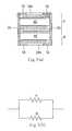
FIGS. 3a and 3 b are a side view of the electrical apparatus of multi-layers (2 layers) according to another preferred embodiment of the present invention and a schematic diagram of its equivalent electrical circuit.
PREFERRED EMBODIMENT OF THE PRESENT INVENTION
A surface mounted thermal-sensitive resistance apparatus according to a preferred embodiment of the present invention is illustrated by FIG. 1 to FIG. 3. Firstly, FIG. 1 is a side view of the electrical apparatus according to a preferred embodiment of the present invention, and the electrical apparatus shown in FIG. 1 mainly comprises a thin-board resistive component 10, first and second insulating films 14 a and 14 b, first and second conductive components 12 a and 12 b, and outer electrodes 16 and 18 coupled to the conductive films 20 and 22 respectively.
The resistive component 10 is made of a polymer material with conductive particles dispersed therein and having a characteristic of a positive or negative temperature coefficient. Polymeric materials suitable for the resistive component of the present invention comprises: polyethylene, polypropylene, polyvinyl fluoride, compound and copolymer of the materials mentioned above. The conductive particle can be a metal particle, carbon particle, metal oxide, metal carbide and compounds of the materials mentioned above.
On the top and bottom surfaces of the resistive component 10, the first and second conductive components 12 a and 12 b extend respectively to both corresponding sides. Two asymmetric indentations (one indentation is generated by stripping a metal film) are formed on the left side of the first conductive component and the other indentation is on the right side of the second conductive component by an ordinary etching method (such as laser trimming, chemical etching or mechanical method) from a planar metal foil, as shown in FIGS. 2(a) and 2(b). Materials of the conductive components could be nickel, copper, zinc, silver, gold, tin, lead, alloy and laminated material formed by the materials mentioned above. Besides, although the shape of the indentation in this embodiment is rectangular, other shapes, such as semi-circular, triangular, can also be used in the present invention. According to experiments, the area of the indentation is preferably less than 25% of the total area of one surface of the conductive component.
When the shape of the indentation after stripping is formed, any kind of excellent adhesive films 14 a and 14 b (such as an adhesive material made of epoxy and glass fiber, or further comprising polyimide, phenolic and polyester film) is used to adhere through heat and pressure between the resistive component and copper films on the upside and underside thereof. Afterward, both symmetrical electrodes 16 and 18 on the left and right ends are coated and formed by etching the center area of copper films.
The electrodes on the right and left ends 16 and 18 can be optionally electrically connected through interconnection vias 13 and 15 by electroplating, conductive materials on cross sectional end surfaces. Afterward, the intermediate region between the electrodes is coated with solder mask 24 a and 24 b to create an insulating effect.
In FIG. 1, the conductive film 20 inside the interconnection via 13 is coupled to two metal foils 16 and the first conductive component 12 a; and the conductive film 22 inside the interconnection via 15 is coupled to two metal foils 18 and the second conductive component 12 b. The wall of the interconnection vias can be electroplated with a layer of conductive metal (such as copper, gold, tin, alloy made from tin and lead) by electroless plating and electroplating methods to achieve the purpose of connecting the upper with lower electrodes. The cross-section shape of the interconnection vias could be circular, semi-circular, ¼ circular, arcuate, triangular, rectangular, rhombus or polygon. A semi-circular shape is used in this embodiment.
Referring to FIG. 3a, the number of resistive components is greater than or equal to two. In FIG. 3a, A and B represent two resistive components. The resistive component A is superimposed on the resistive component B, and they are electrically connected in parallel. Every conductive electrode component is electrically connected to others through interconnection vias embedded with conductive films 20 and 22. The surface mounted PTC apparatus according to the present invention has a length of 4.5 mm, a width of 3.1 mm and a thickness of 1.1 mm. Also, two PTC apparatuses are connected in parallel, and equivalent circuit of the PTC apparatuses connected in parallel is shown in FIG. 3b. An example of electrical characteristics of the PTC apparatus with two-layer design are listed in the following table.
The resistance after
Initial reflow process at 260° The resistance after cycle life tests.
resistance C. and mounted on a 1 10 100 500
(unit: Ω) circuit board (unit: Ω) cycle cycle cycle cycle
0.059 0.086 0.097 0.085 0.082 0.089
Cycle life test conditions are as follows:
Power source: 7 Volt DC, 40 Amp; 1 cycle: on time 6 sec and off time 60 sec.
The above-described embodiments of the present invention are intended to be illustrated only. Numerous alternative embodiments may be devised by those skilled in the art without departing, from the scope of the following claims.

Claims (20)

What is claimed is:
1. A surface mounted electrical apparatus, comprising:
(1) a thin-board resistive component, which is made of polymer material in which conductive particles are distributed, has a characteristic of positive or negative temperature coefficient, has opposite first and second surfaces, and has opposite first and second end surfaces, extending from the first surface to the second surface;
(2) a first conductive component, disposed on the first surface of said thin-board resistive component and extending to the first end surface;
(3) a second conductive component, disposed on the second surface of said thin-board resistive component and extending to the second end surface;
(4) a first insulating film, disposed on said first conductive component and extending to the second end surface of said thin-board resistive component;
(5) a second insulating film, disposed on said second conductive component and extending to the first end surface of said thin-board resistive component;
(6) a first electrode, including a main body and an interconnection via, wherein said main body includes a pair of metal foils disposed on said first and second insulating films, and said interconnection via includes a conductive film connected to said metal foils and said first conductive component along the first end surface; and
(7) a second electrode, including a main body and an interconnection via, wherein said main body includes a pair of metal foils disposed on said first and second insulating films, and said interconnection via includes a conductive film connected to said metal foils and said second conductive components along the second end surface. conductive components along the second end surface.
2. The electrical apparatus of claim 1, wherein said polymer material is selected from the group consisting polyethylene, polypropylene, polyvinyl fluoride, a mixture thereof or copolymer of the materials.
3. The electrical apparatus of claim 1, wherein said conductive particle is selected from the group consisting of metal particle, carbon particle, metal oxide, metal carbide and a mixture thereof.
4. The electrical apparatus of claim 1, wherein the conductive component is selected from the group consisting of nickel, copper, zinc, silver, gold, alloy of the materials and a laminated material made from the materials.
5. The electrical apparatus of claim 1, wherein said insulating film is an adhesive material.
6. The electrical apparatus of claim 5, wherein said insulating film is an adhesive material made of epoxy and glass fiber.
7. The electrical apparatus of claim 1, wherein said metal foil is copper foil.
8. The electrical apparatus of claim 1, wherein said conductive film is electroplated with copper or gold by an electroless plating or electroplating method.
9. The electrical apparatus of claim 1, further comprising:
(8) pair of isolating components, disposed respectively on said first and second insulating film for isolating the first electrode from second electrodes.
10. The electrical apparatus of claim 9, wherein said isolating component is a solder mask.
11. A surface mounted electrical apparatus, comprising:
(A) a first resistive assembly, including: (1) thin-board resistive components, each of said components has: (a) polymer materials in which conductive particles are distributed; (b) a characteristic of positive or negative temperature coefficient; (c) opposite first and second surfaces; (d) opposite first and second end surfaces, respectively extending from the first surface to the second surface; (2) a first conductive component, disposed on the first surface of said thin-board resistive component and extending to the first end surface; (3) a second conductive component, disposed on the second surface of said thin-board resistive components and extending to the second end surface; (4) a first insulating film, disposed on said first conductive component and extending to the second end surface of said thin-board resistance component; (5) a second insulating film disposed on the second conductive component and extending to the first end surface of said thin-board resistive component;
(B) at least one second resistive assembly of the same structure as said first resistive assembly and superimposed on said first resistive assembly;
(C) a first electrode, including a main body and an interconnection via, wherein said main body includes a pair of metal foils disposed on said first and second resistive assemblies and said interconnection via includes a conductive film coupled with said metal foils and said first conductive components along the first end surface; and
(D) a second electrode, including a main body and an interconnection via, wherein said main body includes a pair of metal foils disposed on said first and second resistive assemblies; said interconnection via includes a conductive film coupled as with said metal foils and said second conductive components along the second end surface.
12. The electrical apparatus of claim 11, wherein said polymer material is selected from the group consisting polyethylene, polypropylene, polyvinyl fluoride, a mixture thereof or copolymer of the materials.
13. The electrical apparatus of claim 11, wherein said conductive particle is selected from the croup consisting of metal particle, carbon particle, metal oxide, metal carbide and a mixture thereof.
14. The electrical apparatus of claim 11, wherein the conductive component is selected from the croup consisting of nickel, copper, zinc, silver, gold, alloy and a laminated material made from the materials.
15. The electrical apparatus of claim 11, wherein the insulating film is an adhesive material.
16. The electrical apparatus of claim 15, wherein the insulating film is an adhesive material made of epoxy and glass fiber.
17. The electrical apparatus of claim 11, wherein said metal foils are copper foils.
18. The electrical apparatus of claim 11, wherein the material of said conductive film is electroplated with copper, gold, tin or alloy made from tin and lead by an electroless plating or electroplating method.
19. The electrical apparatus of claim 11, further comprising:
(E) a pair of isolating components disposed on the first and second resistance assembly for isolating the first electrode from second electrode.
20. The electrical apparatus of claim 19, wherein said isolating component is a solder mask.
US09/542,283 1999-04-26 2000-04-04 Surface mountable over-current protecting device Expired - Lifetime US6377467B1 (en)

Applications Claiming Priority (2)

Application Number Priority Date Filing Date Title
TW088206474 1999-04-26
TW088206474U TW415624U (en) 1999-04-26 1999-04-26 Surface mounted electric apparatus

Publications (1)

Publication Number Publication Date
US6377467B1 true US6377467B1 (en) 2002-04-23

Family

ID=21647338

Family Applications (1)

Application Number Title Priority Date Filing Date
US09/542,283 Expired - Lifetime US6377467B1 (en) 1999-04-26 2000-04-04 Surface mountable over-current protecting device

Country Status (5)

Country Link
US (1) US6377467B1 (en)
JP (1) JP3073003U (en)
DE (1) DE20007462U1 (en)
FR (1) FR2792764B3 (en)
TW (1) TW415624U (en)

Cited By (29)

* Cited by examiner, † Cited by third party
Publication number Priority date Publication date Assignee Title
US20030099077A1 (en) * 2001-11-12 2003-05-29 Chu Edward Fu-Hua Multi-layer structure of a battery protection device
US20030227368A1 (en) * 2002-06-06 2003-12-11 Protectronics Technology Corporation Surface mountable laminated thermistor device
US6665164B2 (en) * 2001-03-20 2003-12-16 Polytronics Technology Corporation Surface mountable over-current protecting apparatus
US20040022001A1 (en) * 2002-07-31 2004-02-05 Chu Edward Fu-Hua Over-current protection device
WO2004053899A1 (en) * 2002-12-11 2004-06-24 Bourns, Inc. Conductive polymer device and method of manufacturing same
US6794980B2 (en) 2001-10-08 2004-09-21 Polytronics Technology Corporation Over-current protection apparatus and method for making the same
US20050141160A1 (en) * 2003-12-31 2005-06-30 Ma Yun C. Over-current protection apparatus
US20060055501A1 (en) * 2002-12-10 2006-03-16 Bourns., Inc Conductive polymer device and method of manufacturing same
US20060055500A1 (en) * 2002-12-11 2006-03-16 Bourns, Inc Encapsulated conductive polymer device and method of manufacturing the same
US20060269308A1 (en) * 2005-05-30 2006-11-30 Takeshi Ishii Temperature detector and fixing device provided therewith
WO2007121412A3 (en) * 2006-04-14 2008-06-19 Bourns Inc Conductive polymer electronic devices with surface mountable configuration and methods for manufacturing same
US20090027821A1 (en) * 2007-07-26 2009-01-29 Littelfuse, Inc. Integrated thermistor and metallic element device and method
US8421584B2 (en) 2011-01-17 2013-04-16 Polytronics Technology Corp. Over-current protection device and method for manufacturing the same
USRE44224E1 (en) * 2005-12-27 2013-05-21 Polytronics Technology Corp. Surface-mounted over-current protection device
US8502638B1 (en) * 2012-02-03 2013-08-06 Polytronics Technology Corp. Thermistor
US8525636B1 (en) * 2012-04-04 2013-09-03 Polytronics Technology Corp. Thermistor
KR20140067107A (en) 2011-09-15 2014-06-03 타이코 일렉트로닉스 저팬 지.케이. Positive temperature coefficient(ptc) device
US20140285938A1 (en) * 2013-03-22 2014-09-25 Polytronics Technology Corp. Over-current protection device
CN104218553A (en) * 2013-05-31 2014-12-17 聚鼎科技股份有限公司 Overcurrent protection assembly capable of inhibiting surge
CN104319044A (en) * 2014-10-25 2015-01-28 广东风华高新科技股份有限公司 Thermal-pressure sensitive device packaging structure and thermal-pressure sensitive device
US9000881B2 (en) 2012-09-06 2015-04-07 Polytronics Technology Corp. Surface mountable over-current protection device
US9142949B2 (en) 2011-07-29 2015-09-22 Tyco Electronics Japan G.K. PTC device
CN105280316A (en) * 2015-09-26 2016-01-27 广东百圳君耀电子有限公司 Intelligent protection element and manufacturing technology therefor
US10096407B2 (en) 2016-07-29 2018-10-09 Polytronics Technology Corp. Surface-mountable over-current protection device
US10141089B1 (en) 2017-05-16 2018-11-27 Polytronics Technology Corp. Surface-mountable over-current protection device
EP3506325A1 (en) * 2017-12-21 2019-07-03 The Boeing Company Multilayer stack comprising conductive polymer layers with enhanced conductivity and stability and fabrication method therefor
US10614935B1 (en) 2018-09-27 2020-04-07 Polytronics Technology Corp. PTC device
US10892072B1 (en) 2019-08-15 2021-01-12 Polytronics Technology Corp. PTC device
DE102022126526A1 (en) 2022-10-12 2024-04-18 Tdk Electronics Ag Sensor element and method for producing a sensor element

Families Citing this family (6)

* Cited by examiner, † Cited by third party
Publication number Priority date Publication date Assignee Title
JP2002313604A (en) * 2001-04-18 2002-10-25 Tdk Corp Polymer ptc device
US7708912B2 (en) * 2008-06-16 2010-05-04 Polytronics Technology Corporation Variable impedance composition
DE102008017269A1 (en) * 2008-04-04 2009-10-15 Epcos Ag Positive temperature coefficient resistor element, has two edge layers arranged on base body, where specific resistance of edge layers is greater than specific resistance of base body
CN103106988B (en) * 2011-11-11 2015-10-14 聚鼎科技股份有限公司 Thermistor element
EP3351439B1 (en) 2017-01-24 2019-11-20 Valeo Systèmes d'Essuyage Wiper blade comprising an electrical heating circuit and a ptc fuse
US11650391B2 (en) * 2020-02-25 2023-05-16 Littelfuse, Inc. PPTC heater and material having stable power and self-limiting behavior

Citations (10)

* Cited by examiner, † Cited by third party
Publication number Priority date Publication date Assignee Title
US5025271A (en) * 1986-07-01 1991-06-18 Hewlett-Packard Company Thin film resistor type thermal ink pen using a form storage ink supply
US5089801A (en) 1990-09-28 1992-02-18 Raychem Corporation Self-regulating ptc devices having shaped laminar conductive terminals
US5699607A (en) * 1996-01-22 1997-12-23 Littelfuse, Inc. Process for manufacturing an electrical device comprising a PTC element
US5831510A (en) 1994-05-16 1998-11-03 Zhang; Michael PTC electrical devices for installation on printed circuit boards
US5852397A (en) 1992-07-09 1998-12-22 Raychem Corporation Electrical devices
US5864281A (en) 1994-06-09 1999-01-26 Raychem Corporation Electrical devices containing a conductive polymer element having a fractured surface
US5876842A (en) * 1995-06-07 1999-03-02 International Business Machines Corporation Modular circuit package having vertically aligned power and signal cores
US5884391A (en) * 1996-01-22 1999-03-23 Littelfuse, Inc. Process for manufacturing an electrical device comprising a PTC element
US5900800A (en) * 1996-01-22 1999-05-04 Littelfuse, Inc. Surface mountable electrical device comprising a PTC element
US6023403A (en) 1996-05-03 2000-02-08 Littlefuse, Inc. Surface mountable electrical device comprising a PTC and fusible element

Patent Citations (10)

* Cited by examiner, † Cited by third party
Publication number Priority date Publication date Assignee Title
US5025271A (en) * 1986-07-01 1991-06-18 Hewlett-Packard Company Thin film resistor type thermal ink pen using a form storage ink supply
US5089801A (en) 1990-09-28 1992-02-18 Raychem Corporation Self-regulating ptc devices having shaped laminar conductive terminals
US5852397A (en) 1992-07-09 1998-12-22 Raychem Corporation Electrical devices
US5831510A (en) 1994-05-16 1998-11-03 Zhang; Michael PTC electrical devices for installation on printed circuit boards
US5864281A (en) 1994-06-09 1999-01-26 Raychem Corporation Electrical devices containing a conductive polymer element having a fractured surface
US5876842A (en) * 1995-06-07 1999-03-02 International Business Machines Corporation Modular circuit package having vertically aligned power and signal cores
US5699607A (en) * 1996-01-22 1997-12-23 Littelfuse, Inc. Process for manufacturing an electrical device comprising a PTC element
US5884391A (en) * 1996-01-22 1999-03-23 Littelfuse, Inc. Process for manufacturing an electrical device comprising a PTC element
US5900800A (en) * 1996-01-22 1999-05-04 Littelfuse, Inc. Surface mountable electrical device comprising a PTC element
US6023403A (en) 1996-05-03 2000-02-08 Littlefuse, Inc. Surface mountable electrical device comprising a PTC and fusible element

Cited By (49)

* Cited by examiner, † Cited by third party
Publication number Priority date Publication date Assignee Title
US6665164B2 (en) * 2001-03-20 2003-12-16 Polytronics Technology Corporation Surface mountable over-current protecting apparatus
US6794980B2 (en) 2001-10-08 2004-09-21 Polytronics Technology Corporation Over-current protection apparatus and method for making the same
US20030099077A1 (en) * 2001-11-12 2003-05-29 Chu Edward Fu-Hua Multi-layer structure of a battery protection device
US20030227368A1 (en) * 2002-06-06 2003-12-11 Protectronics Technology Corporation Surface mountable laminated thermistor device
US6873244B2 (en) * 2002-06-06 2005-03-29 Protectronics Technology Corporation Surface mountable laminated thermistor device
US20040022001A1 (en) * 2002-07-31 2004-02-05 Chu Edward Fu-Hua Over-current protection device
US6809626B2 (en) 2002-07-31 2004-10-26 Polytronics Technology Corporation Over-current protection device
US20060055501A1 (en) * 2002-12-10 2006-03-16 Bourns., Inc Conductive polymer device and method of manufacturing same
US20060152329A1 (en) * 2002-12-11 2006-07-13 Sten Bjorsell Conductive polymer device and method of manufacturing same
US20060055500A1 (en) * 2002-12-11 2006-03-16 Bourns, Inc Encapsulated conductive polymer device and method of manufacturing the same
WO2004053899A1 (en) * 2002-12-11 2004-06-24 Bourns, Inc. Conductive polymer device and method of manufacturing same
US20050141160A1 (en) * 2003-12-31 2005-06-30 Ma Yun C. Over-current protection apparatus
US7071810B2 (en) 2003-12-31 2006-07-04 Polytronics Technology Corporation Over-current protection apparatus
US7538654B2 (en) * 2005-05-30 2009-05-26 Kyocera Mita Corporation Temperature detector and fixing device provided therewith
US20060269308A1 (en) * 2005-05-30 2006-11-30 Takeshi Ishii Temperature detector and fixing device provided therewith
USRE44224E1 (en) * 2005-12-27 2013-05-21 Polytronics Technology Corp. Surface-mounted over-current protection device
US8542086B2 (en) 2006-04-14 2013-09-24 Bourns, Inc. Conductive polymer electronic devices with surface mountable configuration and methods for manufacturing same
EP2014143A4 (en) * 2006-04-14 2015-03-11 Bourns Inc Conductive polymer electronic devices with surface mountable configuration and methods for manufacturing same
US20110175700A1 (en) * 2006-04-14 2011-07-21 Bourns, Inc. Conductive polymer electronic devices with surface mountable configuration and methods for manufacturing same
EP2014143A2 (en) * 2006-04-14 2009-01-14 Bourns, Inc. Conductive polymer electronic devices with surface mountable configuration and methods for manufacturing same
US9552909B2 (en) 2006-04-14 2017-01-24 Bourns, Inc. Conductive polymer electronic devices with surface mountable configuration and methods for manufacturing same
US9697934B2 (en) 2006-04-14 2017-07-04 Bourns, Inc. Conductive polymer electronic devices with surface mountable configuration and methods for manufacturing same
WO2007121412A3 (en) * 2006-04-14 2008-06-19 Bourns Inc Conductive polymer electronic devices with surface mountable configuration and methods for manufacturing same
TWI427646B (en) * 2006-04-14 2014-02-21 Bourns Inc Conductive polymer electronic devices with surface mountable configuration and methods for manufacturing same
US20090027821A1 (en) * 2007-07-26 2009-01-29 Littelfuse, Inc. Integrated thermistor and metallic element device and method
US8421584B2 (en) 2011-01-17 2013-04-16 Polytronics Technology Corp. Over-current protection device and method for manufacturing the same
US9142949B2 (en) 2011-07-29 2015-09-22 Tyco Electronics Japan G.K. PTC device
KR20140067107A (en) 2011-09-15 2014-06-03 타이코 일렉트로닉스 저팬 지.케이. Positive temperature coefficient(ptc) device
US20130200987A1 (en) * 2012-02-03 2013-08-08 Polytronics Technology Corp. Thermistor
US8502638B1 (en) * 2012-02-03 2013-08-06 Polytronics Technology Corp. Thermistor
US8525636B1 (en) * 2012-04-04 2013-09-03 Polytronics Technology Corp. Thermistor
US9000881B2 (en) 2012-09-06 2015-04-07 Polytronics Technology Corp. Surface mountable over-current protection device
US20140285938A1 (en) * 2013-03-22 2014-09-25 Polytronics Technology Corp. Over-current protection device
US9401234B2 (en) * 2013-03-22 2016-07-26 Polytronics Technology Corp. Over-current protection device
CN104218553A (en) * 2013-05-31 2014-12-17 聚鼎科技股份有限公司 Overcurrent protection assembly capable of inhibiting surge
CN104218553B (en) * 2013-05-31 2017-04-19 聚鼎科技股份有限公司 Overcurrent protection assembly capable of inhibiting surge
CN104319044A (en) * 2014-10-25 2015-01-28 广东风华高新科技股份有限公司 Thermal-pressure sensitive device packaging structure and thermal-pressure sensitive device
CN105280316A (en) * 2015-09-26 2016-01-27 广东百圳君耀电子有限公司 Intelligent protection element and manufacturing technology therefor
CN105280316B (en) * 2015-09-26 2018-05-11 广东百圳君耀电子有限公司 The element of intelligent protection and technique is made
US10096407B2 (en) 2016-07-29 2018-10-09 Polytronics Technology Corp. Surface-mountable over-current protection device
US10141089B1 (en) 2017-05-16 2018-11-27 Polytronics Technology Corp. Surface-mountable over-current protection device
EP3506325A1 (en) * 2017-12-21 2019-07-03 The Boeing Company Multilayer stack comprising conductive polymer layers with enhanced conductivity and stability and fabrication method therefor
CN110033911A (en) * 2017-12-21 2019-07-19 波音公司 Multiple-level stack with enhancing conductivity and stability
US10541065B2 (en) * 2017-12-21 2020-01-21 The Boeing Company Multilayer stack with enhanced conductivity and stability
US10607747B1 (en) * 2017-12-21 2020-03-31 The Boeing Company Multilayer stack with enhanced conductivity and stability
CN110033911B (en) * 2017-12-21 2022-10-25 波音公司 Multilayer stack with enhanced conductivity and stability
US10614935B1 (en) 2018-09-27 2020-04-07 Polytronics Technology Corp. PTC device
US10892072B1 (en) 2019-08-15 2021-01-12 Polytronics Technology Corp. PTC device
DE102022126526A1 (en) 2022-10-12 2024-04-18 Tdk Electronics Ag Sensor element and method for producing a sensor element

Also Published As

Publication number Publication date
FR2792764B3 (en) 2001-04-13
TW415624U (en) 2000-12-11
JP3073003U (en) 2000-11-14
FR2792764A3 (en) 2000-10-27
DE20007462U1 (en) 2000-11-30

Similar Documents

Publication Publication Date Title
US6377467B1 (en) Surface mountable over-current protecting device
US6108184A (en) Surface mountable electrical device comprising a voltage variable material
JP5259289B2 (en) Integrated thermistor, metal element device and method
US7180719B2 (en) Integrated overvoltage and overcurrent device
US8842406B2 (en) Over-current protection device
KR20030061353A (en) Low resistance polymer matrix fuse apparatus and method
JPH11162708A (en) Multi-layered conductive polymer positive temperature coefficient device
JP2010015976A (en) Circuit protection device including resistor and fuse element
EP0232868B1 (en) Fused solid electrolytic capacitor
US6838972B1 (en) PTC circuit protection devices
US20020125982A1 (en) Surface mount electrical device with multiple ptc elements
TWI230453B (en) Over-current protection device and manufacturing method thereof
JP3736602B2 (en) Chip type thermistor
TWI441200B (en) Surface mountable over-current protection device
US8803653B2 (en) Over-current protection device
KR100685088B1 (en) Surface-mounting type thermistor having multi layers and method of manufacturing the same
CN111696738B (en) Overcurrent protection element
US7071810B2 (en) Over-current protection apparatus
TWI493576B (en) Over-current protection device and protective curcuit board containing the same
KR19990081968A (en) Surface-Mounted Electrical Equipment Including PTC Element
US7205878B2 (en) Over-current protection device and manufacturing method thereof
CN108878080B (en) Surface adhesive overcurrent protection element
KR100505475B1 (en) PTC thermistor having electrodes on the same surface and method thereof
TW463443B (en) A PTC circuit protection device
KR100496450B1 (en) Surface mountable electrical device for printed circuit board and method of manufacturing the same

Legal Events

Date Code Title Description
AS Assignment

Owner name: POLYTRONICS TECHNOLOGY CORPORATION, TAIWAN

Free format text: ASSIGNMENT OF ASSIGNORS INTEREST;ASSIGNORS:CHU, FU-HUA;MA, YUN-CHING;WANG, DAVID SHAU-CHEW;REEL/FRAME:010757/0331;SIGNING DATES FROM 20000313 TO 20000314

FEPP Fee payment procedure

Free format text: PAYOR NUMBER ASSIGNED (ORIGINAL EVENT CODE: ASPN); ENTITY STATUS OF PATENT OWNER: LARGE ENTITY

STCF Information on status: patent grant

Free format text: PATENTED CASE

FEPP Fee payment procedure

Free format text: PAYER NUMBER DE-ASSIGNED (ORIGINAL EVENT CODE: RMPN); ENTITY STATUS OF PATENT OWNER: LARGE ENTITY

FPAY Fee payment

Year of fee payment: 4

FPAY Fee payment

Year of fee payment: 8

FEPP Fee payment procedure

Free format text: PAT HOLDER NO LONGER CLAIMS SMALL ENTITY STATUS, ENTITY STATUS SET TO UNDISCOUNTED (ORIGINAL EVENT CODE: STOL); ENTITY STATUS OF PATENT OWNER: LARGE ENTITY

FPAY Fee payment

Year of fee payment: 12