US6369331B1 - Printed circuit board for semiconductor package and method of making same - Google Patents
Printed circuit board for semiconductor package and method of making same Download PDFInfo
- Publication number
- US6369331B1 US6369331B1 US09/536,992 US53699200A US6369331B1 US 6369331 B1 US6369331 B1 US 6369331B1 US 53699200 A US53699200 A US 53699200A US 6369331 B1 US6369331 B1 US 6369331B1
- Authority
- US
- United States
- Prior art keywords
- substrate
- front surface
- back surface
- wiring pattern
- circuit board
- Prior art date
- Legal status (The legal status is an assumption and is not a legal conclusion. Google has not performed a legal analysis and makes no representation as to the accuracy of the status listed.)
- Expired - Fee Related
Links
Images


Classifications
-
- H—ELECTRICITY
- H01—ELECTRIC ELEMENTS
- H01L—SEMICONDUCTOR DEVICES NOT COVERED BY CLASS H10
- H01L23/00—Details of semiconductor or other solid state devices
- H01L23/48—Arrangements for conducting electric current to or from the solid state body in operation, e.g. leads, terminal arrangements ; Selection of materials therefor
- H01L23/488—Arrangements for conducting electric current to or from the solid state body in operation, e.g. leads, terminal arrangements ; Selection of materials therefor consisting of soldered or bonded constructions
- H01L23/498—Leads, i.e. metallisations or lead-frames on insulating substrates, e.g. chip carriers
- H01L23/4985—Flexible insulating substrates
-
- H—ELECTRICITY
- H01—ELECTRIC ELEMENTS
- H01L—SEMICONDUCTOR DEVICES NOT COVERED BY CLASS H10
- H01L23/00—Details of semiconductor or other solid state devices
- H01L23/48—Arrangements for conducting electric current to or from the solid state body in operation, e.g. leads, terminal arrangements ; Selection of materials therefor
- H01L23/488—Arrangements for conducting electric current to or from the solid state body in operation, e.g. leads, terminal arrangements ; Selection of materials therefor consisting of soldered or bonded constructions
- H01L23/498—Leads, i.e. metallisations or lead-frames on insulating substrates, e.g. chip carriers
- H01L23/49811—Additional leads joined to the metallisation on the insulating substrate, e.g. pins, bumps, wires, flat leads
- H01L23/49816—Spherical bumps on the substrate for external connection, e.g. ball grid arrays [BGA]
-
- H—ELECTRICITY
- H01—ELECTRIC ELEMENTS
- H01L—SEMICONDUCTOR DEVICES NOT COVERED BY CLASS H10
- H01L2224/00—Indexing scheme for arrangements for connecting or disconnecting semiconductor or solid-state bodies and methods related thereto as covered by H01L24/00
- H01L2224/01—Means for bonding being attached to, or being formed on, the surface to be connected, e.g. chip-to-package, die-attach, "first-level" interconnects; Manufacturing methods related thereto
- H01L2224/42—Wire connectors; Manufacturing methods related thereto
- H01L2224/44—Structure, shape, material or disposition of the wire connectors prior to the connecting process
- H01L2224/45—Structure, shape, material or disposition of the wire connectors prior to the connecting process of an individual wire connector
- H01L2224/45001—Core members of the connector
- H01L2224/4501—Shape
- H01L2224/45012—Cross-sectional shape
- H01L2224/45014—Ribbon connectors, e.g. rectangular cross-section
-
- H—ELECTRICITY
- H01—ELECTRIC ELEMENTS
- H01L—SEMICONDUCTOR DEVICES NOT COVERED BY CLASS H10
- H01L2224/00—Indexing scheme for arrangements for connecting or disconnecting semiconductor or solid-state bodies and methods related thereto as covered by H01L24/00
- H01L2224/01—Means for bonding being attached to, or being formed on, the surface to be connected, e.g. chip-to-package, die-attach, "first-level" interconnects; Manufacturing methods related thereto
- H01L2224/42—Wire connectors; Manufacturing methods related thereto
- H01L2224/44—Structure, shape, material or disposition of the wire connectors prior to the connecting process
- H01L2224/45—Structure, shape, material or disposition of the wire connectors prior to the connecting process of an individual wire connector
- H01L2224/45001—Core members of the connector
- H01L2224/45099—Material
- H01L2224/451—Material with a principal constituent of the material being a metal or a metalloid, e.g. boron (B), silicon (Si), germanium (Ge), arsenic (As), antimony (Sb), tellurium (Te) and polonium (Po), and alloys thereof
- H01L2224/45138—Material with a principal constituent of the material being a metal or a metalloid, e.g. boron (B), silicon (Si), germanium (Ge), arsenic (As), antimony (Sb), tellurium (Te) and polonium (Po), and alloys thereof the principal constituent melting at a temperature of greater than or equal to 950°C and less than 1550°C
- H01L2224/45144—Gold (Au) as principal constituent
-
- H—ELECTRICITY
- H01—ELECTRIC ELEMENTS
- H01L—SEMICONDUCTOR DEVICES NOT COVERED BY CLASS H10
- H01L2224/00—Indexing scheme for arrangements for connecting or disconnecting semiconductor or solid-state bodies and methods related thereto as covered by H01L24/00
- H01L2224/01—Means for bonding being attached to, or being formed on, the surface to be connected, e.g. chip-to-package, die-attach, "first-level" interconnects; Manufacturing methods related thereto
- H01L2224/42—Wire connectors; Manufacturing methods related thereto
- H01L2224/47—Structure, shape, material or disposition of the wire connectors after the connecting process
- H01L2224/48—Structure, shape, material or disposition of the wire connectors after the connecting process of an individual wire connector
- H01L2224/4805—Shape
- H01L2224/4809—Loop shape
- H01L2224/48091—Arched
-
- H—ELECTRICITY
- H01—ELECTRIC ELEMENTS
- H01L—SEMICONDUCTOR DEVICES NOT COVERED BY CLASS H10
- H01L2224/00—Indexing scheme for arrangements for connecting or disconnecting semiconductor or solid-state bodies and methods related thereto as covered by H01L24/00
- H01L2224/01—Means for bonding being attached to, or being formed on, the surface to be connected, e.g. chip-to-package, die-attach, "first-level" interconnects; Manufacturing methods related thereto
- H01L2224/42—Wire connectors; Manufacturing methods related thereto
- H01L2224/47—Structure, shape, material or disposition of the wire connectors after the connecting process
- H01L2224/48—Structure, shape, material or disposition of the wire connectors after the connecting process of an individual wire connector
- H01L2224/481—Disposition
- H01L2224/48151—Connecting between a semiconductor or solid-state body and an item not being a semiconductor or solid-state body, e.g. chip-to-substrate, chip-to-passive
- H01L2224/48221—Connecting between a semiconductor or solid-state body and an item not being a semiconductor or solid-state body, e.g. chip-to-substrate, chip-to-passive the body and the item being stacked
- H01L2224/48225—Connecting between a semiconductor or solid-state body and an item not being a semiconductor or solid-state body, e.g. chip-to-substrate, chip-to-passive the body and the item being stacked the item being non-metallic, e.g. insulating substrate with or without metallisation
- H01L2224/48227—Connecting between a semiconductor or solid-state body and an item not being a semiconductor or solid-state body, e.g. chip-to-substrate, chip-to-passive the body and the item being stacked the item being non-metallic, e.g. insulating substrate with or without metallisation connecting the wire to a bond pad of the item
-
- H—ELECTRICITY
- H01—ELECTRIC ELEMENTS
- H01L—SEMICONDUCTOR DEVICES NOT COVERED BY CLASS H10
- H01L24/00—Arrangements for connecting or disconnecting semiconductor or solid-state bodies; Methods or apparatus related thereto
- H01L24/01—Means for bonding being attached to, or being formed on, the surface to be connected, e.g. chip-to-package, die-attach, "first-level" interconnects; Manufacturing methods related thereto
- H01L24/42—Wire connectors; Manufacturing methods related thereto
- H01L24/44—Structure, shape, material or disposition of the wire connectors prior to the connecting process
- H01L24/45—Structure, shape, material or disposition of the wire connectors prior to the connecting process of an individual wire connector
-
- H—ELECTRICITY
- H01—ELECTRIC ELEMENTS
- H01L—SEMICONDUCTOR DEVICES NOT COVERED BY CLASS H10
- H01L24/00—Arrangements for connecting or disconnecting semiconductor or solid-state bodies; Methods or apparatus related thereto
- H01L24/01—Means for bonding being attached to, or being formed on, the surface to be connected, e.g. chip-to-package, die-attach, "first-level" interconnects; Manufacturing methods related thereto
- H01L24/42—Wire connectors; Manufacturing methods related thereto
- H01L24/47—Structure, shape, material or disposition of the wire connectors after the connecting process
- H01L24/48—Structure, shape, material or disposition of the wire connectors after the connecting process of an individual wire connector
-
- H—ELECTRICITY
- H01—ELECTRIC ELEMENTS
- H01L—SEMICONDUCTOR DEVICES NOT COVERED BY CLASS H10
- H01L2924/00—Indexing scheme for arrangements or methods for connecting or disconnecting semiconductor or solid-state bodies as covered by H01L24/00
- H01L2924/0001—Technical content checked by a classifier
- H01L2924/00014—Technical content checked by a classifier the subject-matter covered by the group, the symbol of which is combined with the symbol of this group, being disclosed without further technical details
-
- H—ELECTRICITY
- H01—ELECTRIC ELEMENTS
- H01L—SEMICONDUCTOR DEVICES NOT COVERED BY CLASS H10
- H01L2924/00—Indexing scheme for arrangements or methods for connecting or disconnecting semiconductor or solid-state bodies as covered by H01L24/00
- H01L2924/01—Chemical elements
- H01L2924/01079—Gold [Au]
-
- H—ELECTRICITY
- H01—ELECTRIC ELEMENTS
- H01L—SEMICONDUCTOR DEVICES NOT COVERED BY CLASS H10
- H01L2924/00—Indexing scheme for arrangements or methods for connecting or disconnecting semiconductor or solid-state bodies as covered by H01L24/00
- H01L2924/15—Details of package parts other than the semiconductor or other solid state devices to be connected
- H01L2924/151—Die mounting substrate
- H01L2924/153—Connection portion
- H01L2924/1531—Connection portion the connection portion being formed only on the surface of the substrate opposite to the die mounting surface
- H01L2924/15311—Connection portion the connection portion being formed only on the surface of the substrate opposite to the die mounting surface being a ball array, e.g. BGA
-
- H—ELECTRICITY
- H01—ELECTRIC ELEMENTS
- H01L—SEMICONDUCTOR DEVICES NOT COVERED BY CLASS H10
- H01L2924/00—Indexing scheme for arrangements or methods for connecting or disconnecting semiconductor or solid-state bodies as covered by H01L24/00
- H01L2924/15—Details of package parts other than the semiconductor or other solid state devices to be connected
- H01L2924/181—Encapsulation
Definitions
- the present invention relates to a semiconductor package such as a ball grid array (BGA), in particular, to a printed circuit board employed in such a semiconductor package.
- BGA ball grid array
- a BGA employs conductive through holes or vias so as to electrically connect a semiconductor chip, mounted on the front surface of a substrate, and solder balls attached to the back surface of the substrate.
- An increased number of input/output pins arranged on the semiconductor chip inevitably induces increased through holes.
- the increase of the through holes may hinder realization of a high-density and fine printed wiring pattern on the substrate.
- production efficiency may be deteriorated and cost in production may be increased.
- Japanese Patent Laid-open No. 8-31868 discloses a semiconductor package, a BGA, comprising a semiconductor chip and solder balls electrically connected to each other without employment of through holes.
- the disclosed BGA is designed to employ a printed circuit board comprising a folded insulated film of synthetic resin. A printed wiring pattern is formed over the surface of the insulated film. Electric connection can thus be achieved between the semiconductor chip and the solder balls via the printed circuit pattern, not through holes, in the BGA.
- the BGA may suffer from an insufficient rigidity of the printed circuit board. Stress applied to the BGA may induce deformation of the semiconductor chip, which possibly disconnects the electric connection between the semiconductor chip and the printed circuit board.
- FIG. 8-204103 Another example of a BGA is disclosed in Japanese Patent Laid-open No. 8-204103.
- This BGA tries to maintain the rigidity of a printed circuit board even when a semiconductor chip and solder balls are electrically connected to each other without employment of through holes.
- the BGA is designed to employ a multilayered printed circuit board comprising a metallic plate, an insulator layer and a printed pattern film.
- the metallic plate serves to exhibit a higher rigidity.
- folding of the high rigidity metallic plate may deteriorate production efficiency.
- a printed circuit board for a semiconductor package comprising: a substrate having a front surface and a back surface; an insulator film extending over the front surface and bent around an outer periphery of the front surface so as to reach the back surface; and a wiring pattern printed on the insulator film so as to extend over the front and back surfaces.
- the wiring pattern serves to electrically connect the opposite surfaces, namely, the front and back surfaces of the printed circuit board. Employment of such a wiring pattern allows establishment of signal paths between the front and back surfaces of the printed circuit board without a conductive through hole or via.
- the wiring pattern may serve to facilitate establishment of electric connection between a semiconductor chip, mounted on the front surface of the printed circuit board, and a plurality of conductive balls such as solder balls and gold balls, formed or attached to the back surface of the printed circuit board. It is not required to form conductive through holes or vias. Even if input/output pins of the semiconductor chip are increased, it is possible to avoid a deteriorated efficiency and an increased cost in production.
- a rigid body is preferably employed as a substrate.
- a rigid body may include a conventional resin plate, a copper plate, an aluminum plate, a ceramic plate, and the like, for example.
- the semiconductor package is reliably prevented from deformation.
- the semiconductor package can be grasped relatively hard.
- a wire bonding can be achieved easily.
- the printed circuit board preferably further comprises a lining of a metallic thin film backing the insulator film.
- the metallic thin film may contribute to reinforcement of rigidity of the insulator film. If the synthetic resin insulator film is formed on the surface of the metallic thin film, the metallic thin film along with the insulator film can be rolled up onto a roll. Handling of the relatively fragile insulator film can be facilitated. It is preferable to keep enough flexibility in the metallic thin film even after the insulator film or membrane is coated on the surface of the metallic thin film.
- a metallic plate of a higher heat conduction when employed as the substrate, it is preferable to define an opening in the insulator film and/or the metallic thin film so as to expose the front surface of the metallic plate. If the semiconductor chip is disposed within the opening so as to directly contact the metallic plate, heat radiation from the semiconductor chip can be promoted through the heat conduction of the metallic plate. A heat sink, a heat pipe, or any other type of heat radiation mechanism may be added or attached to the metallic plate.
- the conductive metallic thin film may be utilized as a ground pattern or layer. If the wiring pattern is connected to the ground pattern, a structure similar to a micro strip line can easily be established, so that a signal line can be prevented from suffering from noise crossing over adjacent signal lines.
- a method according to the invention may comprise: forming an insulator membrane on a front surface of a film; forming a conductive wiring pattern on a surface of the insulator membrane; attaching a core on a back surface of the film; folding a part of the film around an outer periphery of the core; and bonding the part at a back of the core, for example.
- the core may include a metallic plate such as a copper plate and an aluminum plate in addition to a substrate such as a synthetic resin plate and a ceramic plate.
- the core need not be a rigid body in this case.
- the film may take the form of ribbon.
- the film in the form of ribbon may be rolled up onto a roll after the conductive wiring pattern has been formed. Employment of the roll serves to facilitate handling of the film at factories.
- FIG. 1 is a side view schematically illustrating the structure of a ball grid array (BGA) according to a first embodiment of the present invention
- FIG. 2 schematically illustrates a method of making a printed circuit board employed in the BGA
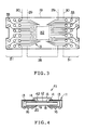
- FIG. 3 is a plan view of a metallic thin film for illustrating a printed wiring pattern
- FIG. 4 is a side view schematically illustrating the structure of a BGA according to a second embodiment of the present invention.
- FIG. 5 illustrates a plan view of a metallic thin film for realizing the BGA of the second embodiment
- FIG. 6 is a side view illustrating the structure of a BGA in which a heat sink is attached to a metallic plate.
- FIG. 7 is an enlarged sectional view partly illustrating the printed circuit board comprising a micro strip line.
- FIG. 1 schematically illustrates a semiconductor package according to a first embodiment of the present invention.
- the semiconductor package or ball grid array (BGA) 10 comprises a printed circuit board 11 and a semiconductor chip 12 mounted on the front or upper surface of the printed circuit board 11 .
- a conductive printed pattern or wiring pattern 13 extends over the front surface of the printed circuit board 11 .
- Gold wires 14 are designed to electrically connect input/output terminals of the semiconductor chip 12 and corresponding portions or input/output pads of the wiring pattern 13 .
- the semiconductor chip 12 and the gold wires 14 are sealed within a hardened resin 15 .
- a plurality of solder balls 16 are attached to the back or lower surface of the printed circuit board 11 .
- the solder balls 16 may be arranged in a lattice pattern, for example.
- the respective input/output terminals of the semiconductor chip 12 are electrically connected to the corresponding solder balls 16 through wires included in the wiring pattern 13 , as described later in detail.
- MCM multi-chip module
- the solder balls 16 are designed to melt on input/output pads arranged on the printed circuit board.
- the solder balls 16 are thereafter caused to harden by a cooling treatment.
- the hardened solder balls 16 serve to fixedly hold the BGA 10 on the input/output pads. In this manner, an electric connection can be achieved between the semiconductor chip 12 in the BGA 10 and the printed circuit board in the MCM or motherboard.
- the printed circuit board 11 comprises a metallic plate 18 as a core or substrate, and a flexible metallic thin film 19 extending over the front or upper surface of the metallic plate 18 .
- the metallic thin film 19 is designed to bend around the outer periphery of the metallic plate 18 so as to reach the back or lower surface of the metallic plate 18 .
- a flexible insulator film or membrane 20 is layered over the surface of the metallic thin film 19 .
- the metallic thin film 19 thus functions as a lining backing the insulator membrane 20 .
- the aforementioned wiring pattern 13 is formed to extend over the surface of the insulator membrane 20 .
- the wiring pattern 13 thus extends over both the opposite surfaces, namely, the front and back surfaces around the outer periphery of the metallic plate 18 .
- the core or substrate may include not only the aforementioned metallic plate 18 such as a copper plate and an aluminum plate but also a synthetic resin plate or a ceramic plate.
- the core or substrate is preferably designed to have a rigidity enough to avoid deformation when stress is applied to the core or substrate. Enough rigidity can be achieved, for example, in a copper or an aluminum plate of approximately 0.5 mm to 1.0 mm thickness.
- the metallic thin film 19 may include a stainless steel thin film, for example.
- the insulator film or membrane 20 may include a flexible synthetic resin coating, for example.
- the wiring pattern 13 is adapted to establish an electric connection between the semiconductor chip 12 , on the front surface of the printed circuit board 11 , and the solder balls 16 on the back surface of the printed circuit board 11 , in the BGA 10 .
- a through hole is not required in the printed circuit board 11 . Even when an increased number of input/output pins are arranged on the semiconductor chip 12 , it is possible to avoid a deteriorated production efficiency and an increased production cost.
- a ribbon 23 of stainless steel rolled around a first roll 22 is prepared.
- the ribbon 23 may have a thickness of approximately 25 ⁇ m, for example.
- Liquid of photosensitive polyimide 24 is applied to the front surface of the ribbon 23 released from the first roll 22 .
- the insulator membrane or coating 20 can be obtained on the surface of the ribbon 23 .
- the insulator membrane 20 may have a thickness of approximately 40 ⁇ m, for example.
- a copper 25 is applied to the surface of the insulator membrane 20 .
- the wiring pattern 13 is thus printed and formed by the copper 25 .
- An electrodeposition may be employed to form the wiring pattern 13 . Since the ribbon 23 and the insulator membrane 20 have the aforementioned thickness, the ribbon 23 including the copper wiring pattern 13 has a flexibility enough to be rolled up onto a second roll 26 . Employment of the first and second rolls 22 , 26 serves to facilitate handling of the ribbon 23 at factories.
- the metallic thin film 19 is punched out of the ribbon 23 of stainless steel prepared in the above-described manner. As shown in FIG. 3, a main section 28 is then defined by a pair of fold lines 29 , 29 extending on the surface of the metallic thin film 19 . The main section 28 is expected to be superposed on the front surface of the metallic plate 18 . Likewise, a pair of bent sections 31 , 31 are defined by fold lines 30 , 30 extending on the surface of the metallic thin film 19 . The spacing between the adjacent fold lines 29 , 30 may be set to correspond to the thickness of the metallic plate 18 .
- the respective wires of the wiring pattern 13 begin at the periphery of a central square region 32 for receiving the semiconductor chip 12 within the main section 28 , and extend to reach corresponding pads 33 for receiving the solder balls 16 on the bent sections 31 , 31 .
- the solder balls 16 are formed or attached to the respective pads 33 .
- the metallic thin film 19 is thereafter superposed on the metallic plate 18 , namely, a rigid core.
- the back surface of the metallic thin film 19 behind the main section 28 is bonded to the front surface of the metallic plate 18 .
- the bent sections 31 , 31 of the metallic thin film 19 are folded around the outer periphery of the metallic plate 18 at the fold lines 29 , 30 .
- the bent sections 31 , 31 can thus be superposed on the back surface of the metallic plate 18 .
- the metallic thin film 19 may be folded at right angles at the fold lines 29 , 30 , respectively. Such a moderate angle serves to prevent the wiring pattern 13 on the surface of the insulator membrane 20 from suffering from disconnection.
- the bent sections 31 , 31 are then bonded to the back surface of the metallic plate 18 , respectively. Production of the printed circuit board 11 has been completed.
- FIG. 4 schematically illustrates a semiconductor package or BGA 41 according to a second embodiment of the present invention.
- an opening 42 is defined in the metallic thin film 19 and the insulator membrane 20 at the front surface of the printed circuit board 11 .
- the opening 42 serves to expose the front surface of the metallic plate 18 .
- the semiconductor chip 12 is disposed within the opening 42 . Note that like reference numerals are attached to structure or components achieving function or advantages identical to those in the aforementioned first embodiment.
- the BGA 41 is designed to allow the semiconductor chip 13 to contact the metallic plate 18 of a higher heat conduction.
- the metallic plate 18 is expected to promote heat radiation from the semiconductor chip 12 during operation of the semiconductor chip 12 .
- the printed circuit board 11 employed in the BGA 41 can be obtained from the metallic thin film 19 , as shown in FIG. 5 .
- the metallic thin film 19 is bored at the aforementioned central square region 32 for receiving the semiconductor chip 12 , so that the opening 42 can be defined within the main section 28 .
- a heat sink 43 is attached to the metallic plate 18 , as shown in FIG. 6, heat radiation from the semiconductor chip 12 can be accelerated.
- a heat pipe or other heat radiation mechanism may be employed in place of the heat sink 43 .
- the metallic thin film 19 may be utilized as a ground layer in the aforementioned BGA 10 , 41 .
- the metallic thin film 19 may, for example, be connected to a ground line 45 provided in the wiring pattern 13 through a via 44 formed in the insulator membrane 20 , as shown in FIG. 7.
- a signal line 46 can be extended between the adjacent ground lines 45 , so that the structure similar to a micro strip line can be established. This kind of structure is expected to prevent the signal line 46 from suffering from noise crossing over the adjacent signal lines 46 .
Abstract
Description
Claims (11)
Applications Claiming Priority (2)
| Application Number | Priority Date | Filing Date | Title |
|---|---|---|---|
| JP24712099A JP3668066B2 (en) | 1999-09-01 | 1999-09-01 | Printed wiring board for semiconductor package and manufacturing method thereof |
| JP11-247120 | 1999-09-01 |
Publications (1)
| Publication Number | Publication Date |
|---|---|
| US6369331B1 true US6369331B1 (en) | 2002-04-09 |
Family
ID=17158741
Family Applications (1)
| Application Number | Title | Priority Date | Filing Date |
|---|---|---|---|
| US09/536,992 Expired - Fee Related US6369331B1 (en) | 1999-09-01 | 2000-03-29 | Printed circuit board for semiconductor package and method of making same |
Country Status (2)
| Country | Link |
|---|---|
| US (1) | US6369331B1 (en) |
| JP (1) | JP3668066B2 (en) |
Cited By (9)
| Publication number | Priority date | Publication date | Assignee | Title |
|---|---|---|---|---|
| US20020041021A1 (en) * | 2000-10-05 | 2002-04-11 | Noriaki Sakamoto | Semiconductor device, semiconductor module and hard disk |
| US6562641B1 (en) * | 2000-08-22 | 2003-05-13 | Micron Technology, Inc. | Apparatus and methods of semiconductor packages having circuit-bearing interconnect components |
| US6743039B2 (en) * | 2001-10-03 | 2004-06-01 | Tyco Electronics Ec K.K. | Ball grid array connector |
| US20040156177A1 (en) * | 2003-02-12 | 2004-08-12 | Matsushita Electric Industrial Co., Ltd. | Package of electronic components and method for producing the same |
| US20040227029A1 (en) * | 2003-05-13 | 2004-11-18 | Takeshi Ikuta | Electronic circuit device for fishing equipment |
| US7154171B1 (en) * | 2002-02-22 | 2006-12-26 | Amkor Technology, Inc. | Stacking structure for semiconductor devices using a folded over flexible substrate and method therefor |
| US20110051381A1 (en) * | 2009-08-27 | 2011-03-03 | Hitachi Cable, Ltd. | Flexible harness and electrical connector cable using same |
| CN102223753A (en) * | 2010-04-16 | 2011-10-19 | 富葵精密组件(深圳)有限公司 | Circuit board and production method thereof |
| US20140029221A1 (en) * | 2010-09-30 | 2014-01-30 | International Business Machines Corporation | Electronic module power supply |
Families Citing this family (1)
| Publication number | Priority date | Publication date | Assignee | Title |
|---|---|---|---|---|
| JP5498604B1 (en) * | 2013-04-17 | 2014-05-21 | エムテックスマツムラ株式会社 | Hollow package for solid-state image sensor |
Citations (13)
| Publication number | Priority date | Publication date | Assignee | Title |
|---|---|---|---|---|
| US4677252A (en) * | 1983-03-26 | 1987-06-30 | Sony Corporation | Circuit board |
| US5206795A (en) * | 1991-12-30 | 1993-04-27 | Ag Communication Systems Corporation | Compliant connection for substrates |
| US5229916A (en) * | 1992-03-04 | 1993-07-20 | International Business Machines Corporation | Chip edge interconnect overlay element |
| US5375041A (en) * | 1992-12-02 | 1994-12-20 | Intel Corporation | Ra-tab array bump tab tape based I.C. package |
| JPH0831868A (en) | 1994-07-21 | 1996-02-02 | Hitachi Cable Ltd | Bga semiconductor device |
| JPH08204103A (en) | 1995-01-30 | 1996-08-09 | Mitsui Toatsu Chem Inc | Multiterminal semiconductor package |
| US5581122A (en) * | 1994-10-25 | 1996-12-03 | Industrial Technology Research Institute | Packaging assembly with consolidated common voltage connections for integrated circuits |
| US5693980A (en) * | 1995-07-06 | 1997-12-02 | Nec Corporation | Ball-grid-array-type semiconductor device |
| US5895970A (en) * | 1997-05-02 | 1999-04-20 | Nec Corporation | Semiconductor package having semiconductor element, mounting structure of semiconductor package mounted on circuit board, and method of assembling semiconductor package |
| US5962917A (en) * | 1997-03-31 | 1999-10-05 | Nec Corporation | Semiconductor device package having end-face halved through-holes and inside-area through-holes |
| US5963427A (en) * | 1997-12-11 | 1999-10-05 | Sun Microsystems, Inc. | Multi-chip module with flexible circuit board |
| US5973395A (en) * | 1996-04-30 | 1999-10-26 | Yamaichi Electronics Co., Ltd. | IC package having a single wiring sheet with a lead pattern disposed thereon |
| US6028365A (en) * | 1998-03-30 | 2000-02-22 | Micron Technology, Inc. | Integrated circuit package and method of fabrication |
-
1999
- 1999-09-01 JP JP24712099A patent/JP3668066B2/en not_active Expired - Fee Related
-
2000
- 2000-03-29 US US09/536,992 patent/US6369331B1/en not_active Expired - Fee Related
Patent Citations (13)
| Publication number | Priority date | Publication date | Assignee | Title |
|---|---|---|---|---|
| US4677252A (en) * | 1983-03-26 | 1987-06-30 | Sony Corporation | Circuit board |
| US5206795A (en) * | 1991-12-30 | 1993-04-27 | Ag Communication Systems Corporation | Compliant connection for substrates |
| US5229916A (en) * | 1992-03-04 | 1993-07-20 | International Business Machines Corporation | Chip edge interconnect overlay element |
| US5375041A (en) * | 1992-12-02 | 1994-12-20 | Intel Corporation | Ra-tab array bump tab tape based I.C. package |
| JPH0831868A (en) | 1994-07-21 | 1996-02-02 | Hitachi Cable Ltd | Bga semiconductor device |
| US5581122A (en) * | 1994-10-25 | 1996-12-03 | Industrial Technology Research Institute | Packaging assembly with consolidated common voltage connections for integrated circuits |
| JPH08204103A (en) | 1995-01-30 | 1996-08-09 | Mitsui Toatsu Chem Inc | Multiterminal semiconductor package |
| US5693980A (en) * | 1995-07-06 | 1997-12-02 | Nec Corporation | Ball-grid-array-type semiconductor device |
| US5973395A (en) * | 1996-04-30 | 1999-10-26 | Yamaichi Electronics Co., Ltd. | IC package having a single wiring sheet with a lead pattern disposed thereon |
| US5962917A (en) * | 1997-03-31 | 1999-10-05 | Nec Corporation | Semiconductor device package having end-face halved through-holes and inside-area through-holes |
| US5895970A (en) * | 1997-05-02 | 1999-04-20 | Nec Corporation | Semiconductor package having semiconductor element, mounting structure of semiconductor package mounted on circuit board, and method of assembling semiconductor package |
| US5963427A (en) * | 1997-12-11 | 1999-10-05 | Sun Microsystems, Inc. | Multi-chip module with flexible circuit board |
| US6028365A (en) * | 1998-03-30 | 2000-02-22 | Micron Technology, Inc. | Integrated circuit package and method of fabrication |
Cited By (19)
| Publication number | Priority date | Publication date | Assignee | Title |
|---|---|---|---|---|
| US6562641B1 (en) * | 2000-08-22 | 2003-05-13 | Micron Technology, Inc. | Apparatus and methods of semiconductor packages having circuit-bearing interconnect components |
| US6563223B2 (en) | 2000-08-22 | 2003-05-13 | Micron Technology, Inc. | Interconnection component for facilitating testing of packaged integrated circuits |
| US20020041021A1 (en) * | 2000-10-05 | 2002-04-11 | Noriaki Sakamoto | Semiconductor device, semiconductor module and hard disk |
| US6933604B2 (en) * | 2000-10-05 | 2005-08-23 | Sanyo Electric Co., Ltd. | Semiconductor device, semiconductor module and hard disk |
| US6743039B2 (en) * | 2001-10-03 | 2004-06-01 | Tyco Electronics Ec K.K. | Ball grid array connector |
| US7154171B1 (en) * | 2002-02-22 | 2006-12-26 | Amkor Technology, Inc. | Stacking structure for semiconductor devices using a folded over flexible substrate and method therefor |
| US20040156177A1 (en) * | 2003-02-12 | 2004-08-12 | Matsushita Electric Industrial Co., Ltd. | Package of electronic components and method for producing the same |
| US7188793B2 (en) * | 2003-05-13 | 2007-03-13 | Shimano Inc. | Electronic circuit device for fishing equipment |
| US20040227029A1 (en) * | 2003-05-13 | 2004-11-18 | Takeshi Ikuta | Electronic circuit device for fishing equipment |
| US20110051381A1 (en) * | 2009-08-27 | 2011-03-03 | Hitachi Cable, Ltd. | Flexible harness and electrical connector cable using same |
| US8541685B2 (en) * | 2009-08-27 | 2013-09-24 | Hitachi Cable, Ltd. | Flexible harness and electrical connector cable using same |
| CN102223753A (en) * | 2010-04-16 | 2011-10-19 | 富葵精密组件(深圳)有限公司 | Circuit board and production method thereof |
| CN102223753B (en) * | 2010-04-16 | 2013-08-28 | 富葵精密组件(深圳)有限公司 | Circuit board and production method thereof |
| US20140029221A1 (en) * | 2010-09-30 | 2014-01-30 | International Business Machines Corporation | Electronic module power supply |
| US20160255722A1 (en) * | 2010-09-30 | 2016-09-01 | International Business Machines Corporation | Electronic module power supply |
| US9456498B2 (en) * | 2010-09-30 | 2016-09-27 | International Business Machines Corporation | Electronic module power supply |
| US10080285B2 (en) * | 2010-09-30 | 2018-09-18 | International Business Machines Corporation | Electronic module power supply |
| US10362674B2 (en) * | 2010-09-30 | 2019-07-23 | International Business Machines Corporation | Electronic module power supply |
| US10765002B2 (en) * | 2010-09-30 | 2020-09-01 | International Business Machines Corporation | Electronic module power supply |
Also Published As
| Publication number | Publication date |
|---|---|
| JP2001077228A (en) | 2001-03-23 |
| JP3668066B2 (en) | 2005-07-06 |
Similar Documents
| Publication | Publication Date | Title |
|---|---|---|
| US6344683B1 (en) | Stacked semiconductor package with flexible tape | |
| JP2755252B2 (en) | Semiconductor device package and semiconductor device | |
| US6016013A (en) | Semiconductor device mounting structure | |
| US5060052A (en) | TAB bonded semiconductor device having off-chip power and ground distribution | |
| US5612259A (en) | Method for manufacturing a semiconductor device wherein a semiconductor chip is mounted on a lead frame | |
| US20030030137A1 (en) | Semiconductor device and method of manufacturing the same, circuit board, and electronic instrument | |
| JP2004343030A (en) | Wiring circuit board, manufacturing method thereof, circuit module provided with this wiring circuit board | |
| US20040135243A1 (en) | Semiconductor device, its manufacturing method and electronic device | |
| WO2001026155A1 (en) | Semiconductor device, method and device for producing the same, circuit board, and electronic equipment | |
| JP2001077293A (en) | Semiconductor device | |
| JPH0697225A (en) | Semiconductor device | |
| US6369331B1 (en) | Printed circuit board for semiconductor package and method of making same | |
| KR100411862B1 (en) | Wiring substrate and semiconductor device | |
| JP2002217354A (en) | Semiconductor device | |
| US8546186B2 (en) | Planar interconnect structure for hybrid circuits | |
| JP2003273280A (en) | Chip package and its manufacturing method | |
| JP2002313995A (en) | Land grid array semiconductor device and its mounting method | |
| JP2001015629A (en) | Semiconductor device and its manufacture | |
| JP3549316B2 (en) | Wiring board | |
| KR100774894B1 (en) | Semiconductor device | |
| JP4364181B2 (en) | Manufacturing method of semiconductor device | |
| JP3063713B2 (en) | Semiconductor device | |
| JP3230384B2 (en) | Semiconductor device | |
| JP2009141229A (en) | Semiconductor device and method of manufacturing the same | |
| JP2970595B2 (en) | BGA type semiconductor device |
Legal Events
| Date | Code | Title | Description |
|---|---|---|---|
| AS | Assignment |
Owner name: FUJITSU LIMITED, JAPAN Free format text: ASSIGNMENT OF ASSIGNORS INTEREST;ASSIGNORS:KUSANO, KIYOHARU;MIYAZIMA, KYOKO;REEL/FRAME:010658/0707 Effective date: 20000228 |
|
| FEPP | Fee payment procedure |
Free format text: PAYOR NUMBER ASSIGNED (ORIGINAL EVENT CODE: ASPN); ENTITY STATUS OF PATENT OWNER: LARGE ENTITY |
|
| FPAY | Fee payment |
Year of fee payment: 4 |
|
| FPAY | Fee payment |
Year of fee payment: 8 |
|
| REMI | Maintenance fee reminder mailed | ||
| LAPS | Lapse for failure to pay maintenance fees | ||
| STCH | Information on status: patent discontinuation |
Free format text: PATENT EXPIRED DUE TO NONPAYMENT OF MAINTENANCE FEES UNDER 37 CFR 1.362 |
|
| FP | Lapsed due to failure to pay maintenance fee |
Effective date: 20140409 |