US6362065B1 - Blocking of boron diffusion through the emitter-emitter poly interface in PNP HBTs through use of a SiC layer at the top of the emitter epi layer - Google Patents
Blocking of boron diffusion through the emitter-emitter poly interface in PNP HBTs through use of a SiC layer at the top of the emitter epi layer Download PDFInfo
- Publication number
- US6362065B1 US6362065B1 US09/794,709 US79470901A US6362065B1 US 6362065 B1 US6362065 B1 US 6362065B1 US 79470901 A US79470901 A US 79470901A US 6362065 B1 US6362065 B1 US 6362065B1
- Authority
- US
- United States
- Prior art keywords
- region
- layer
- emitter
- forming
- blocking layer
- Prior art date
- Legal status (The legal status is an assumption and is not a legal conclusion. Google has not performed a legal analysis and makes no representation as to the accuracy of the status listed.)
- Expired - Lifetime
Links
- 238000009792 diffusion process Methods 0.000 title claims abstract description 96
- 230000000903 blocking effect Effects 0.000 title claims abstract description 82
- ZOXJGFHDIHLPTG-UHFFFAOYSA-N Boron Chemical compound [B] ZOXJGFHDIHLPTG-UHFFFAOYSA-N 0.000 title claims description 16
- 229910052796 boron Inorganic materials 0.000 title claims description 16
- 229910000577 Silicon-germanium Inorganic materials 0.000 claims abstract description 68
- 238000000034 method Methods 0.000 claims abstract description 54
- 239000002019 doping agent Substances 0.000 claims abstract description 32
- 239000000758 substrate Substances 0.000 claims abstract description 18
- 229910021420 polycrystalline silicon Inorganic materials 0.000 claims abstract description 17
- 229920005591 polysilicon Polymers 0.000 claims abstract description 17
- 230000009467 reduction Effects 0.000 claims abstract description 14
- 239000004065 semiconductor Substances 0.000 claims abstract description 8
- 229910052710 silicon Inorganic materials 0.000 claims description 31
- XUIMIQQOPSSXEZ-UHFFFAOYSA-N Silicon Chemical compound [Si] XUIMIQQOPSSXEZ-UHFFFAOYSA-N 0.000 claims description 30
- 239000010703 silicon Substances 0.000 claims description 30
- 238000002955 isolation Methods 0.000 claims description 24
- 229910045601 alloy Inorganic materials 0.000 claims description 17
- 239000000956 alloy Substances 0.000 claims description 17
- 229910052732 germanium Inorganic materials 0.000 claims description 15
- GNPVGFCGXDBREM-UHFFFAOYSA-N germanium atom Chemical compound [Ge] GNPVGFCGXDBREM-UHFFFAOYSA-N 0.000 claims description 14
- 229910021483 silicon-carbon alloy Inorganic materials 0.000 claims description 12
- 239000000463 material Substances 0.000 claims description 11
- 238000012545 processing Methods 0.000 claims description 11
- 238000000407 epitaxy Methods 0.000 claims description 10
- 150000004767 nitrides Chemical class 0.000 claims description 10
- 238000005530 etching Methods 0.000 claims description 8
- 230000003647 oxidation Effects 0.000 claims description 7
- 238000007254 oxidation reaction Methods 0.000 claims description 7
- OKTJSMMVPCPJKN-UHFFFAOYSA-N Carbon Chemical compound [C] OKTJSMMVPCPJKN-UHFFFAOYSA-N 0.000 claims description 5
- 229910052799 carbon Inorganic materials 0.000 claims description 5
- 238000000151 deposition Methods 0.000 claims description 4
- 238000005229 chemical vapour deposition Methods 0.000 claims description 3
- 230000000977 initiatory effect Effects 0.000 claims description 3
- LEVVHYCKPQWKOP-UHFFFAOYSA-N [Si].[Ge] Chemical compound [Si].[Ge] LEVVHYCKPQWKOP-UHFFFAOYSA-N 0.000 claims description 2
- 238000004886 process control Methods 0.000 abstract 1
- 238000010586 diagram Methods 0.000 description 18
- 230000008569 process Effects 0.000 description 17
- 230000015572 biosynthetic process Effects 0.000 description 12
- 230000002829 reductive effect Effects 0.000 description 10
- 239000007789 gas Substances 0.000 description 9
- 230000007547 defect Effects 0.000 description 7
- VYPSYNLAJGMNEJ-UHFFFAOYSA-N Silicium dioxide Chemical compound O=[Si]=O VYPSYNLAJGMNEJ-UHFFFAOYSA-N 0.000 description 5
- 230000007423 decrease Effects 0.000 description 5
- 238000004519 manufacturing process Methods 0.000 description 5
- 230000003247 decreasing effect Effects 0.000 description 4
- 238000000927 vapour-phase epitaxy Methods 0.000 description 4
- 239000013078 crystal Substances 0.000 description 3
- 239000000203 mixture Substances 0.000 description 3
- 230000004913 activation Effects 0.000 description 2
- 230000008021 deposition Effects 0.000 description 2
- 238000009826 distribution Methods 0.000 description 2
- 230000003116 impacting effect Effects 0.000 description 2
- 239000012535 impurity Substances 0.000 description 2
- 238000002347 injection Methods 0.000 description 2
- 239000007924 injection Substances 0.000 description 2
- 235000012239 silicon dioxide Nutrition 0.000 description 2
- 239000000377 silicon dioxide Substances 0.000 description 2
- 229910052581 Si3N4 Inorganic materials 0.000 description 1
- BLRPTPMANUNPDV-UHFFFAOYSA-N Silane Chemical compound [SiH4] BLRPTPMANUNPDV-UHFFFAOYSA-N 0.000 description 1
- 230000003213 activating effect Effects 0.000 description 1
- 230000002411 adverse Effects 0.000 description 1
- 230000004075 alteration Effects 0.000 description 1
- 238000000429 assembly Methods 0.000 description 1
- 230000000712 assembly Effects 0.000 description 1
- 239000000969 carrier Substances 0.000 description 1
- 238000006243 chemical reaction Methods 0.000 description 1
- 238000007796 conventional method Methods 0.000 description 1
- MROCJMGDEKINLD-UHFFFAOYSA-N dichlorosilane Chemical compound Cl[SiH2]Cl MROCJMGDEKINLD-UHFFFAOYSA-N 0.000 description 1
- 230000008030 elimination Effects 0.000 description 1
- 238000003379 elimination reaction Methods 0.000 description 1
- 230000007613 environmental effect Effects 0.000 description 1
- 230000002349 favourable effect Effects 0.000 description 1
- 238000002513 implantation Methods 0.000 description 1
- 238000011065 in-situ storage Methods 0.000 description 1
- 238000010348 incorporation Methods 0.000 description 1
- 230000000670 limiting effect Effects 0.000 description 1
- 230000008018 melting Effects 0.000 description 1
- 238000002844 melting Methods 0.000 description 1
- UIUXUFNYAYAMOE-UHFFFAOYSA-N methylsilane Chemical compound [SiH3]C UIUXUFNYAYAMOE-UHFFFAOYSA-N 0.000 description 1
- 238000012986 modification Methods 0.000 description 1
- 230000004048 modification Effects 0.000 description 1
- 238000001451 molecular beam epitaxy Methods 0.000 description 1
- 230000006911 nucleation Effects 0.000 description 1
- 238000010899 nucleation Methods 0.000 description 1
- 238000005498 polishing Methods 0.000 description 1
- 230000000135 prohibitive effect Effects 0.000 description 1
- 229910000077 silane Inorganic materials 0.000 description 1
- HQVNEWCFYHHQES-UHFFFAOYSA-N silicon nitride Chemical compound N12[Si]34N5[Si]62N3[Si]51N64 HQVNEWCFYHHQES-UHFFFAOYSA-N 0.000 description 1
- 229910052814 silicon oxide Inorganic materials 0.000 description 1
- 239000007787 solid Substances 0.000 description 1
- 239000000243 solution Substances 0.000 description 1
- 230000007704 transition Effects 0.000 description 1
- 238000009827 uniform distribution Methods 0.000 description 1
Images


Classifications
-
- H—ELECTRICITY
- H01—ELECTRIC ELEMENTS
- H01L—SEMICONDUCTOR DEVICES NOT COVERED BY CLASS H10
- H01L29/00—Semiconductor devices adapted for rectifying, amplifying, oscillating or switching, or capacitors or resistors with at least one potential-jump barrier or surface barrier, e.g. PN junction depletion layer or carrier concentration layer; Details of semiconductor bodies or of electrodes thereof ; Multistep manufacturing processes therefor
- H01L29/66—Types of semiconductor device ; Multistep manufacturing processes therefor
- H01L29/66007—Multistep manufacturing processes
- H01L29/66075—Multistep manufacturing processes of devices having semiconductor bodies comprising group 14 or group 13/15 materials
- H01L29/66227—Multistep manufacturing processes of devices having semiconductor bodies comprising group 14 or group 13/15 materials the devices being controllable only by the electric current supplied or the electric potential applied, to an electrode which does not carry the current to be rectified, amplified or switched, e.g. three-terminal devices
- H01L29/66234—Bipolar junction transistors [BJT]
- H01L29/66242—Heterojunction transistors [HBT]
-
- H—ELECTRICITY
- H01—ELECTRIC ELEMENTS
- H01L—SEMICONDUCTOR DEVICES NOT COVERED BY CLASS H10
- H01L29/00—Semiconductor devices adapted for rectifying, amplifying, oscillating or switching, or capacitors or resistors with at least one potential-jump barrier or surface barrier, e.g. PN junction depletion layer or carrier concentration layer; Details of semiconductor bodies or of electrodes thereof ; Multistep manufacturing processes therefor
- H01L29/02—Semiconductor bodies ; Multistep manufacturing processes therefor
- H01L29/06—Semiconductor bodies ; Multistep manufacturing processes therefor characterised by their shape; characterised by the shapes, relative sizes, or dispositions of the semiconductor regions ; characterised by the concentration or distribution of impurities within semiconductor regions
- H01L29/08—Semiconductor bodies ; Multistep manufacturing processes therefor characterised by their shape; characterised by the shapes, relative sizes, or dispositions of the semiconductor regions ; characterised by the concentration or distribution of impurities within semiconductor regions with semiconductor regions connected to an electrode carrying current to be rectified, amplified or switched and such electrode being part of a semiconductor device which comprises three or more electrodes
- H01L29/0804—Emitter regions of bipolar transistors
- H01L29/0817—Emitter regions of bipolar transistors of heterojunction bipolar transistors
-
- H—ELECTRICITY
- H01—ELECTRIC ELEMENTS
- H01L—SEMICONDUCTOR DEVICES NOT COVERED BY CLASS H10
- H01L29/00—Semiconductor devices adapted for rectifying, amplifying, oscillating or switching, or capacitors or resistors with at least one potential-jump barrier or surface barrier, e.g. PN junction depletion layer or carrier concentration layer; Details of semiconductor bodies or of electrodes thereof ; Multistep manufacturing processes therefor
- H01L29/66—Types of semiconductor device ; Multistep manufacturing processes therefor
- H01L29/68—Types of semiconductor device ; Multistep manufacturing processes therefor controllable by only the electric current supplied, or only the electric potential applied, to an electrode which does not carry the current to be rectified, amplified or switched
- H01L29/70—Bipolar devices
- H01L29/72—Transistor-type devices, i.e. able to continuously respond to applied control signals
- H01L29/73—Bipolar junction transistors
- H01L29/737—Hetero-junction transistors
- H01L29/7371—Vertical transistors
- H01L29/7375—Vertical transistors having an emitter comprising one or more non-monocrystalline elements of group IV, e.g. amorphous silicon, alloys comprising group IV elements
-
- H—ELECTRICITY
- H01—ELECTRIC ELEMENTS
- H01L—SEMICONDUCTOR DEVICES NOT COVERED BY CLASS H10
- H01L29/00—Semiconductor devices adapted for rectifying, amplifying, oscillating or switching, or capacitors or resistors with at least one potential-jump barrier or surface barrier, e.g. PN junction depletion layer or carrier concentration layer; Details of semiconductor bodies or of electrodes thereof ; Multistep manufacturing processes therefor
- H01L29/66—Types of semiconductor device ; Multistep manufacturing processes therefor
- H01L29/68—Types of semiconductor device ; Multistep manufacturing processes therefor controllable by only the electric current supplied, or only the electric potential applied, to an electrode which does not carry the current to be rectified, amplified or switched
- H01L29/70—Bipolar devices
- H01L29/72—Transistor-type devices, i.e. able to continuously respond to applied control signals
- H01L29/73—Bipolar junction transistors
- H01L29/737—Hetero-junction transistors
- H01L29/7371—Vertical transistors
- H01L29/7378—Vertical transistors comprising lattice mismatched active layers, e.g. SiGe strained layer transistors
-
- H—ELECTRICITY
- H03—ELECTRONIC CIRCUITRY
- H03K—PULSE TECHNIQUE
- H03K19/00—Logic circuits, i.e. having at least two inputs acting on one output; Inverting circuits
- H03K19/003—Modifications for increasing the reliability for protection
- H03K19/00315—Modifications for increasing the reliability for protection in field-effect transistor circuits
-
- H—ELECTRICITY
- H01—ELECTRIC ELEMENTS
- H01L—SEMICONDUCTOR DEVICES NOT COVERED BY CLASS H10
- H01L29/00—Semiconductor devices adapted for rectifying, amplifying, oscillating or switching, or capacitors or resistors with at least one potential-jump barrier or surface barrier, e.g. PN junction depletion layer or carrier concentration layer; Details of semiconductor bodies or of electrodes thereof ; Multistep manufacturing processes therefor
- H01L29/02—Semiconductor bodies ; Multistep manufacturing processes therefor
- H01L29/12—Semiconductor bodies ; Multistep manufacturing processes therefor characterised by the materials of which they are formed
- H01L29/16—Semiconductor bodies ; Multistep manufacturing processes therefor characterised by the materials of which they are formed including, apart from doping materials or other impurities, only elements of Group IV of the Periodic System
- H01L29/1608—Silicon carbide
Definitions
- the present invention relates in general to the field of integrated circuits, and more particularly to bipolar and heterojunction bipolar transistor structures and a method of fabricating such structures.
- Bipolar transistors are important components in, for example, logic circuits, communications systems, and microwave devices.
- a bipolar transistor is essentially a three terminal device having three regions, an emitter, base and collector region, wherein the emitter and collector regions are of one conductivity type and the base is of another.
- bipolar transistors Since the advent of bipolar transistors, many attempts have been made to improve the performance of the transistor. Some of these attempts have focused on increasing the current gain by improving the injection efficiency of the minority carriers from the emitter to the base. In order to accomplish this, wide bandgap transistors have been fabricated wherein the bandgap of the emitter is wider than the bandgap of the base. A wide bandgap transistor has been constructed in a variety of fashions, and one such transistor structure is referred to as a heterojunction bipolar transistor.
- a transistor in one type of heterojunction transistor, is formed with a silicon collector region, a base region composed of a silicon-germanium (SiGe) alloy, and a silicon emitter region.
- the mixed crystal semiconductor base layer may have a uniform distribution of germanium in silicon or may contain a graded distribution of germanium in the silicon.
- the graded SiGe distribution is provided in order to increase the bandgap of the transistor.
- Graded junctions are used in solid state transistors to enhance device performance.
- a graded bandgap can be employed to reduce base transit time and thus increase the device speed. More particularly, the bandgap of silicon can be varied by the introduction of dopants, the formation of alloys (e.g., SiGe), and/or the introduction of strain into the crystal lattice. Combinations of all three of these phenomena have been used to produce very high speed graded SiGe-base heterojunction bipolar transistors.
- graded profile heterojunction transistors may exhibit additional advantages over conventional silicon devices for high speed digital and microwave devices, for example, by providing higher emitter injection efficiency, lower base resistance, lower base transit times, and superior low temperature speed and gain.
- the present invention relates generally to a bipolar transistor structure and a method of making such a structure, which reduces the base transit time and provides for a more abrupt emitter-base junction, and hence higher transition frequency and gain.
- the present invention is directed to a heterojunction bipolar transistor structure having a diffusion blocking layer (e.g., a SiC alloy) associated with the emitter/base region of the transistor.
- the diffusion blocking layer is operable to retard a diffusion of dopants therethrough from the emitter region down to a SiGe graded profile base layer.
- the reduction in diffusion allows a buffer layer associated with the emitter/base epi region to be reduced substantially, thereby reducing the emitter/base epi thickness.
- the emitter/base epi thickness reduction advantageously improves transistor performance and reduces the lattice strain in the base, thereby permitting a peak germanium concentration in the SiGe graded profile base layer to be increased, which advantageously increases the transistor speed and/or gain.
- the method employs an intrinsic silicon layer over the diffusion blocking layer in the emitter/base epi region to form an oxide which is then removed with a deglaze step.
- the oxidation and deglaze steps expose the underlying diffusion blocking layer which is not prone to oxidation prior to formation of the emitter, thereby reducing or eliminating an interfacial oxide at the emitter/emitter poly interface and reducing the emitter resistance of the transistor.
- FIG. 1 is a fragmentary cross section diagram illustrating a prior art heterojunction bipolar transistor structure
- FIG. 2 is a fragmentary cross section diagram illustrating a heterojunction bipolar transistor structure according to one exemplary aspect of the present invention
- FIG. 3 is a flow chart diagram illustrating a method of fabricating a heterojunction, bipolar transistor structure such as that illustrated in FIG. 2 according to one exemplary aspect of the present invention
- FIG. 4 is a fragmentary cross section diagram illustrating a step of forming a collector region according to the present invention.
- FIG. 5 is a fragmentary cross section diagram illustrating a step of defining collector region interface according to the present invention.
- FIG. 6 is a fragmentary cross section diagram illustrating a step of further defining the collection region interface using a shallow trench isolation process according to the present invention
- FIG. 7 is a flow chart diagram illustrating a method of forming a graded profile base region and a diffusion blocking layer such as that illustrated in FIG. 2 according to one exemplary aspect of the present invention
- FIG. 8 is a fragmentary cross section diagram illustrating a step of forming a graded profile base layer according to the present invention.
- FIG. 9 is a fragmentary cross section diagram illustrating a step of forming a diffusion blocking layer and an intrinsic silicon buffer layer, if needed, according to the present invention.
- FIG. 10 is a fragmentary cross section diagram illustrating a step of forming an intrinsic silicon layer over the diffusion blocking layer according to the present invention.
- FIG. 11 is a graph illustrating a concentration profile associated with the base region of he heterojunction bipolar transistor according to one exemplary aspect of the present invention.
- FIG. 12 is a flow chart diagram illustrating a method of forming an isolation region and defining an emitter contact region therein according to the present invention
- FIG. 13 is a fragmentary cross section diagram illustrating the isolation region overlying the emitter/base epi region of the transistor according to the present invention.
- FIG. 14 is a fragmentary cross section diagram illustrating a selective etching of a nitride region using an underlying oxide layer as an etch stop according to the present invention
- FIG. 15 is a fragmentary cross section diagram illustrating a deglaze step by which a portion of an oxide region is removed to expose an underlying intrinsic silicon layer according to the present invention
- FIG. 16 is a fragmentary cross section diagram illustrating an oxidation of the exposed intrinsic silicon layer to form an oxide according to the present invention
- FIG. 17 is a fragmentary cross section diagram illustrating another deglaze step by which the oxide region is removed to expose an underlying diffusion blocking layer which is substantially resistant to oxidation according to the present invention.
- FIG. 18 is a fragmentary cross section diagram illustrating a doped polysilicon emitter region formed over the transistor, wherein the dopant from the emitter does not substantially diffuse through the diffusion blocking layer, thereby allowing the effective emitter/base epitaxy thickness to be reduced according to the present invention.
- the present invention is directed to a bipolar or a heterojunction bipolar transistor structure and a method of manufacturing such a structure which exhibits improved transistor performance due to a reduction in the transistor emitter/base epitaxy thickness and a more abrupt emitter/base junction.
- the transistor comprises a diffusion blocking layer associated with the emitter/base epitaxy region which impedes the diffusion of dopants such as boron from the emitter polysilicon down to a graded profile SiGe base layer.
- dopants such as boron from the emitter polysilicon down to a graded profile SiGe base layer.
- the reduction in dopant diffusion allows for a reduction or elimination of a silicon buffer layer associated with the emitter/base epitaxy region, which reduces the emitter/base epi thickness.
- the reduction in emitter/base epi thickness reduces strain in the SiGe graded profile base layer, thereby allowing a peak germanium concentration therein to be increased, which provides for an increase in transistor speed and/or gain.
- the position of the emitter p-n junction is well controlled, providing greater process margin. Higher diffusion temperatures may be used to achieve the desired dopant profile at a higher boron dopant activation. Also, the emitter side of the depletion region is more abrupt therefore yielding a device which has significantly higher gain.
- a conventional heterojunction bipolar transistor structure is illustrated in prior art FIG. 1, and is designated at reference numeral 100 .
- the transistor 100 is formed on a semiconductor substrate, for example, a lightly doped p-type silicon substrate 102 with an isolation region formed therein, for example, a buried oxide layer 104 .
- a p-type collector region 106 is formed over the buried oxide layer 104 , and a collector interface 108 is defined by the formation of laterally spaced isolation regions 110 .
- n-type SiGe strain layer (sometimes referred to as an emitter/base layer) 112 is then formed over the collector interface 108 .
- the SiGe strain layer 112 includes, for example, a graded profile SiGe layer 114 and an intrinsic silicon buffer layer 116 thereon.
- a thin pad oxide adhesion layer 118 overlies the SiGe strain layer 112 and another isolation region, for example, a nitride layer 120 overlies the oxide layer 118 .
- a p-type polysilicon emitter region 122 then makes contact to the SiGe strain layer 112 through a contact region 124 in the isolation layers 116 and 118 , respectively.
- the conventional heterojunction bipolar transistor structure 100 of prior art FIG. 1 has several drawbacks. Initially, the SiGe strain layer 112 is undesirably thick due to the nature of the structure, and reducing such thickness is prohibitive.
- the SiGe strain layer 112 has a thickness T EB-epi , which is defined by a SiGe layer 114 of thickness t SiGe and the intrinsic Si buffer layer 116 of thickness t BUFFER .
- the buffer layer 116 serves to accommodate p-type dopant (e.g., boron) which diffuses from the emitter polysilicon 122 into the SiGe strain layer 112 to form the epitaxial emitter 126 .
- p-type dopant e.g., boron
- the intrinsic Si buffer layer 116 receives the diffused dopant and prevents such dopant from reaching the SiGe layer 114 , wherein such dopant would negatively impact transistor performance.
- the intrinsic Si buffer layer 116 exhibits a thickness (t BUFFER ) of about 400 Angstroms (e.g., 300-500 Angstroms) or so. Therefore for a SiGe layer 114 having a given thickness (e.g., about 1,300 Angstroms), a buffer layer of about 400 Angstroms or so is required to maintain performance integrity.
- the thickness of the intrinsic Si buffer layer 116 limits an amount of lattice mismatch between the bulk Si in the collector and the SiGe layer 114 due to stress issues. Therefore the buffer layer 116 reduces the peak Ge concentration which can be integrated into the SiGe layer 116 .
- a lattice strain will occur when forming a layer on another layer which do not have matching crystal lattices (e.g., a Si collector and a SiGe base) a lattice strain will occur.
- the critical thickness of the epitaxial layer depends on the degree of lattice mismatch. Therefore for relatively pure Ge grown on Si, which exhibit about a 4% lattice mismatch, only about 5-6 atomic layers of Ge can be formed on the Si. However, in a SiGe alloy for low concentrations of Ge, the critical thickness of the film may be increased since the degree of lattice strain is less. Therefore it can be seen that an inverse relationship exists between the Ge concentration in a SiGe alloy and a critical thickness at which defect density is unreasonably high. Applying this relationship to the structure 100 of prior art FIG.
- the heterojunction bipolar transistor 100 of prior art FIG. 1 also exhibits an undesirably large emitter resistance due to an oxidation region 126 at the emitter poly/emitter epi layer interface.
- the pad oxide adhesion layer 118 is formed over the SiGe strain layer 112 and a nitride layer 120 is then formed on the oxide 118 .
- the oxide 118 serves as an etch stop, wherein the dry etch is substantially selective with respect to the oxide, thereby allowing an overetch of the nitride 120 to occur without a substantial risk of etching into the buffer layer 116 .
- the underlying layer 116 is intrinsic silicon which naturally oxidizes when exposed to various environmental conditions, and forms a thin native oxide (e.g., about 5-10 Angstroms) thereover.
- This interfacial oxide 126 undesirably results in an increase in the emitter resistance.
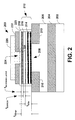
- the transistor 200 comprises a semiconductor substrate, for example, a p-type lightly doped silicon substrate.
- An isolation region 204 for example, a buried oxide layer is formed in the substrate 202 , however, the isolation region 204 is optional for the present invention.
- a p-type collector region 206 is formed over the isolation region 204 .
- the collector 206 is initially part of the substrate 202 and is subsequently defined by the formation of the buried oxide layer 204 , however, the collector region 206 alternatively may be formed via an epitaxial growth process, as may be desired.
- a collector region interface 208 is defined by the formation of laterally spaced isolation regions 210 via, for example, a shallow trench isolation process.
- a SiGe strain layer (which may alternatively be referred to as the emitter/base epi region) 212 is then formed over the collector region interface 208 .
- the SiGe strain layer 212 comprises a graded profile SiGe layer 214 , an intrinsic Si buffer layer 216 formed thereover, and a diffusion blocking layer 218 formed over the buffer layer 216 .
- the buffer layer 216 may be substantially eliminated with the diffusion blocking layer 218 overlying the SiGe graded profile base layer 214 , more directly.
- the diffusion blocking layer 218 advantageously mitigates or altogether eliminates a diffusion of p-type dopant from the emitter to the SiGe base layer 214 , thereby allowing for an advantageous reduction in emitter/base epi layer thickness.
- a pad oxide adhesion layer 220 is formed over the diffusion blocking layer 218 , and a nitride layer 222 is further formed over the oxide 220 .
- the isolation layers 220 and 222 may be formed as illustrated, it should be understood that other isolation materials and layer combinations may be utilized in order to define an emitter contact region and any such alternatives are contemplated as falling within the scope of the present invention.
- An emitter contact region 224 is then defined in the isolation layers 220 and 222 and an emitter region, for example, a doped polysilicon layer 226 is formed thereover, thereby making electrical contact down to the SiGe strain layer 212 via the diffusion blocking layer 218 .
- the PNP heterojunction bipolar transistor 200 of FIG. 2 advantageously overcomes several of the disadvantages associated with the prior art transistor 100 of FIG. 1 .
- the diffusion blocking layer 218 is operable to retard the diffusion of p-type dopants such as boron from the emitter region 226 to ensure dopants do not reach the SiGe base layer 214 and therefore the thickness of the layer 216 (t BUFFER ) is substantially reduced or eliminated altogether.
- the intrinsic Si buffer layer 216 may be reduced from about 400 Angstroms in prior art FIG. 1 to about 50 Angstroms (e.g., about 0-100 Angstroms). Consequently, the SiGe strain layer thickness t EB-epi is reduced substantially.
- the buffer layer 216 may be removed completely, thereby further reducing the SiGe strain layer thickness (t EB-epi ).
- the blocking layer 216 thickness may be a function of the thermal budget of the process, wherein if subsequent processing steps require substantial thermal processing, the blocking layer thickness may need to be increased, and wherein if subsequent steps require lesser amounts (or lesser temperatures) for thermal processing, the blocking layer thickness may be further reduced or eliminated completely.
- the diffusion blocking layer 218 may comprise a silicon-carbon alloy (SiC).
- SiC silicon-carbon alloy
- the SiC may have a thickness of about 50 Angstroms and have a composition of Si (1-X) C X , wherein X varies between about 0.0001 and about 0.01, and more particularly between about 0.001 to about 0.002.
- a diffusion blocking layer which operates to retard or eliminate a diffusion of p-type dopants such as boron therethrough
- a SiGe alloy or other suitable type material may be employed to retard diffusion.
- the diffusion of dopants into the diffusion blocking layer 218 causes the layer 218 to be a part of the emitter (often called the emitter-epi). This phenomena advantageously moves the depletion region away from the emitter polysilicon interface which further improves transistor performance.
- t EB-epi a reduction in the SiGe strain layer thickness results in less lattice stress and thus permits a higher germanium concentration in the graded SiGe base layer 214 over the conventional structure 100 of prior art FIG. 1 .
- improved transistor speed is attained without sacrificing the quality of the SiGe strain layer 212 ; that is, the Ge concentration is increased without a substantial increase in defect density therein.
- a generally trapezoidal shaped SiGe graded profile base layer 214 may be employed, wherein the Ge concentration increases at a high rate near the collector region interface 208 and gradually decreases in concentration as one traverses the SiGe strain layer 212 vertically toward the emitter-poly region 226 .
- the transistor structure 200 of FIG. 2 also exhibits reduced emitter resistance over the prior art device 100 of FIG. 1 .
- the emitter-poly 226 contacts substantially directly the diffusion blocking layer 218 , for example, a SiC alloy. Due to the composition of the blocking layer 218 , its surface does not oxidize as readily as the exposed intrinsic Si buffer layer of the prior art, and thus little substantial interfacial oxide forms and resides at the emitter/blocking layer interface 228 . What oxide is present is more easily removed in the epi reactor chamber prior to emitter poly deposition. Thus the resistance between the emitter 228 and the SiGe strain layer 212 is reduced substantially.
- FIG. 3 a flow chart diagram is provided which illustrates a method 300 of forming a PNP type heterojunction bipolar transistor having a reduced emitter/base epi thickness according to the present invention.
- the method 300 of FIG. 3 will be described in conjunction with other figures in order to facilitate a clear understanding of the present invention, however, such accompanying figures are not meant to limit the scope of the invention and should not be interpreted as such.
- the methodology of FIG. 3 is shown and described in a serial manner, it is to be understood and appreciated that the present invention is not limited by the illustrated order, as some aspects could, in accordance with the present invention, occur in different orders and/or concurrently with other aspects from that shown and described herein.
- not all illustrated features may be required to implement a methodology in accordance with an aspect of the present invention.
- the method 300 begins at step 302 with the formation and/or definition of a collector region (e.g., collector region 206 of FIG. 2 ).
- a semiconductor substrate 310 e.g., a lightly doped p-type Si substrate
- the formation of the buried oxide layer 312 separates the substrate 310 into two sections, a lower region 314 which acts as the device substrate, and an upper region 316 which defines a lightly doped p-type collector region.
- the collector region may be subsequently doped to customize the collector dopant concentration if desired.
- Step 302 continues further by defining the collector region to form a collector interface.
- a shallow trench isolation process may be employed by anisotropically etching shallow trenches 318 into the collector region 316 using, for example, a dry etch.
- a chemical vapor deposition step is performed, by which an oxide layer is formed over the substrate 310 and then etched by using either an etch or a chemical-mechanical polishing (CMP) step to substantially planarize the substrate surface, wherein the surface is defined by two laterally spaced isolation regions 320 and a collector interface region 322 .
- CMP chemical-mechanical polishing
- the method 300 of FIG. 3 continues at steps 330 and 332 by forming a graded profile base region (e.g., a portion of the SiGe strain layer 212 of FIG. 2) over the defined collector region and a diffusion blocking layer over the graded profile base region.
- a graded profile base region e.g., a portion of the SiGe strain layer 212 of FIG. 2
- the graded profile base region and diffusion blocking layer may be formed via numerous techniques and all such techniques are contemplated as falling within the scope of the present invention, however, one exemplary method will be discussed and illustrated in conjunction with FIGS. 7-10.
- the formation of the graded profile base region may be formed in accordance with one exemplary aspect of the present invention using a vapor phase epitaxy deposition (VPE) process, however, other processes may be employed (e.g., limited reaction processing (LRP), molecular beam epitaxy (MBE), laser melting, and others) and are contemplated as falling within the scope of the present invention.
- VPE vapor phase epitaxy deposition
- LRP limited reaction processing
- MBE molecular beam epitaxy
- laser melting laser melting
- the VPE process at step 334 is initiated by setting the epi-reactor chamber to a desired chamber pressure (e.g., about 10-20 Torr, or alternatively atmospheric pressure) and activating both silicon and germanium gas sources.
- a desired chamber pressure e.g., about 10-20 Torr, or alternatively atmospheric pressure
- the base layer (e.g., graded profile base layer 214 of FIG. 2) is generated with a graded profile at step 336 by dynamically controlling the Si and Ge source gases so as to introduce a varying Si/Ge ratio as the epitaxial layer grows.
- step 336 may have a substantially low Si/Ge ratio (indicating a larger Ge concentration) initially and then gradually increase the Si/Ge ratio over time to generate a generally trapezoidal graded profile, wherein a concentration of Ge in the SiGe alloy decreases as the layer is formed.
- the layer formation process results in a SiGe graded profile base layer 338 , as illustrated in FIG. 8 having a thickness t SiGe (e.g., about 1000 Angstroms or less).
- the Ge source is deactivated at step 340 .
- the diffusion blocking layer (e.g., layer 218 of FIG. 2) is then formed by initiating a blocking material source gas associated with the VPE process at step 342 .
- the blocking material source gases are methyl silane and dichlorosilane and/or silane, such that the resulting layer is a SiC alloy.
- the Si/C source gas ratio is such that the resulting SiC alloy is Si (1-X) C X , wherein X varies between about 0.0001 and about 0.01, and more particularly between about 0.001 and about 0.002.
- step 342 is controlled so as to generate a diffusion blocking layer 347 of a predetermined thickness (t BLOCKING LAYER ) (e.g., about 50 Angstroms), as illustrated in FIG. 10 .
- t BLOCKING LAYER a predetermined thickness
- the thickness of the blocking layer 347 is chosen to enhance the ability to retard diffusion therethrough, yet thin enough to maintain favorable transistor operating characteristics. Therefore the blocking layer thickness may vary based on custom requirements, process thermal budget and the type of material used therein.
- the blocking layer 347 does not block diffusion in the literal sense. Rather the layer 347 reduces the diffusion therethrough to the underlying layer. Therefore the layer 347 controls the diffusion of p-type dopants from the emitter poly down to the underlying epi. By slowing the diffusion through the blocking layer, the p-type dopants slow down, causing the dopants therein to build up and form a substantially abrupt junction. Therefore the blocking layer 347 becomes part of the emitter (often called the emitter-epi).
- the introduction of the blocking material source gas may be introduced after a predetermined delay, during which time an intrinsic Si buffer layer 344 may be formed over the SiGe graded profile base layer 338 as illustrated in FIG. 9 .
- a buffer layer 344 may be optional based on the efficacy of the subsequently formed diffusion blocking layer 347 . That is, if the diffusion blocking layer 347 is operable to completely block all diffusion of p-type dopants such as boron therethrough, then no buffer layer 344 is necessary. However, if the blocking layer 347 instead is only operable to mitigate the diffusion, a nominal intrinsic Si buffer layer 344 may be employed and may be included by delaying a timing at which the blocking material source gas is introduced at step 342 .
- the blocking material source gas is discontinued and the Si source gas feed is maintained for another predetermined time to generate an intrinsic Si layer 348 at step 349 over the diffusion blocking layer 344 , as illustrated in FIG. 10 having a predetermined thickness (e.g., about 45 Angstroms).
- the Si layer 348 will subsequently be consumed, but will help facilitate a low resistance emitter/base interface.
- an emitter/base epi region layer having an alloy concentration which varies therethrough is achieved.
- the concentration may be similar to that illustrated in FIG. 11 .
- a concentration profile 350 is illustrated, wherein a germanium concentration 352 in the SiGe base layer (e.g., layer 214 of FIG. 2 or layer 338 of FIG. 10) varies as one traverses from the collector toward the emitter. Note that at one side 354 near the collector, the Ge concentration rises rapidly to a maximum 356 at a thickness of about 100 Angstroms and then gradually decreases over the next 600 Angstroms to form a generally trapezoidal shaped graded profile.
- This buffer layer in accordance with one exemplary aspect of the present invention is about 200 Angstroms thick, but this thickness may decrease or be eliminated altogether based on an effectiveness of the diffusion blocking layer.
- the concentration profile of FIG. 11 also has another impurity concentration region 360 which corresponds to the diffusion blocking layer (e.g., layer 218 of FIG. 2 or layer 347 of FIG. 10 ).
- the impurity may be carbon or other materials which operate to retard the diffusion of p-type dopants therethrough.
- the thickness of the diffusion blocking layer may be about 50 Angstroms.
- the concentration profile of FIG. 11 illustrates an intrinsic Si region 362 at a top portion of the emitter/base layer, which operates as an interface to the emitter region. As will be discussed in greater detail infra, this region 362 will subsequently be consumed in the formation of the emitter contact region to minimize the emitter resistance associated with the transistor.
- subsequent processing will cause diffusion from the emitter into the diffusion blocking layer such that the blocking layer becomes part of the emitter (often called the emitter-epi region) such that the depletion region advantageously forms therein during transistor operation.
- step 360 by forming isolation over the diffusion blocking layer 347 (and Si layer 348 of FIG. 10) and defining an emitter contact region therein at step 366 .
- the steps 360 and 366 will be described in conjunction with FIGS. 12-17.
- step 360 may comprise forming a pad oxide adhesion layer 362 as an etch stop layer (step 370 in FIG. 12) via, for example, oxide growth in a furnace and depositing a silicon nitride layer 364 thereover at step 372 , as illustrated in FIG. 13 .
- An emitter contact region is then defined at step 374 by selectively etching through the nitride layer 364 , using the underlying oxide layer 362 as an etch stop as illustrated in FIG. 14 . That is, the etch is selective with respect to the oxide such that an overetch may be utilized to ensure complete removal of the nitride in region 368 without substantial concern of etching through the oxide layer 364 .
- Step 366 continues at step 376 by performing a deglaze step to remove the exposed silicon oxide which still remains after the nitride removal.
- the deglaze may comprise a wet HF etchant solution which removes the oxide in the region 368 to expose the underlying intrinsic silicon layer 348 , as illustrated in FIG. 15, however, other processes and/or etchants may be employed and are contemplated as falling within the scope of the present invention.
- the exposed silicon layer 348 is then oxidized at step 378 via, for example, thermal processing to generate a silicon dioxide region 380 , as illustrated in FIG. 16 in region 368 .
- the silicon dioxide region 380 is then removed by another deglaze step 382 to thereby expose the underlying diffusion blocking layer 347 (e.g., SiC), as illustrated in FIG. 17 . Because the diffusion blocking layer 347 is substantially less susceptible to oxidation, a substantially lower resistance emitter/base interface may be formed, thereby further improving the transistor performance over the prior art.
- the diffusion blocking layer 347 e.g., SiC
- the method 300 continues at step 390 by forming an emitter polysilicon region 392 over the defined emitter contact region, as illustrated in FIG. 18 .
- a polysilicon layer may be deposited via CVD and doped with a p-type dopant such as boron (either in-situ or in a subsequent implantation step).
- the implanted dopant is then diffused through the polysilicon into the base/emitter epi layer via a thermal processing step.
- the p-type dopant does not diffuse substantially through the diffusion blocking layer 347 , thereby allowing an underlying intrinsic Si buffer layer 344 to be substantially minimized or eliminated altogether.
- the method 300 of the present invention provides for the fabrication of a PNP heterojunction bipolar transistor structure, which enables a reduction in the emitter/base epi thickness and an increase in the peak Ge concentration in the graded profile base layer.
- the position of the emitter p-n junction is well controlled, providing greater process margin. Higher diffusion temperatures may be used to achieve the desired dopant profile at a higher boron dopant activation.
- the emitter side of the depletion region is more abrupt therefore yielding a device which has significantly higher gain.
- the method 300 provides for a reduced emitter resistance over the prior art by eliminating an interfacial oxide at the emitter/base interface.
- the above aspects of the present invention are not limited to heterojunction bipolar transistor structures, but rather they apply to any form of PNP transistor structure where p-type dopants such as boron diffuse from the emitter poly into the emitter/base epi. Therefore a traditional PNP transistor structure may employ a diffusion blocking layer as highlighted above, and such a structure is contemplated as falling within the scope of the present invention.
- the method of the present invention may be employed within a complimentary bipolar transistor process without impacting adversely the formation of NPN type transistors. Incorporation of the above aspects of the invention into such a complimentary bipolar process is contemplated as falling within the scope of the present invention.
Abstract
The present invention relates to a method of forming a bipolar transistor or a heterojunction bipolar transistor. The method comprises forming a collector region associated with a semiconductor substrate, and forming a base region base region over at least a portion of the collector region. The method further comprises forming a diffusion blocking layer over the base region, and forming an emitter polysilicon region over the diffusion blocking layer. The diffusion blocking layer reduces an amount of diffusion from the emitter polysilicon region into the base region, thereby allowing improved process control and emitter/base doping profile, leading to improved transistor performance. In addition, the present invention relates to a heterojunction bipolar transistor, and comprises a collector region, and a graded profile SiGe base layer overlying the collector region. The transistor further comprises a diffusion blocking layer overlying the graded profile SiGe base layer, and an emitter layer overlying the diffusion blocking layer. The diffusion blocking layer is operable to retard a diffusion of dopants therethrough from the emitter layer to the graded profile SiGe base layer, thereby allowing for a reduction in the thickness of the layer comprising a graded profile SiGe layer and a buffer layer. The thickness reduction allows increased Ge concentration in the base layer and the emitter/base doping profile is improved, each leading to improved transistor performance.
Description
The present invention relates in general to the field of integrated circuits, and more particularly to bipolar and heterojunction bipolar transistor structures and a method of fabricating such structures.
Bipolar transistors are important components in, for example, logic circuits, communications systems, and microwave devices. A bipolar transistor is essentially a three terminal device having three regions, an emitter, base and collector region, wherein the emitter and collector regions are of one conductivity type and the base is of another.
Since the advent of bipolar transistors, many attempts have been made to improve the performance of the transistor. Some of these attempts have focused on increasing the current gain by improving the injection efficiency of the minority carriers from the emitter to the base. In order to accomplish this, wide bandgap transistors have been fabricated wherein the bandgap of the emitter is wider than the bandgap of the base. A wide bandgap transistor has been constructed in a variety of fashions, and one such transistor structure is referred to as a heterojunction bipolar transistor.
For example, in one type of heterojunction transistor, a transistor is formed with a silicon collector region, a base region composed of a silicon-germanium (SiGe) alloy, and a silicon emitter region. The mixed crystal semiconductor base layer may have a uniform distribution of germanium in silicon or may contain a graded distribution of germanium in the silicon. The graded SiGe distribution is provided in order to increase the bandgap of the transistor. With the above described structure of a wide bandgap transistor and the fact that germanium has a large electron mobility, performance of the transistor is enhanced.
A brief explanation of how the SiGe base region enhances transistor performance is provided briefly below. Graded junctions are used in solid state transistors to enhance device performance. The application of a graded junction in the base region of a bipolar transistor, for example, results in the formation of a nonuniform energy gap. A graded bandgap can be employed to reduce base transit time and thus increase the device speed. More particularly, the bandgap of silicon can be varied by the introduction of dopants, the formation of alloys (e.g., SiGe), and/or the introduction of strain into the crystal lattice. Combinations of all three of these phenomena have been used to produce very high speed graded SiGe-base heterojunction bipolar transistors. In addition, such graded profile heterojunction transistors may exhibit additional advantages over conventional silicon devices for high speed digital and microwave devices, for example, by providing higher emitter injection efficiency, lower base resistance, lower base transit times, and superior low temperature speed and gain.
Many attempts in further improving heterojunction bipolar transistor performance have focused on, for example, decreasing the width of the base region of a transistor and decreasing the base transit time for a constant base width. Nevertheless, accomplishing such a base thickness reduction has proved difficult for a variety of technical reasons. For example, anneal processes involved in polysilicon type emitter PNP bipolar devices may result in the P-type emitter dopant (e.g., boron) diffusing into the base region. To mitigate the negative impact of such diffusion, an intrinsic silicon buffer layer is typically added to the graded profile base region to prevent such diffusion from negatively impacting the SiGe alloy. Such a buffer layer, however, causes the effective emitter/base epitaxy thickness to increase. Therefore, in conventional heterojunction structures and methods, there is a limitation as to how thin the emitter/base epitaxy can be fabricated when the emitter is formed and contacted by polysilicon.
There is a need in the art for improved structures and methods relating to heterojunction bipolar transistors.
The present invention relates generally to a bipolar transistor structure and a method of making such a structure, which reduces the base transit time and provides for a more abrupt emitter-base junction, and hence higher transition frequency and gain.
The present invention is directed to a heterojunction bipolar transistor structure having a diffusion blocking layer (e.g., a SiC alloy) associated with the emitter/base region of the transistor. The diffusion blocking layer is operable to retard a diffusion of dopants therethrough from the emitter region down to a SiGe graded profile base layer. The reduction in diffusion allows a buffer layer associated with the emitter/base epi region to be reduced substantially, thereby reducing the emitter/base epi thickness. The emitter/base epi thickness reduction advantageously improves transistor performance and reduces the lattice strain in the base, thereby permitting a peak germanium concentration in the SiGe graded profile base layer to be increased, which advantageously increases the transistor speed and/or gain. In addition, the method employs an intrinsic silicon layer over the diffusion blocking layer in the emitter/base epi region to form an oxide which is then removed with a deglaze step. The oxidation and deglaze steps expose the underlying diffusion blocking layer which is not prone to oxidation prior to formation of the emitter, thereby reducing or eliminating an interfacial oxide at the emitter/emitter poly interface and reducing the emitter resistance of the transistor.
To the accomplishment of the foregoing and related ends, the invention comprises the features hereinafter fully described and particularly pointed out in the claims. The following description and the annexed drawings set forth in detail certain illustrative aspects and implementations of the invention. These are indicative, however, of but a few of the various ways in which the principles of the invention may be employed. Other objects, advantages and novel features of the invention will become apparent from the following detailed description of the invention when considered in conjunction with the drawings.
FIG. 1 is a fragmentary cross section diagram illustrating a prior art heterojunction bipolar transistor structure;
FIG. 2 is a fragmentary cross section diagram illustrating a heterojunction bipolar transistor structure according to one exemplary aspect of the present invention;
FIG. 3 is a flow chart diagram illustrating a method of fabricating a heterojunction, bipolar transistor structure such as that illustrated in FIG. 2 according to one exemplary aspect of the present invention;
FIG. 4 is a fragmentary cross section diagram illustrating a step of forming a collector region according to the present invention;
FIG. 5 is a fragmentary cross section diagram illustrating a step of defining collector region interface according to the present invention;
FIG. 6 is a fragmentary cross section diagram illustrating a step of further defining the collection region interface using a shallow trench isolation process according to the present invention;
FIG. 7 is a flow chart diagram illustrating a method of forming a graded profile base region and a diffusion blocking layer such as that illustrated in FIG. 2 according to one exemplary aspect of the present invention;
FIG. 8 is a fragmentary cross section diagram illustrating a step of forming a graded profile base layer according to the present invention;
FIG. 9 is a fragmentary cross section diagram illustrating a step of forming a diffusion blocking layer and an intrinsic silicon buffer layer, if needed, according to the present invention;
FIG. 10 is a fragmentary cross section diagram illustrating a step of forming an intrinsic silicon layer over the diffusion blocking layer according to the present invention;
FIG. 11 is a graph illustrating a concentration profile associated with the base region of he heterojunction bipolar transistor according to one exemplary aspect of the present invention;
FIG. 12 is a flow chart diagram illustrating a method of forming an isolation region and defining an emitter contact region therein according to the present invention;
FIG. 13 is a fragmentary cross section diagram illustrating the isolation region overlying the emitter/base epi region of the transistor according to the present invention;
FIG. 14 is a fragmentary cross section diagram illustrating a selective etching of a nitride region using an underlying oxide layer as an etch stop according to the present invention;
FIG. 15 is a fragmentary cross section diagram illustrating a deglaze step by which a portion of an oxide region is removed to expose an underlying intrinsic silicon layer according to the present invention;
FIG. 16 is a fragmentary cross section diagram illustrating an oxidation of the exposed intrinsic silicon layer to form an oxide according to the present invention;
FIG. 17 is a fragmentary cross section diagram illustrating another deglaze step by which the oxide region is removed to expose an underlying diffusion blocking layer which is substantially resistant to oxidation according to the present invention; and
FIG. 18 is a fragmentary cross section diagram illustrating a doped polysilicon emitter region formed over the transistor, wherein the dopant from the emitter does not substantially diffuse through the diffusion blocking layer, thereby allowing the effective emitter/base epitaxy thickness to be reduced according to the present invention.
The present invention will now be described with respect to the accompanying drawings in which like numbered elements represent like parts.
The present invention is directed to a bipolar or a heterojunction bipolar transistor structure and a method of manufacturing such a structure which exhibits improved transistor performance due to a reduction in the transistor emitter/base epitaxy thickness and a more abrupt emitter/base junction. More particularly, the transistor comprises a diffusion blocking layer associated with the emitter/base epitaxy region which impedes the diffusion of dopants such as boron from the emitter polysilicon down to a graded profile SiGe base layer. The reduction in dopant diffusion allows for a reduction or elimination of a silicon buffer layer associated with the emitter/base epitaxy region, which reduces the emitter/base epi thickness. In addition, the reduction in emitter/base epi thickness reduces strain in the SiGe graded profile base layer, thereby allowing a peak germanium concentration therein to be increased, which provides for an increase in transistor speed and/or gain. The position of the emitter p-n junction is well controlled, providing greater process margin. Higher diffusion temperatures may be used to achieve the desired dopant profile at a higher boron dopant activation. Also, the emitter side of the depletion region is more abrupt therefore yielding a device which has significantly higher gain.
In order to properly understand the various advantageous inventive aspects of the present invention, a brief description of a conventional PNP type heterojunction bipolar transistor structure will be described, along with an exemplary processing methodology discussion where appropriate. A conventional heterojunction bipolar transistor structure is illustrated in prior art FIG. 1, and is designated at reference numeral 100. The transistor 100 is formed on a semiconductor substrate, for example, a lightly doped p-type silicon substrate 102 with an isolation region formed therein, for example, a buried oxide layer 104. A p-type collector region 106 is formed over the buried oxide layer 104, and a collector interface 108 is defined by the formation of laterally spaced isolation regions 110.
An n-type SiGe strain layer (sometimes referred to as an emitter/base layer) 112 is then formed over the collector interface 108. The SiGe strain layer 112 includes, for example, a graded profile SiGe layer 114 and an intrinsic silicon buffer layer 116 thereon. A thin pad oxide adhesion layer 118 overlies the SiGe strain layer 112 and another isolation region, for example, a nitride layer 120 overlies the oxide layer 118. A p-type polysilicon emitter region 122 then makes contact to the SiGe strain layer 112 through a contact region 124 in the isolation layers 116 and 118, respectively.
The conventional heterojunction bipolar transistor structure 100 of prior art FIG. 1 has several drawbacks. Initially, the SiGe strain layer 112 is undesirably thick due to the nature of the structure, and reducing such thickness is prohibitive. The SiGe strain layer 112 has a thickness TEB-epi, which is defined by a SiGe layer 114 of thickness tSiGe and the intrinsic Si buffer layer 116 of thickness tBUFFER. The buffer layer 116 serves to accommodate p-type dopant (e.g., boron) which diffuses from the emitter polysilicon 122 into the SiGe strain layer 112 to form the epitaxial emitter 126. Because boron readily diffuses from the polysilicon emitter 122 into the SiGe strain layer 112 during the thermal anneal of the emitter 122, the intrinsic Si buffer layer 116 receives the diffused dopant and prevents such dopant from reaching the SiGe layer 114, wherein such dopant would negatively impact transistor performance. Typically, to prevent boron diffusion down to the SiGe layer 114, the intrinsic Si buffer layer 116 exhibits a thickness (tBUFFER) of about 400 Angstroms (e.g., 300-500 Angstroms) or so. Therefore for a SiGe layer 114 having a given thickness (e.g., about 1,300 Angstroms), a buffer layer of about 400 Angstroms or so is required to maintain performance integrity. Since the SiGe strain layer thickness (tEB-epi) is a function of both the buffer layer 116 and the SiGe layer 114 (tEB-epi=tBUFFER+tSiGe), the required buffer layer thickness acts as a limiting factor on decreasing the emitter/base epi thickness.
In addition, the thickness of the intrinsic Si buffer layer 116 limits an amount of lattice mismatch between the bulk Si in the collector and the SiGe layer 114 due to stress issues. Therefore the buffer layer 116 reduces the peak Ge concentration which can be integrated into the SiGe layer 116. As is well known, when forming a layer on another layer which do not have matching crystal lattices (e.g., a Si collector and a SiGe base) a lattice strain will occur. In such a context, there is a critical thickness at which the lattice strain will cause a nucleation of defects in the growing epitaxial layer. These defects will quickly multiply so that the resulting layer will exhibit undesirably high defect levels. If, however, the thickness of the epitaxial layer is less than the critical thickness, there can be a very low defect density in the epitaxial layer.
The critical thickness of the epitaxial layer depends on the degree of lattice mismatch. Therefore for relatively pure Ge grown on Si, which exhibit about a 4% lattice mismatch, only about 5-6 atomic layers of Ge can be formed on the Si. However, in a SiGe alloy for low concentrations of Ge, the critical thickness of the film may be increased since the degree of lattice strain is less. Therefore it can be seen that an inverse relationship exists between the Ge concentration in a SiGe alloy and a critical thickness at which defect density is unreasonably high. Applying this relationship to the structure 100 of prior art FIG. 1, it can be seen that as the SiGe strain layer (emitter/base epi layer) thickness (tEB-epi) is increased due to the necessary buffer layer 116, the Ge concentration in the SiGe layer 114 must be undesirably decreased to avoid an undesirably large defect density therein due to lattice strain. Such a decrease in Ge concentration negatively impacts transistor speed.
In addition to the disadvantages highlighted above, the heterojunction bipolar transistor 100 of prior art FIG. 1 also exhibits an undesirably large emitter resistance due to an oxidation region 126 at the emitter poly/emitter epi layer interface. When forming the transistor 100, the pad oxide adhesion layer 118 is formed over the SiGe strain layer 112 and a nitride layer 120 is then formed on the oxide 118. When defining the emitter contact, the oxide 118 serves as an etch stop, wherein the dry etch is substantially selective with respect to the oxide, thereby allowing an overetch of the nitride 120 to occur without a substantial risk of etching into the buffer layer 116. Although the remaining oxide 118 is subsequently removed, the underlying layer 116 is intrinsic silicon which naturally oxidizes when exposed to various environmental conditions, and forms a thin native oxide (e.g., about 5-10 Angstroms) thereover. This interfacial oxide 126 undesirably results in an increase in the emitter resistance.
Turning now to FIG. 2, a PNP type heterojunction bipolar transistor 200 according to the present invention is disclosed. The transistor 200 comprises a semiconductor substrate, for example, a p-type lightly doped silicon substrate. An isolation region 204, for example, a buried oxide layer is formed in the substrate 202, however, the isolation region 204 is optional for the present invention. A p-type collector region 206 is formed over the isolation region 204. According to one exemplary aspect of the present invention, the collector 206 is initially part of the substrate 202 and is subsequently defined by the formation of the buried oxide layer 204, however, the collector region 206 alternatively may be formed via an epitaxial growth process, as may be desired.
Still referring to FIG. 2, a collector region interface 208 is defined by the formation of laterally spaced isolation regions 210 via, for example, a shallow trench isolation process. A SiGe strain layer (which may alternatively be referred to as the emitter/base epi region) 212 is then formed over the collector region interface 208. According to one exemplary aspect of the present invention, the SiGe strain layer 212 comprises a graded profile SiGe layer 214, an intrinsic Si buffer layer 216 formed thereover, and a diffusion blocking layer 218 formed over the buffer layer 216. Alternatively, the buffer layer 216 may be substantially eliminated with the diffusion blocking layer 218 overlying the SiGe graded profile base layer 214, more directly. As will be discussed in greater detail infra, the diffusion blocking layer 218 advantageously mitigates or altogether eliminates a diffusion of p-type dopant from the emitter to the SiGe base layer 214, thereby allowing for an advantageous reduction in emitter/base epi layer thickness.
A pad oxide adhesion layer 220 is formed over the diffusion blocking layer 218, and a nitride layer 222 is further formed over the oxide 220. Although the isolation layers 220 and 222 may be formed as illustrated, it should be understood that other isolation materials and layer combinations may be utilized in order to define an emitter contact region and any such alternatives are contemplated as falling within the scope of the present invention. An emitter contact region 224 is then defined in the isolation layers 220 and 222 and an emitter region, for example, a doped polysilicon layer 226 is formed thereover, thereby making electrical contact down to the SiGe strain layer 212 via the diffusion blocking layer 218.
The PNP heterojunction bipolar transistor 200 of FIG. 2 advantageously overcomes several of the disadvantages associated with the prior art transistor 100 of FIG. 1. For example, the diffusion blocking layer 218 is operable to retard the diffusion of p-type dopants such as boron from the emitter region 226 to ensure dopants do not reach the SiGe base layer 214 and therefore the thickness of the layer 216 (tBUFFER) is substantially reduced or eliminated altogether. For example, the intrinsic Si buffer layer 216 may be reduced from about 400 Angstroms in prior art FIG. 1 to about 50 Angstroms (e.g., about 0-100 Angstroms). Consequently, the SiGe strain layer thickness tEB-epi is reduced substantially. Clearly, if the diffusion blocking layer 218 is sufficiently effective to completely prohibit diffusion therethrough, the buffer layer 216 may be removed completely, thereby further reducing the SiGe strain layer thickness (tEB-epi).
As may be appreciated, the blocking layer 216 thickness may be a function of the thermal budget of the process, wherein if subsequent processing steps require substantial thermal processing, the blocking layer thickness may need to be increased, and wherein if subsequent steps require lesser amounts (or lesser temperatures) for thermal processing, the blocking layer thickness may be further reduced or eliminated completely.
According to one exemplary aspect of the present invention, the diffusion blocking layer 218 may comprise a silicon-carbon alloy (SiC). For example, the SiC may have a thickness of about 50 Angstroms and have a composition of Si(1-X)CX, wherein X varies between about 0.0001 and about 0.01, and more particularly between about 0.001 to about 0.002. Although the above composition type and relative amount is one example of a diffusion blocking layer which operates to retard or eliminate a diffusion of p-type dopants such as boron therethrough, it should be understood that other materials or alloys may be employed and are contemplated as falling within the scope of the present invention. For example, a SiGe alloy or other suitable type material may be employed to retard diffusion.
Note the diffusion of dopants into the diffusion blocking layer 218 (e.g., the SiC layer) causes the layer 218 to be a part of the emitter (often called the emitter-epi). This phenomena advantageously moves the depletion region away from the emitter polysilicon interface which further improves transistor performance.
As highlighted above, a reduction in the SiGe strain layer thickness (tEB-epi) results in less lattice stress and thus permits a higher germanium concentration in the graded SiGe base layer 214 over the conventional structure 100 of prior art FIG. 1. By employing a higher Ge concentration in the SiGe base layer 214, improved transistor speed is attained without sacrificing the quality of the SiGe strain layer 212; that is, the Ge concentration is increased without a substantial increase in defect density therein. According to one exemplary aspect of the present invention, a generally trapezoidal shaped SiGe graded profile base layer 214 may be employed, wherein the Ge concentration increases at a high rate near the collector region interface 208 and gradually decreases in concentration as one traverses the SiGe strain layer 212 vertically toward the emitter-poly region 226.
The transistor structure 200 of FIG. 2 also exhibits reduced emitter resistance over the prior art device 100 of FIG. 1. In the transistor 200, the emitter-poly 226 contacts substantially directly the diffusion blocking layer 218, for example, a SiC alloy. Due to the composition of the blocking layer 218, its surface does not oxidize as readily as the exposed intrinsic Si buffer layer of the prior art, and thus little substantial interfacial oxide forms and resides at the emitter/blocking layer interface 228. What oxide is present is more easily removed in the epi reactor chamber prior to emitter poly deposition. Thus the resistance between the emitter 228 and the SiGe strain layer 212 is reduced substantially.
Turning now to FIG. 3, a flow chart diagram is provided which illustrates a method 300 of forming a PNP type heterojunction bipolar transistor having a reduced emitter/base epi thickness according to the present invention. The method 300 of FIG. 3 will be described in conjunction with other figures in order to facilitate a clear understanding of the present invention, however, such accompanying figures are not meant to limit the scope of the invention and should not be interpreted as such. In addition, while for purposes of simplicity of explanation the methodology of FIG. 3 is shown and described in a serial manner, it is to be understood and appreciated that the present invention is not limited by the illustrated order, as some aspects could, in accordance with the present invention, occur in different orders and/or concurrently with other aspects from that shown and described herein. Moreover, not all illustrated features may be required to implement a methodology in accordance with an aspect of the present invention.
The method 300 begins at step 302 with the formation and/or definition of a collector region (e.g., collector region 206 of FIG. 2). For example, as illustrated in FIG. 4, a semiconductor substrate 310 (e.g., a lightly doped p-type Si substrate) has a buried oxide layer 312 formed therein using one of several known, conventional techniques. The formation of the buried oxide layer 312 separates the substrate 310 into two sections, a lower region 314 which acts as the device substrate, and an upper region 316 which defines a lightly doped p-type collector region. The collector region may be subsequently doped to customize the collector dopant concentration if desired.
Step 302 continues further by defining the collector region to form a collector interface. For example, as illustrated in FIGS. 5 and 6, a shallow trench isolation process may be employed by anisotropically etching shallow trenches 318 into the collector region 316 using, for example, a dry etch. Subsequently, a chemical vapor deposition step is performed, by which an oxide layer is formed over the substrate 310 and then etched by using either an etch or a chemical-mechanical polishing (CMP) step to substantially planarize the substrate surface, wherein the surface is defined by two laterally spaced isolation regions 320 and a collector interface region 322.
The method 300 of FIG. 3 continues at steps 330 and 332 by forming a graded profile base region (e.g., a portion of the SiGe strain layer 212 of FIG. 2) over the defined collector region and a diffusion blocking layer over the graded profile base region. The graded profile base region and diffusion blocking layer may be formed via numerous techniques and all such techniques are contemplated as falling within the scope of the present invention, however, one exemplary method will be discussed and illustrated in conjunction with FIGS. 7-10.
The formation of the graded profile base region may be formed in accordance with one exemplary aspect of the present invention using a vapor phase epitaxy deposition (VPE) process, however, other processes may be employed (e.g., limited reaction processing (LRP), molecular beam epitaxy (MBE), laser melting, and others) and are contemplated as falling within the scope of the present invention. The VPE process at step 334 is initiated by setting the epi-reactor chamber to a desired chamber pressure (e.g., about 10-20 Torr, or alternatively atmospheric pressure) and activating both silicon and germanium gas sources.
The base layer (e.g., graded profile base layer 214 of FIG. 2) is generated with a graded profile at step 336 by dynamically controlling the Si and Ge source gases so as to introduce a varying Si/Ge ratio as the epitaxial layer grows. For example, step 336 may have a substantially low Si/Ge ratio (indicating a larger Ge concentration) initially and then gradually increase the Si/Ge ratio over time to generate a generally trapezoidal graded profile, wherein a concentration of Ge in the SiGe alloy decreases as the layer is formed. The layer formation process results in a SiGe graded profile base layer 338, as illustrated in FIG. 8 having a thickness tSiGe (e.g., about 1000 Angstroms or less). After a predetermined period of time has elapsed which corresponds to a desired thickness of the SiGe layer, the Ge source is deactivated at step 340.
The diffusion blocking layer (e.g., layer 218 of FIG. 2) is then formed by initiating a blocking material source gas associated with the VPE process at step 342. According to one exemplary aspect of the present invention, the blocking material source gases are methyl silane and dichlorosilane and/or silane, such that the resulting layer is a SiC alloy. Further, in accordance with one exemplary aspect of the invention, the Si/C source gas ratio is such that the resulting SiC alloy is Si(1-X)CX, wherein X varies between about 0.0001 and about 0.01, and more particularly between about 0.001 and about 0.002. The duration of step 342 is controlled so as to generate a diffusion blocking layer 347 of a predetermined thickness (tBLOCKING LAYER) (e.g., about 50 Angstroms), as illustrated in FIG. 10. According to one exemplary aspect of the present invention, the thickness of the blocking layer 347 is chosen to enhance the ability to retard diffusion therethrough, yet thin enough to maintain favorable transistor operating characteristics. Therefore the blocking layer thickness may vary based on custom requirements, process thermal budget and the type of material used therein.
It is important to note that the blocking layer 347 does not block diffusion in the literal sense. Rather the layer 347 reduces the diffusion therethrough to the underlying layer. Therefore the layer 347 controls the diffusion of p-type dopants from the emitter poly down to the underlying epi. By slowing the diffusion through the blocking layer, the p-type dopants slow down, causing the dopants therein to build up and form a substantially abrupt junction. Therefore the blocking layer 347 becomes part of the emitter (often called the emitter-epi).
In accordance with one exemplary aspect of the present invention, the introduction of the blocking material source gas may be introduced after a predetermined delay, during which time an intrinsic Si buffer layer 344 may be formed over the SiGe graded profile base layer 338 as illustrated in FIG. 9. Such a buffer layer 344 may be optional based on the efficacy of the subsequently formed diffusion blocking layer 347. That is, if the diffusion blocking layer 347 is operable to completely block all diffusion of p-type dopants such as boron therethrough, then no buffer layer 344 is necessary. However, if the blocking layer 347 instead is only operable to mitigate the diffusion, a nominal intrinsic Si buffer layer 344 may be employed and may be included by delaying a timing at which the blocking material source gas is introduced at step 342.
According to one exemplary aspect of the present invention, the blocking material source gas is discontinued and the Si source gas feed is maintained for another predetermined time to generate an intrinsic Si layer 348 at step 349 over the diffusion blocking layer 344, as illustrated in FIG. 10 having a predetermined thickness (e.g., about 45 Angstroms). As will be described in greater detail infra, the Si layer 348 will subsequently be consumed, but will help facilitate a low resistance emitter/base interface.
After steps 330 and 332 are completed, an emitter/base epi region layer having an alloy concentration which varies therethrough is achieved. For example, the concentration may be similar to that illustrated in FIG. 11. As can be seen from FIG. 11, a concentration profile 350 is illustrated, wherein a germanium concentration 352 in the SiGe base layer (e.g., layer 214 of FIG. 2 or layer 338 of FIG. 10) varies as one traverses from the collector toward the emitter. Note that at one side 354 near the collector, the Ge concentration rises rapidly to a maximum 356 at a thickness of about 100 Angstroms and then gradually decreases over the next 600 Angstroms to form a generally trapezoidal shaped graded profile. Another region 358 then exists which corresponds to the intrinsic Si buffer layer 216 of FIG. 2 or 344 of FIG. 10. This buffer layer in accordance with one exemplary aspect of the present invention is about 200 Angstroms thick, but this thickness may decrease or be eliminated altogether based on an effectiveness of the diffusion blocking layer.
The concentration profile of FIG. 11 also has another impurity concentration region 360 which corresponds to the diffusion blocking layer (e.g., layer 218 of FIG. 2 or layer 347 of FIG. 10). For example, the impurity may be carbon or other materials which operate to retard the diffusion of p-type dopants therethrough. As illustrated in FIG. 11, the thickness of the diffusion blocking layer may be about 50 Angstroms. Lastly, the concentration profile of FIG. 11 illustrates an intrinsic Si region 362 at a top portion of the emitter/base layer, which operates as an interface to the emitter region. As will be discussed in greater detail infra, this region 362 will subsequently be consumed in the formation of the emitter contact region to minimize the emitter resistance associated with the transistor. In addition, it should be noted that subsequent processing will cause diffusion from the emitter into the diffusion blocking layer such that the blocking layer becomes part of the emitter (often called the emitter-epi region) such that the depletion region advantageously forms therein during transistor operation.
Returning to FIG. 3, the method 300 continues at step 360 by forming isolation over the diffusion blocking layer 347 (and Si layer 348 of FIG. 10) and defining an emitter contact region therein at step 366. The steps 360 and 366 according to one exemplary aspect of the present invention will be described in conjunction with FIGS. 12-17. According to one exemplary aspect of the present invention, step 360 may comprise forming a pad oxide adhesion layer 362 as an etch stop layer (step 370 in FIG. 12) via, for example, oxide growth in a furnace and depositing a silicon nitride layer 364 thereover at step 372, as illustrated in FIG. 13. An emitter contact region is then defined at step 374 by selectively etching through the nitride layer 364, using the underlying oxide layer 362 as an etch stop as illustrated in FIG. 14. That is, the etch is selective with respect to the oxide such that an overetch may be utilized to ensure complete removal of the nitride in region 368 without substantial concern of etching through the oxide layer 364.
Step 366 continues at step 376 by performing a deglaze step to remove the exposed silicon oxide which still remains after the nitride removal. The deglaze may comprise a wet HF etchant solution which removes the oxide in the region 368 to expose the underlying intrinsic silicon layer 348, as illustrated in FIG. 15, however, other processes and/or etchants may be employed and are contemplated as falling within the scope of the present invention. The exposed silicon layer 348 is then oxidized at step 378 via, for example, thermal processing to generate a silicon dioxide region 380, as illustrated in FIG. 16 in region 368. The silicon dioxide region 380 is then removed by another deglaze step 382 to thereby expose the underlying diffusion blocking layer 347 (e.g., SiC), as illustrated in FIG. 17. Because the diffusion blocking layer 347 is substantially less susceptible to oxidation, a substantially lower resistance emitter/base interface may be formed, thereby further improving the transistor performance over the prior art.
Returning to FIG. 3, the method 300 continues at step 390 by forming an emitter polysilicon region 392 over the defined emitter contact region, as illustrated in FIG. 18. For example, a polysilicon layer may be deposited via CVD and doped with a p-type dopant such as boron (either in-situ or in a subsequent implantation step). The implanted dopant is then diffused through the polysilicon into the base/emitter epi layer via a thermal processing step. The p-type dopant, however, does not diffuse substantially through the diffusion blocking layer 347, thereby allowing an underlying intrinsic Si buffer layer 344 to be substantially minimized or eliminated altogether.
As discussed above, the method 300 of the present invention provides for the fabrication of a PNP heterojunction bipolar transistor structure, which enables a reduction in the emitter/base epi thickness and an increase in the peak Ge concentration in the graded profile base layer. The position of the emitter p-n junction is well controlled, providing greater process margin. Higher diffusion temperatures may be used to achieve the desired dopant profile at a higher boron dopant activation. Also, the emitter side of the depletion region is more abrupt therefore yielding a device which has significantly higher gain. In addition, the method 300 provides for a reduced emitter resistance over the prior art by eliminating an interfacial oxide at the emitter/base interface.
It should be understood that the above aspects of the present invention are not limited to heterojunction bipolar transistor structures, but rather they apply to any form of PNP transistor structure where p-type dopants such as boron diffuse from the emitter poly into the emitter/base epi. Therefore a traditional PNP transistor structure may employ a diffusion blocking layer as highlighted above, and such a structure is contemplated as falling within the scope of the present invention. In addition, it should be understood that the method of the present invention may be employed within a complimentary bipolar transistor process without impacting adversely the formation of NPN type transistors. Incorporation of the above aspects of the invention into such a complimentary bipolar process is contemplated as falling within the scope of the present invention.
Although the invention has been shown and described with respect to a certain aspect or various aspects, it is obvious that equivalent alterations and modifications will occur to others skilled in the art upon the reading and understanding of this specification and the annexed drawings. In particular regard to the various functions performed by the above described components (assemblies, devices, circuits, etc.), the terms (including a reference to a “means”) used to describe such components are intended to correspond, unless otherwise indicated, to any component which performs the specified function of the described component (i.e., that is functionally equivalent), even though not structurally equivalent to the disclosed structure which performs the function in the herein illustrated exemplary embodiments of the invention. In addition, while a particular feature of the invention may have been disclosed with respect to only one of several aspects of the invention, such feature may be combined with one or more other features of the other aspects as may be desired and advantageous for any given or particular application. Furthermore, to the extent that the term “includes” is used in either the detailed description or the claims, such term is intended to be inclusive in a manner similar to the term “comprising.”
Claims (14)
1. A method of forming a heterojunction bipolar transistor, comprising the steps of:
forming a collector region associated with a semiconductor substrate;
forming a graded profile base region over at least a portion of the collector region;
forming a diffusion blocking layer over the graded profile base region, wherein the graded profile base region and the diffusion blocking layer define an emitter/base region; and
forming an emitter region over the diffusion blocking layer, wherein the diffusion blocking layer reduces an amount of diffusion from the emitter region into the graded profile base region, and wherein a diffusion into the diffusion blocking layer causes the diffusion blocking layer to become part of the emitter region.
2. The method of claim 1 , wherein forming the collector region comprises:
forming a buried oxide layer in the semiconductor substrate, thereby separating the semiconductor substrate into a bottom substrate region below the buried oxide layer and a collector region above the buried oxide layer; and
forming two laterally spaced, shallow trench isolation regions in the collector region, thereby defining an interface surface to the graded profile base region.
3. The method of claim 1 , wherein forming the graded profile base region portion of the emitter/base region comprises:
initiating a chemical vapor deposition processing using a silicon gas source and a germanium gas source; and
dynamically adjusting the silicon gas source and the germanium gas source to adjust a ratio of silicon gas to germanium gas, thereby varying a germanium concentration in a resulting silicon-germanium alloy which forms the graded profile base region.
4. The method of claim 1 , wherein the diffusion blocking layer comprises a silicon-carbon alloy.
5. The method of claim 4 , wherein the silicon-carbon alloy comprises Si(1-X)CX, wherein X varies between about 0.0001 and about 0.01.
6. The method of claim 4 , wherein forming the diffusion blocking layer comprises:
initiating a chemical vapor deposition processing using a silicon gas source and a carbon gas source; and
dynamically adjusting the silicon gas source and the carbon gas source to adjust a ratio of silicon gas to carbon gas, thereby varying a carbon concentration in the resulting silicon-carbon alloy which forms the diffusion blocking layer.
7. The method of claim 1 , wherein forming the emitter region comprises:
forming an isolation layer over the diffusion blocking layer;
selectively etching the isolation layer to expose a portion of the diffusion blocking layer;
depositing a polysilicon layer over the etched isolation layer, thereby contacting the exposed portion of the diffusion blocking layer;
doping the polysilicon layer with boron; and
performing a thermal processing to diffuse the boron through the polysilicon into the diffusion blocking layer portion of the emitter/base region, thereby forming a portion of the emitter region, wherein the diffusion blocking layer substantially reduces a diffusion of boron therethrough to the graded profile base region, thereby allowing a reduction in a thickness of the emitter/base base region.
8. The method of claim 7 , wherein forming the isolation layer comprises:
forming an oxide layer over the diffusion blocking layer; and
forming a nitride layer over the oxide layer.
9. The method of claim 8 , wherein selectively etching the isolation region comprises:
etching a portion of the nitride layer with an etchant which is selective with respect to oxide, wherein the oxide layer serves as an etch stop; and
deglazing an exposed portion of the oxide layer, thereby exposing the portion of the diffusion blocking layer.
10. The method of claim 9 , further comprising the steps:
subjecting the transistor to an oxidation step, thereby causing any silicon on the exposed portion of the diffusion blocking layer to oxidize; and
deglazing any oxidized silicon on the exposed portion of the diffusion blocking layer.
11. A method of forming a PNP heterojunction bipolar transistor, comprising the steps of:
forming a p-type collector region in a substrate;
forming an n-type emitter/base epitaxy region over the collector region, wherein the emitter/base epitaxy region comprises:
a SiGe graded profile region having a generally trapezoidal germanium concentration profile associated therewith, wherein a germanium concentration near the collector region is a substantially high concentration of about 20%, and then steadily declines to about 1% as a distance from the collector region increases;
a silicon region overlying the SiGe graded profile region;
a diffusion blocking region overlying the silicon region, wherein the diffusion blocking layer comprises an SiX alloy, wherein X comprises a material which retards a diffusion of a p-type dopant through the SiX;
forming a p-type emitter poly region over the emitter/base epitaxy region, wherein a diffusion of p-type dopant from the emitter poly region down to the SiGe graded profile region is substantially inhibited by the diffusion blocking region, thereby allowing for a thickness reduction in the emitter/base epitaxy region.
12. The method of claim 11 , wherein SiX comprises SiGe.
13. The method of claim 11 , wherein SiX comprises an SiC alloy.
14. The method of claim 13 , wherein SiC alloy comprises Si(1-Y)CY, wherein Y varies between about 0.0001 and about 0.01.
Priority Applications (2)
| Application Number | Priority Date | Filing Date | Title |
|---|---|---|---|
| US09/794,709 US6362065B1 (en) | 2001-02-26 | 2001-02-26 | Blocking of boron diffusion through the emitter-emitter poly interface in PNP HBTs through use of a SiC layer at the top of the emitter epi layer |
| US10/091,242 US6552375B2 (en) | 2000-11-15 | 2002-03-04 | Blocking of boron diffusion through the emitter-emitter poly interface in PNP HBTs through use of a SiC layer at the top of the emitter epi layer |
Applications Claiming Priority (1)
| Application Number | Priority Date | Filing Date | Title |
|---|---|---|---|
| US09/794,709 US6362065B1 (en) | 2001-02-26 | 2001-02-26 | Blocking of boron diffusion through the emitter-emitter poly interface in PNP HBTs through use of a SiC layer at the top of the emitter epi layer |
Related Parent Applications (1)
| Application Number | Title | Priority Date | Filing Date |
|---|---|---|---|
| US09/713,581 Division US6414515B1 (en) | 1999-12-20 | 2000-11-15 | Failsafe interface circuit with extended drain devices |
Related Child Applications (1)
| Application Number | Title | Priority Date | Filing Date |
|---|---|---|---|
| US10/091,242 Division US6552375B2 (en) | 2000-11-15 | 2002-03-04 | Blocking of boron diffusion through the emitter-emitter poly interface in PNP HBTs through use of a SiC layer at the top of the emitter epi layer |
Publications (1)
| Publication Number | Publication Date |
|---|---|
| US6362065B1 true US6362065B1 (en) | 2002-03-26 |
Family
ID=25163424
Family Applications (2)
| Application Number | Title | Priority Date | Filing Date |
|---|---|---|---|
| US09/794,709 Expired - Lifetime US6362065B1 (en) | 2000-11-15 | 2001-02-26 | Blocking of boron diffusion through the emitter-emitter poly interface in PNP HBTs through use of a SiC layer at the top of the emitter epi layer |
| US10/091,242 Expired - Lifetime US6552375B2 (en) | 2000-11-15 | 2002-03-04 | Blocking of boron diffusion through the emitter-emitter poly interface in PNP HBTs through use of a SiC layer at the top of the emitter epi layer |
Family Applications After (1)
| Application Number | Title | Priority Date | Filing Date |
|---|---|---|---|
| US10/091,242 Expired - Lifetime US6552375B2 (en) | 2000-11-15 | 2002-03-04 | Blocking of boron diffusion through the emitter-emitter poly interface in PNP HBTs through use of a SiC layer at the top of the emitter epi layer |
Country Status (1)
| Country | Link |
|---|---|
| US (2) | US6362065B1 (en) |
Cited By (17)
| Publication number | Priority date | Publication date | Assignee | Title |
|---|---|---|---|---|
| US6680504B2 (en) * | 2000-12-22 | 2004-01-20 | Texas Instruments Incorporated | Method for constructing a metal oxide semiconductor field effect transistor |
| US6699765B1 (en) | 2002-08-29 | 2004-03-02 | Micrel, Inc. | Method of fabricating a bipolar transistor using selective epitaxially grown SiGe base layer |
| US6744079B2 (en) * | 2002-03-08 | 2004-06-01 | International Business Machines Corporation | Optimized blocking impurity placement for SiGe HBTs |
| US6762463B2 (en) * | 2001-06-09 | 2004-07-13 | Advanced Micro Devices, Inc. | MOSFET with SiGe source/drain regions and epitaxial gate dielectric |
| US6764918B2 (en) | 2002-12-02 | 2004-07-20 | Semiconductor Components Industries, L.L.C. | Structure and method of making a high performance semiconductor device having a narrow doping profile |
| US20040157399A1 (en) * | 2003-02-12 | 2004-08-12 | Taiwan Semiconductor Manufacturing Co., Ltd | Discontinuity prevention for SiGe deposition |
| DE10308870A1 (en) * | 2003-02-28 | 2004-09-16 | Austriamicrosystems Ag | Bipolar transistor with improved base-emitter junction and method of manufacture |
| US20040256696A1 (en) * | 2003-06-19 | 2004-12-23 | Kangwook Park | Bipolar junction transistors and methods of manufacturing the same |
| US20040262593A1 (en) * | 2003-06-24 | 2004-12-30 | University Of Connecticut | Heterojunction thyristor-based amplifier |
| US20060267149A1 (en) * | 2003-06-19 | 2006-11-30 | Kangwook Park | Bipolar junction transistors and method of manufacturing the same |
| US20070264776A1 (en) * | 2003-11-19 | 2007-11-15 | Zhong Dong | Precision creation of inter-gates insulator |
| US20100314628A1 (en) * | 2002-07-09 | 2010-12-16 | S.O.I.Tec Silicon On Insulator Technologies | Process for transferring a layer of strained semiconductor material |
| US20100327319A1 (en) * | 2009-06-24 | 2010-12-30 | Imec | Control of tunneling junction in a hetero tunnel field effect transistor |
| US20150263095A1 (en) * | 2014-03-13 | 2015-09-17 | International Business Machines Corporation | Application of super lattice films on insulator to lateral bipolar transistors |
| US9318585B1 (en) * | 2015-05-12 | 2016-04-19 | International Business Machines Corporation | Semiconductor-on-insulator (SOI) lateral heterojunction bipolar transistor having a wide band gap emitter/collector which are epitaxially grown |
| CN106784125A (en) * | 2016-12-08 | 2017-05-31 | 西安电子科技大学 | Ga2O3/ SiC heterojunction photovoltaic PNP transistors and preparation method thereof |
| RU2629659C1 (en) * | 2016-11-22 | 2017-08-30 | Федеральное государственное бюджетное образовательное учреждение высшего образования "Кабардино-Балкарский государственный университет им. Х.М. Бербекова" (КБГУ) | Method of manufacturing semiconductor appliance |
Families Citing this family (17)
| Publication number | Priority date | Publication date | Assignee | Title |
|---|---|---|---|---|
| JP3904828B2 (en) * | 2000-12-07 | 2007-04-11 | 株式会社日立製作所 | Liquid crystal display |
| JP2002270816A (en) * | 2001-03-07 | 2002-09-20 | Nec Corp | Bipolar transistor |
| US6750119B2 (en) | 2001-04-20 | 2004-06-15 | International Business Machines Corporation | Epitaxial and polycrystalline growth of Si1-x-yGexCy and Si1-yCy alloy layers on Si by UHV-CVD |
| US6987039B2 (en) * | 2001-10-03 | 2006-01-17 | Texas Instruments Incorporated | Forming lateral bipolar junction transistor in CMOS flow |
| JP3664704B2 (en) * | 2002-10-03 | 2005-06-29 | 沖電気工業株式会社 | Semiconductor device |
| US20060292809A1 (en) * | 2005-06-23 | 2006-12-28 | Enicks Darwin G | Method for growth and optimization of heterojunction bipolar transistor film stacks by remote injection |
| US20080050883A1 (en) * | 2006-08-25 | 2008-02-28 | Atmel Corporation | Hetrojunction bipolar transistor (hbt) with periodic multilayer base |
| US20070054460A1 (en) * | 2005-06-23 | 2007-03-08 | Atmel Corporation | System and method for providing a nanoscale, highly selective, and thermally resilient silicon, germanium, or silicon-germanium etch-stop |
| US7544577B2 (en) * | 2005-08-26 | 2009-06-09 | International Business Machines Corporation | Mobility enhancement in SiGe heterojunction bipolar transistors |
| US8530934B2 (en) | 2005-11-07 | 2013-09-10 | Atmel Corporation | Integrated circuit structures containing a strain-compensated compound semiconductor layer and methods and systems related thereto |
| US20070102834A1 (en) * | 2005-11-07 | 2007-05-10 | Enicks Darwin G | Strain-compensated metastable compound base heterojunction bipolar transistor |
| US20070148890A1 (en) * | 2005-12-27 | 2007-06-28 | Enicks Darwin G | Oxygen enhanced metastable silicon germanium film layer |
| US20070262295A1 (en) * | 2006-05-11 | 2007-11-15 | Atmel Corporation | A method for manipulation of oxygen within semiconductor materials |
| US7569913B2 (en) * | 2006-10-26 | 2009-08-04 | Atmel Corporation | Boron etch-stop layer and methods related thereto |
| US7495250B2 (en) * | 2006-10-26 | 2009-02-24 | Atmel Corporation | Integrated circuit structures having a boron- and carbon-doped etch-stop and methods, devices and systems related thereto |
| US7550758B2 (en) | 2006-10-31 | 2009-06-23 | Atmel Corporation | Method for providing a nanoscale, high electron mobility transistor (HEMT) on insulator |
| US8618554B2 (en) | 2010-11-08 | 2013-12-31 | International Business Machines Corporation | Method to reduce ground-plane poisoning of extremely-thin SOI (ETSOI) layer with thin buried oxide |
Citations (10)
| Publication number | Priority date | Publication date | Assignee | Title |
|---|---|---|---|---|
| US4161743A (en) * | 1977-03-28 | 1979-07-17 | Tokyo Shibaura Electric Co., Ltd. | Semiconductor device with silicon carbide-glass-silicon carbide passivating overcoat |
| US5225371A (en) | 1992-03-17 | 1993-07-06 | The United States Of America As Represented By The Secretary Of The Navy | Laser formation of graded junction devices |
| US5352912A (en) | 1991-11-13 | 1994-10-04 | International Business Machines Corporation | Graded bandgap single-crystal emitter heterojunction bipolar transistor |
| US5365077A (en) * | 1993-01-22 | 1994-11-15 | Hughes Aircraft Company | Gain-stable NPN heterojunction bipolar transistor |
| US5496746A (en) * | 1991-10-23 | 1996-03-05 | Microsystems Engineering, Inc. | Method for fabricating a bipolar junction transistor exhibiting improved beta and punch-through characteristics |
| US5691546A (en) * | 1988-12-10 | 1997-11-25 | Canon Kabushiki Kaisha | Semiconductor device having a high current gain and a higher Ge amount at the base region than at the emitter and collector regions, and photoelectric conversion apparatus using the device |
| US5810924A (en) | 1991-05-31 | 1998-09-22 | International Business Machines Corporation | Low defect density/arbitrary lattice constant heteroepitaxial layers |
| US5912481A (en) * | 1997-09-29 | 1999-06-15 | National Scientific Corp. | Heterojunction bipolar transistor having wide bandgap, low interdiffusion base-emitter junction |
| US6049098A (en) | 1995-04-27 | 2000-04-11 | Nec Corporation | Bipolar transistor having an emitter region formed of silicon carbide |
| US20010003667A1 (en) * | 1998-04-29 | 2001-06-14 | Kie Y. Ahn | Bipolar transistors with low-resistance emitter contacts |
Family Cites Families (3)
| Publication number | Priority date | Publication date | Assignee | Title |
|---|---|---|---|---|
| US5245204A (en) * | 1989-03-29 | 1993-09-14 | Canon Kabushiki Kaisha | Semiconductor device for use in an improved image pickup apparatus |
| DE69129376T2 (en) * | 1990-02-22 | 1998-09-24 | Canon Kk | Lateral bipolar transistor |
| JPH07142419A (en) * | 1993-11-15 | 1995-06-02 | Toshiba Corp | Fabrication of semiconductor device |
-
2001
- 2001-02-26 US US09/794,709 patent/US6362065B1/en not_active Expired - Lifetime
-
2002
- 2002-03-04 US US10/091,242 patent/US6552375B2/en not_active Expired - Lifetime
Patent Citations (10)
| Publication number | Priority date | Publication date | Assignee | Title |
|---|---|---|---|---|
| US4161743A (en) * | 1977-03-28 | 1979-07-17 | Tokyo Shibaura Electric Co., Ltd. | Semiconductor device with silicon carbide-glass-silicon carbide passivating overcoat |
| US5691546A (en) * | 1988-12-10 | 1997-11-25 | Canon Kabushiki Kaisha | Semiconductor device having a high current gain and a higher Ge amount at the base region than at the emitter and collector regions, and photoelectric conversion apparatus using the device |
| US5810924A (en) | 1991-05-31 | 1998-09-22 | International Business Machines Corporation | Low defect density/arbitrary lattice constant heteroepitaxial layers |
| US5496746A (en) * | 1991-10-23 | 1996-03-05 | Microsystems Engineering, Inc. | Method for fabricating a bipolar junction transistor exhibiting improved beta and punch-through characteristics |
| US5352912A (en) | 1991-11-13 | 1994-10-04 | International Business Machines Corporation | Graded bandgap single-crystal emitter heterojunction bipolar transistor |
| US5225371A (en) | 1992-03-17 | 1993-07-06 | The United States Of America As Represented By The Secretary Of The Navy | Laser formation of graded junction devices |
| US5365077A (en) * | 1993-01-22 | 1994-11-15 | Hughes Aircraft Company | Gain-stable NPN heterojunction bipolar transistor |
| US6049098A (en) | 1995-04-27 | 2000-04-11 | Nec Corporation | Bipolar transistor having an emitter region formed of silicon carbide |
| US5912481A (en) * | 1997-09-29 | 1999-06-15 | National Scientific Corp. | Heterojunction bipolar transistor having wide bandgap, low interdiffusion base-emitter junction |
| US20010003667A1 (en) * | 1998-04-29 | 2001-06-14 | Kie Y. Ahn | Bipolar transistors with low-resistance emitter contacts |
Cited By (31)
| Publication number | Priority date | Publication date | Assignee | Title |
|---|---|---|---|---|
| US6680504B2 (en) * | 2000-12-22 | 2004-01-20 | Texas Instruments Incorporated | Method for constructing a metal oxide semiconductor field effect transistor |
| US6762463B2 (en) * | 2001-06-09 | 2004-07-13 | Advanced Micro Devices, Inc. | MOSFET with SiGe source/drain regions and epitaxial gate dielectric |
| US6744079B2 (en) * | 2002-03-08 | 2004-06-01 | International Business Machines Corporation | Optimized blocking impurity placement for SiGe HBTs |
| US8049224B2 (en) * | 2002-07-09 | 2011-11-01 | S.O.I.Tec Silicon On Insulator Technologies | Process for transferring a layer of strained semiconductor material |
| US20100314628A1 (en) * | 2002-07-09 | 2010-12-16 | S.O.I.Tec Silicon On Insulator Technologies | Process for transferring a layer of strained semiconductor material |
| US6699765B1 (en) | 2002-08-29 | 2004-03-02 | Micrel, Inc. | Method of fabricating a bipolar transistor using selective epitaxially grown SiGe base layer |
| US6913981B2 (en) | 2002-08-29 | 2005-07-05 | Micrel, Incorporated | Method of fabricating a bipolar transistor using selective epitaxially grown SiGe base layer |
| CN100463217C (en) * | 2002-12-02 | 2009-02-18 | 半导体元件工业有限责任公司 | Structure and method of making a high performance semiconductor device having a narrow doping profile |
| US6764918B2 (en) | 2002-12-02 | 2004-07-20 | Semiconductor Components Industries, L.L.C. | Structure and method of making a high performance semiconductor device having a narrow doping profile |
| US6911369B2 (en) | 2003-02-12 | 2005-06-28 | Taiwan Semiconductor Manufacturing Company, Ltd. | Discontinuity prevention for SiGe deposition |
| US20040157399A1 (en) * | 2003-02-12 | 2004-08-12 | Taiwan Semiconductor Manufacturing Co., Ltd | Discontinuity prevention for SiGe deposition |
| DE10308870A1 (en) * | 2003-02-28 | 2004-09-16 | Austriamicrosystems Ag | Bipolar transistor with improved base-emitter junction and method of manufacture |
| US7319251B2 (en) | 2003-02-28 | 2008-01-15 | Austriamicrosystems Ag | Bipolar transistor |
| US20060060942A1 (en) * | 2003-02-28 | 2006-03-23 | Austriamicrosystems Ag | Bipolar transistor with an improved base emitter junction and method for the production thereof |
| DE10308870B4 (en) * | 2003-02-28 | 2006-07-27 | Austriamicrosystems Ag | Bipolar transistor with improved base-emitter junction and method of manufacture |
| US7091578B2 (en) | 2003-06-19 | 2006-08-15 | Samsung Electronics Co., Ltd. | Bipolar junction transistors and methods of manufacturing the same |
| US20040256696A1 (en) * | 2003-06-19 | 2004-12-23 | Kangwook Park | Bipolar junction transistors and methods of manufacturing the same |
| US20060267149A1 (en) * | 2003-06-19 | 2006-11-30 | Kangwook Park | Bipolar junction transistors and method of manufacturing the same |
| US7368361B2 (en) | 2003-06-19 | 2008-05-06 | Samsung Electronics Co., Ltd. | Bipolar junction transistors and method of manufacturing the same |
| US6841806B1 (en) * | 2003-06-24 | 2005-01-11 | The University Of Connecticut | Heterojunction thyristor-based amplifier |
| US20040262593A1 (en) * | 2003-06-24 | 2004-12-30 | University Of Connecticut | Heterojunction thyristor-based amplifier |
| US20070264776A1 (en) * | 2003-11-19 | 2007-11-15 | Zhong Dong | Precision creation of inter-gates insulator |
| US20100327319A1 (en) * | 2009-06-24 | 2010-12-30 | Imec | Control of tunneling junction in a hetero tunnel field effect transistor |
| US8241983B2 (en) | 2009-06-24 | 2012-08-14 | Imec | Method of making a hetero tunnel field effect transistor |
| US8431924B2 (en) | 2009-06-24 | 2013-04-30 | Imec | Control of tunneling junction in a hetero tunnel field effect transistor |
| US20150263095A1 (en) * | 2014-03-13 | 2015-09-17 | International Business Machines Corporation | Application of super lattice films on insulator to lateral bipolar transistors |
| US9425260B2 (en) * | 2014-03-13 | 2016-08-23 | International Business Machines Corporation | Application of super lattice films on insulator to lateral bipolar transistors |
| US9318585B1 (en) * | 2015-05-12 | 2016-04-19 | International Business Machines Corporation | Semiconductor-on-insulator (SOI) lateral heterojunction bipolar transistor having a wide band gap emitter/collector which are epitaxially grown |
| US9437718B1 (en) | 2015-05-12 | 2016-09-06 | International Business Machines Corporation | Semiconductor-on-insulator (SOI) lateral heterojunction bipolar transistor having a wide band gap emitter/collector which are epitaxially grown |
| RU2629659C1 (en) * | 2016-11-22 | 2017-08-30 | Федеральное государственное бюджетное образовательное учреждение высшего образования "Кабардино-Балкарский государственный университет им. Х.М. Бербекова" (КБГУ) | Method of manufacturing semiconductor appliance |
| CN106784125A (en) * | 2016-12-08 | 2017-05-31 | 西安电子科技大学 | Ga2O3/ SiC heterojunction photovoltaic PNP transistors and preparation method thereof |
Also Published As
| Publication number | Publication date |
|---|---|
| US20020094658A1 (en) | 2002-07-18 |
| US6552375B2 (en) | 2003-04-22 |
Similar Documents
| Publication | Publication Date | Title |
|---|---|---|
| US6362065B1 (en) | Blocking of boron diffusion through the emitter-emitter poly interface in PNP HBTs through use of a SiC layer at the top of the emitter epi layer | |
| US5656514A (en) | Method for making heterojunction bipolar transistor with self-aligned retrograde emitter profile | |
| US6559021B2 (en) | Method of producing a Si-Ge base heterojunction bipolar device | |
| JP4917051B2 (en) | Manufacturing method of silicon germanium bipolar transistor | |
| US6762106B2 (en) | Semiconductor device and method for fabricating the same | |
| US6177717B1 (en) | Low-noise vertical bipolar transistor and corresponding fabrication process | |
| US6316818B1 (en) | Vertical bipolar transistor including an extrinsic base with reduced roughness, and fabrication process | |
| US20040087114A1 (en) | Semiconductor device having a thick strained silicon layer and method of its formation | |
| US6265275B1 (en) | Method of selectively doping the intrinsic collector of a vertical bipolar transistor with epitaxial base | |
| US6781214B1 (en) | Metastable base in a high-performance HBT | |
| JP5710714B2 (en) | Bipolar junction transistor having high concentration of germanium in silicon-germanium layer and method for forming the same | |
| US7183627B2 (en) | Independent control of polycrystalline silicon-germanium in an HBT and related structure | |
| WO2008054957A1 (en) | System and method for providing a nanoscale, highly selective, and thermally resilient silicon, germanium, or silicon-germanium etch-stop | |
| JP3600591B2 (en) | Method for manufacturing semiconductor device | |
| US6867428B1 (en) | Strained silicon NMOS having silicon source/drain extensions and method for its fabrication | |
| JP3530254B2 (en) | Method for reducing base resistance in epitaxial base bipolar transistor | |
| US6861324B2 (en) | Method of forming a super self-aligned hetero-junction bipolar transistor | |
| US8227319B2 (en) | Bipolar junction transistor having a high germanium concentration in a silicon-germanium layer and a method for forming the bipolar junction transistor | |
| US6924182B1 (en) | Strained silicon MOSFET having reduced leakage and method of its formation | |
| US6787879B1 (en) | Interfacial oxide in a transistor | |
| WO2004040652A1 (en) | Bipolar transistor having a base region with a constant bandgap layer and a graded bandgap layer | |
| US20070284674A1 (en) | Porous silicon for isolation region formation and related structure | |
| JP2001196385A (en) | Method for manufacturing vertical bipolar transistor |
Legal Events
| Date | Code | Title | Description |
|---|---|---|---|
| AS | Assignment |
Owner name: TEXAS INSTRUMENTS INCORPORATED, TEXAS Free format text: ASSIGNMENT OF ASSIGNORS INTEREST;ASSIGNORS:SWANSON, LELAND S.;HOWARD, GREGORY E.;REEL/FRAME:011596/0958 Effective date: 20010223 |
|
| STCF | Information on status: patent grant |
Free format text: PATENTED CASE |
|
| FPAY | Fee payment |
Year of fee payment: 4 |
|
| FPAY | Fee payment |
Year of fee payment: 8 |
|
| FPAY | Fee payment |
Year of fee payment: 12 |