This application is a continuation of U.S. patent application Ser. No. 08/399,357 filed Mar. 3, 1995, now abandoned.
BACKGROUND AND SUMMARY OF THE INVENTION
The present invention relates to a dielectric interference filter system having at least two filter elements built up on a common carrier and which spectrally operate differently, an Liquid Crystal Device (LSD), display as well as a charge coupled device (CCD) arrangement comprising a color filter system, a process for manufacturing the dielectric interference filter system, and use of the process for manufacturing interference color filter systems.
The term “dielectric interference filter system” refers herein to a system in which filter elements are provided side-by-side on a common carrier. When viewed above the wavelength, the filter elements have different transmission characteristics. They may be high-pass, low-pass, band-pass or band-stop filters.
“Transparent” layers refers to the fact that, in the spectral wavelength regions which are of interest with respect to the action of the filter elements, such layers have an essentially constant high transmission and low absorption values.
A “black matrix” is a layer or a layer system whose transmission vanishes for radiation in a spectral wavelength region which is specific with respect to the action of the filter elements.
Although the present invention specifically describes interference color filter systems, i.e., filter systems which operate with respect to colored wavelength ranges discernible by the human eye, it is to be clearly understood that the present invention may also be used in conjunction with interference filter systems which operate outside the wavelength range be discernable by the human eye.
A color filter system is an optical element which influences the spectral region of a light source visible to the human eye so that the resulting light radiation causes a specific color impression. The color may be expressed in the form of CIE-coordinates for whose computation the spectral characteristics (transmission or reflection) of the optical filter element, the spectral radiation distributions of the light source and the spectral sensitivity of the human eye are used, as defined in DIN-Standard 5033 (July 1970).
Basically, it is known, as described in K. Tsuda, “Color Filters for LCDs”, Displays, Vol. 14, No. 2, P. 115 (1993), to implement color filter elements by using spectrally selective absorbing layers of a defined thickness d which are applied to a broadband high-transmitting substrate.
Such selectively absorbing layers consist of organic materials with an approximately constant refractivity n and with a highly wavelength-dependent extinction coefficient k (λ) In this case, the spectral transmission amounts to
T(λ)=exp [−4·n·d·k(λ)·λ−1].
The above-mentioned article by K. Tsuda describes disadvantages of organic color filters or, within the scope of a filter system, organic color filter elements. These disadvantages are low color saturation, high absorption losses which may lead to an undesirable heating of the color filter or color filter element, insufficient chemical, mechanical and thermal stability, and insufficient geometric precision; i.e., fluctuations in the layer thickness and evenness of the surface.
A second approach, to which the present invention basically relates, is the implementation of optical filter systems, particularly color filter systems, with the use of dielectric thin-film systems which consist, for example, of alternately successive, relatively low-refracting layers, for example of SiO2, and high-refracting layers, for example, of TiO2, as described, for example, in H. A. Macleod, “Thin-Film Optical Filters”, Adam Hilger Ltd. (1986).
Such layer systems are normally produced by vacuum coating processes, for example, by (a) vaporization techniques, such as electron beam vaporization, (b) arc vaporization or by sputter coating in DC-, AC- or mixed AC- and DC-plasmas, (c) by ion plating, which are all PVD-processes which can be used reactively or non-reactively, or (d) by CVD-processes or PECVD-processes (Plasma Enhanced Chemical Vapor Deposition Processes).
A corresponding desired spectral characteristic, expressed, for example, by the spectral transmission T(λ), occurs in this second approach by the interference of the light which is reflected on the different interfaces of the layer system and is transmitted. The absorption may, by approximation, be neglected. Typically, the resulting overall thickness of such layer Systems is a function of the spectral region, particularly of the color which is to be transmitted by the filter element Thus, for example, a dielectric interference filter element for blue is the thickest because here the long-wave region of the visible spectrum must be blocked. Correspondingly, a red filter element is the thinnest. Reference is made in this respect to the above-mentioned “Thin-Film Optical Filters” publication by H. A. Macleod, as well as to “An Active-Matrix Color LCD with High Transmittance Using an Optical Interference Filter”, Japan Display '89, Page 434 (1989), T. Unate, T. Nakagawa, Y. Matsushita, Y. Ugai and S. Aoki.
By way of optical monitoring methods, dielectric layer systems may be produced with a layer thickness precision of ±1%. In the case of typical overall thicknesses of dielectric interference color filter elements in the range of 1.5-3.5 μm, this tolerance an absolute precision deviation of, at most, 0.07 μm.
For structuring dielectric interference filter systems into individual filter elements, predominantly two techniques may be used. The first technique is etching where an applied layer system is etched in defined areas. For this purpose, an etching mask is applied to the initially unstructured layer system and, in areas not covered by the mask, the layer system situated underneath is removed by etching, as desired. In this technique, the etching may take place in a chemically wet manner but is preferably implemented by a vacuum process. For this purpose, reactive or non-reactive PVD-processes are suitable, such as DC-, AC- or AC- and DC-sputtering or reactive ion etching, the latter being of particular interest in the present context.
The second technique is the lift-off technique where a mask is applied to a carrier system situated underneath and the desired layer system is deposited over the mask. During the subsequent lift-off of the mask, the layer system, which is structured as desired, will then remain only on areas which previously had not been covered by the mask.
As previously above, the thickness of absorbing organic color filter elements fluctuates considerably because of the manufacturing tolerances of the organic material layers. In dielectric interference filter systems, the overall thickness of the filter element layer systems will fluctuate because of the numbers and thicknesses of the layers which are required for the endeavored spectral characteristics.
In many applications of filter systems in which filter elements, which spectrally have different effects, are constructed side-by-side on the same carrier, the reaching of the same levels for all provided filter elements which have different spectral effects would be highly desirable. A typical example and an application to which the present invention also relates specifically are LCD-displays. FIG. 1 is a cross-sectional view of the basic construction of a known color-LCD-display. On a substrate 1, color filter elements 3 are situated in the active range of the display, that is, in that range in which the image is created. For example, the color filter elements 3 are red “R”, green “G” and blue “B”. As shown in FIG. 1 partly under and between the elements 3, black matrix elements 5, as above defined, are built in under, between or above the color filter elements 3. The black matrix elements 5 are typically made of chromium and, depending on the desired optical density, have a thickness of from 0.1 to 0.2 μm. An electrically conductive transparent layer 7, typically an indium-tin-oxide layer ITO, which, depending on the display type, is divided into areas or is continuous, is situated above the color filter elements 3.
Between the color filter elements 3 and the electrically conductive transparent layer 7, typically an organic compensation layer 9, made, for example, of acrylic, is built to carry out the functions of (a) compensating uneven thicknesses of the different color filter elements and unevennesses on the individual color filter element surfaces and thus permitting a constant cell thickness for the liquid crystal 10; (b) representing a mechanically more stable layer and preventing spacers such as constant diameter small balls for maintaining a constant distance between the layers 7 and 13 from being pressed into the softer organic color filter layers, it should be stressed at this point that up to now mainly absorbing organic color filter elements 3 have been used; (c) implementing an electric insulation between the electrically conductive layer 7 and the black matrix elements 5; and (d) preventing the electrically conductive layer 7, particularly an ITO layer, which is built up directly on color filter elements which have different thicknesses and/or are separated by gaps, from tearing at the edges of the color filter elements whereby electric connections would be interrupted.
Apart from additional manufacturing process steps which are required by the providing the compensation layer 9, the foregoing example has similar disadvantages as the color filter layers made of organic material, specifically insufficient chemical, mechanical and thermal stability; and problematic adhesion on organic color filter elements or on the substrate 1 which is normally made of glass.
According to FIG. 1, depending on the type of display, an electrically conductive layer 13 which is continuous or divided into fields (normally an ITO-layer or a more complex electronic layer structure which, however, is transparent at least in sections, as, for example, for forming so-called TFT's or Thin Film Transistors) is disposed on the substrate 11 situated opposite the color elements 3. A liquid crystal layer 10 is provided in the space between the two electrically conductive layers 7 and 13. The thickness of the layer 10 typically amounts to 5 to 10 μm; however, in special cases, for example, in the case of ferro-electric LCDs, it will even only have a thickness of 1.5 to 2.5 μm. The optical contrast and therefore the image quality of such an LCD-display depends directly on the constancy of the thickness of the cell 10 and, along the whole display surface, should not deviate more than 0.1 to 0.2 μm from the mean value, as discussed in M. Ohgawara, H. Tsubota, T. Kuwata, M. Akatsuka, H. Koh, K. Sawada and K. Matshiro, “Development of a Multicolour Super-Twisted Nematic Display”, Displays, Page 65 (April 1991). As mentioned above, the distance between the layers 7 and 13 which is as constant as possible is set by the spacers in the form of constant diameter small balls.
Dielectric interference filter systems are used only infrequently in conjunction with LCD-displays or with CCD-devices. In this regard, reference is made to “An Active Matrix Color LCD with High Transmittance Using an Optical Interference Filter”, Japan Display, '89, Page 434 (1989), as well as to B. J. Curtis, M. T. Gale,.H. W. Lehmann, H. Brunner, H. Schuetz and R. Widmer, “Fabrication of Mosaic Color Filters by Dry-Etching Dielectric Stacks”, J. Vac. Sci. Technol., Vol. A4, No. 1, Page 70 (1986) This use is infrequent even though dielectric layer systems, as compared with organic layers, have a much higher chemical and thermal stability and mechanical strength. As a result, these systems offer the following advantages for process steps taking place after their depositing as well as in the operation:
(1) resistance to mechanical and chemical cleaning and process steps;
(2) resistance to high temperature processes, e.g., during the depositing of a compensation layer 9 or sputter coating with an ITO layer 7 according to FIG. 1;
(3) good surfaces for the adhesion of a conductive layer, particularly an ITO-layer;
(4) mechanically stable base as a coating carrier base, for example, for the ITO-layer;
(5) mechanically stable base for spacers in the liquid crystal space 10;
(6) high optical quality, like high transmission, stronger color saturation, lower absorption and high optical long-term stability.
However, as mentioned above, a problem still remains in the establishment of interference filter systems due to the different filter element thicknesses d shown in FIG. 1.
It is, therefore, an object of the present invention to provide an interference filter system which obviates the need for an organic compensation layer to provide geometrical compensation reasons and eliminates the disadvantages of filter systems which are based on organic absorption filter elements, as well as those of known interference filter systems.
Furthermore, an LCD-display according to the present invention or a CCD-arrangement according to the present invention is to be provided, as well as a process by way of which filter systems can be manufactured which solve the above-mentioned objective.
The foregoing is achieved in accordance with the present invention in a dielectric interference filter system by providing that the overall thickness of the interfering layers on the filter elements are identical, except for manufacturing tolerances, and that at least two filter elements adjoin one another laterally without gaps.
Systems with filter elements of the same height as well as filter elements which adjoin one another without gaps create conditions which allow, for example, without compensation layers, an electrically conductive layer, such as an ITO-layer, to be directly applied
In LCD-applications other than the specified application, however, an interference filter system having filter elements of the same height or an interference filter system having filter elements which adjoin one another without gaps also result in important advantages. The reason is that, surprisingly, it is possible to meet the different spectral demands made on the filter elements, as, for example and particularly on the transmission of colors, particularly red, green and blue, also in the case of the same thickness d of the different filter elements. The arrangement of filter elements which adjoin one another without gaps according to the present invention is also surprising when it is considered that, when an etching technique is used, specifically gaps are etched and, in the case of a lift-off technique gaps are also created by the lift-off.
In a currently preferred embodiment of the filter system according. to the present invention, the filter elements are covered by a common interfering layer system which must therefore be taken into account during the optimization of the thickness of the filter elements. The common interfering layer system is transparent in the spectral regions in which the filter elements operate. It comprises preferably at least one electrically conductive layer, preferably consisting exclusively of an electrically conductive layer such as an ITO-layer
Although, a compensation layer above the filter elements can be provided similar to layer 9 of FIG. 1 and whose thickness influences the spectral characteristics of the filter elements only insignificantly, preferably and particularly in the combination of the filter system characteristics according to the present invention, only an electrically conductive layer, preferably an ITO-layer, is provided above the filter elements. Furthermore, black matrix elements may also be provided.
Also, a process according to the present invention, an etching technique creates gaps, specifically where the etching mask has exposed areas, and the lift-off technique closes gaps, specifically where the lift-off mask has exposed areas. Thus, according to the present invention, a no-gap formation of the filter elements is permitted in that basically filter elements are created first by an etching technique and then filter elements are created by the lift-off technique, in which case the mask which was previously used as an etching mask will subsequently be used as a lift-off mask. As a result, the specific characteristic of the lift-off technique is optimally combined with that of the etching technique. The lift-off technique also permits the creation of a reference plane in the lift-off mask plane, specifically when it closes gaps between filter elements previously formed by the etching technique.
For coating by way of the layer system which forms the first filter element, PVD-, CVD- or PECVD-processes are preferably used. For etching, wet-etching processes may be used. However, plasma etching processes with AC-, DC- or mixed AC- and DC-plasmas are used reactively or non-reactively, but reactive ion etching is preferred. Furthermore, a mask made of a metal, preferably made of aluminum or chromium, is preferably used as the etching and lift-off mask, but a lacquer may also be used as a mask material.
In a currently preferred embodiment, particularly with respect to LCD- and CCD-arrangements, the interference filter system according to the present invention is configured as a dielectric color filter system.
Preferably used materials for the filter elements, particularly when they are used as color filter elements, are at least two of oxides or oxynitrides of Si, Hf, Ti, Zr, Ta, Nb, Al or mixtures thereof, and (b) MgF2, Zns, Si3N4. In conjunction with FIG. 1, a person skilled in the art will easily recognize the advantages of an LCD-display or of a CCD-arrangement.
The process according to the present invention, which is particularly suitable for the production of interference color filter systems, is further characterized by at least one first interference filter element by coating, and subsequent etching with an etching mask, and subsequently preparing at least one second interference filter element by coating and subsequent lift-off structuring, with the etching mask being used as a lift-off mask. Moreover, more than one different interference filter element is prepared successively by coating and etching, and the last interference filter element is prepared by a lift-off technique
BRIEF DESCRIPTION OF THE DRAWINGS
These and further objects, features and advantages of the present invention will become more readily apparent from the following detailed description thereof when taken in conjunction with the accompanying drawings wherein:
FIG. 1 is a schematic cross-sectional view of an LCD-display of a known construction discussed above;
FIG. 2 is a schematic view similar to FIG. 1 but of a first embodiment of the filter elements on an interference filter system, particularly a color filter system, according to the present invention;
FIG. 3 is a schematic view similar to FIGS. 1 and 2 but of a second embodiment of the filter elements on an inference filter system, particularly a color filter system according to the present invention;
FIG. 4 is a schematic view of a preferred combination of the embodiments according to FIGS. 2 and 3, with a electrically conductive common cover layer in accordance with the present invention;
FIG. 5 is a cross-sectional view of the layer structure of a red, green, blue LCD-display constructed according to an Example 1 described below;
FIG. 6 is a representation of an LCD-display constructed according to an Example 2 described below;
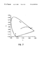
FIG. 7 is a view of the position of the color coordinates of the red, green and blue color filter elements according to Examples 1 and 2.
FIG. 8 is a view of the spectral transmission course on the red, green, and blue color filter elements on the filter system of the present invention according to Example 1;
FIG. 9 is a view of the course similar to FIG. 8 for the color filter elements on the filter system of the is present invention but according to Example 2; and
FIG. 10 is a schematic view of the manufacturing sequence of an interference filter system of the invention according to FIG. 2 or FIG. 3 but, particularly FIG. 4, according to the present invention.
DETAILED DESCRIPTION OF THE DRAWINGS
FIG. 1, which illustrates a known LCD-structure and has been described in detail above, shows, in a greatly exaggerated manner, the thickness differences for dielectric interference color filter elements 3.
FIG. 2 shows schematically the arrangement of the filter elements 3 above the substrate 1, according to the present invention, particularly for a red, green and blue transmission. With the exception of the unavoidable manufacturing tolerance of the individual layers (not shown), the number and the thickness of the layers are optimized such that all filter elements 3 e have the same thickness do. This optimization can optionally include the spectral characteristics of the substrate 1 as well as of additional layers (not shown) which can also be provided to cover the filter elements 3 e for optimization of the respective spectral filter element characteristics. Depending on the purpose of the filter system according to the present invention with the dielectric interference filter elements 3 e of the same height, as illustrated schematically in FIG. 2, black matrix elements 5 may be provided below, between or above the filter elements 3 e.
FIG. 3 shows a second embodiment which, by itself, is essential to the present invention, on the filter system with dielectric interference filter elements 3 f according to the present invention. Whereas the filter elements 3 in FIGS. 1 and 2 set gaps between one another, the filter elements 3 f in FIG. 3 adjoin one another without gaps, i.e. abut one another. As illustrated, black matrix elements 5 may also be built in, depending on the end use or application.
In the currently preferred embodiment according to FIG. 4, the respective inventive features of an interference filter system are combined. Therefore, the filter elements 3 ef, on one hand, have the same thicknesses as in FIG. 2; while, on the other hand, they adjoin one another without gaps as in FIG. 3. As illustrated in FIG. 4, it is therefore now possible to deposit a layer system or a layer of a constant thickness directly on the filter elements 3 ef, particularly, for example, an electrically conductive ITO-layer. In this embodiment, the color filter elements 3 ef form a mechanically stable reference plane of the construction of layer 15, and also form an electrically insulating depositing surface. Consequently, the layer 15 can be built up with a constant thickness, particularly if, as in the case of LCD-applications, their free surface 15 o must be situated on a well-defined parallel plane with respect to the substrate 1.
As discussed above, when the filter system according to the present invention is used as a color filter system for LCDs, an additional organic compensation layer 9 of FIG. 1 will not be necessary because an electrically conductive layer, particularly an ITO-layer or a layer stack made, for example, of SiO2/ITO, due to the good adhesion to dielectric layer systems, can be applied without any problems directly to the filter elements. Also, the applied, electrically conductive layer within the active filter system range will not encounter edges on the filter elements on which it could tear off, and the electrically conductive layer is insulated with respect to the black matrix elements disposed under the filter elements by the filter elements themselves.
EXAMPLE 1
The construction of an LCD-display according to the invention with the use of a color filter system according to FIG. 4 of the invention is schematically shown in FIG. 5. The color filter elements 3 ef and, above them, the electrically conductive ITO-layer 15 are situated on the substrate 1. The ITO-layer 15 is followed by the liquid crystal layer 10, the electrically conductive ITO-layer 13, and the substrate 11.
Together with the ITO-layer 15, the layer stacks of the color filter elements 3 ef in FIG. 5 each form an interference-capable system, which is why the ITO-layer must be taken into account during the optimization of the respective color filter elements to prevent an additional transmission loss occurring as a result of the ITO-layer.
First, the target values for the color coordinates of the R-, G- and B-filter elements are determined. In this example, these are the color coordinates for color television according to the E.B.U. D 28-1980 (E) Standard “The Chromaticity of the Luminophors of Television Receivers”.
Then, a thin-film system consisting of SiO2 (n=1.46; k=0) and TiO2 (n350 nm=2.55, n550 nm=2.35, n900 nm −2.22; k=0) is optimized such that the blue color coordinates are reached within a predetermined tolerance. In this case,
nsubstrat=1.52
nITO=2
dITO=110 nm
nLC−1.52
Absorption for all optical layers is assumed to be negligible. Then the green and red filter element layer systems are similarly optimized such that the corresponding color coordinates are reached within predetermined tolerances and the overall thickness becomes identical in each case to that of the blue filter element layer system. Table 1 shows under Example 1 the resulting color coordinate values and the layer construction of the “red”, “green” and “blue” filter elements. The resulting overall thickness of the color filter elements corresponds to ±0.2 nm.
FIG. 7 shows the resulting color coordinate values. FIG. 8 shows the spectral characteristics of the color filter elements implemented according to Example 1, including the substrate, the ITO-layers and the LC-layer.
EXAMPLE 2
FIG. 6 illustrates schematically the construction of a second embodiment of an LCD-screen with the filter system according to the present invention. The same reference numbers are used as in FIG. 5 to designate similar elements. With respect to the construction according to FIG. 5 and Example 1, however, a compensation layer 9 is provided in the embodiment of FIG. 6 between the filter elements 3 ef of the optical filter system and the ITO-layer 15. Thereby, the ITO-layer acts as an individual insulating layer. That is, in parts of the visible spectrum, the ITO-layer 15 reduces the transmission without compensation by the color filter elements 3 ef. The process for determining target values and optimizing is identical with that of Example 1. np=1.46 is assumed for the
| TABLE 1 |
| |
| Result of Thin Film Optimization from Examples 1 and 2; |
| H . . . TiO2-Layers, L . . . SiO2-Layers |
| |
Red |
Green |
Blue |
Red |
Green |
Blue |
| |
|
| Color |
|
x: |
0.647 |
0.317 |
0.141 |
0.653 |
0.317 |
0.141 |
| Coordinates: |
|
y: |
0.350 |
0.598 |
0.061 |
0.346 |
0.598 |
0.061 |
| |
|
Y: |
17.4% |
61.6% |
5.4% |
15.6% |
61.6% |
5.4% |
| Layer |
1 |
L |
19.0 |
0.0 |
0.0 |
0.0 |
0.0 |
0.0 |
| Construction |
2 |
H |
24.9 |
43.0 |
77.2 |
24.9 |
43.5 |
77.2 |
| (Thicknesses |
3 |
L |
69.6 |
33.0 |
98.0 |
69.6 |
33.3 |
98.0 |
| in nm): |
4 |
H |
43.0 |
38.5 |
63.2 |
43.0 |
38.9 |
63.2 |
| |
5 |
L |
69.6 |
95.3 |
105.4 |
69.6 |
96.2 |
105.4 |
| |
6 |
H |
43.0 |
40.7 |
56.2 |
43.0 |
41.2 |
56.2 |
| |
7 |
L |
51.3 |
66.0 |
105.4 |
51.3 |
66.6 |
105.4 |
| |
8 |
H |
38.5 |
40.7 |
56.2 |
38.5 |
41.2 |
56.2 |
| |
9 |
L |
69.6 |
66.0 |
105.4 |
69.6 |
66.6 |
105.4 |
| |
10 |
H |
43.0 |
40.7 |
56.2 |
43.0 |
41.2 |
56.2 |
| |
11 |
L |
69.6 |
66.0 |
105.4 |
69.6 |
66.6 |
105.4 |
| |
12 |
H |
45.2 |
56.6 |
56.2 |
45.2 |
50.3 |
56.2 |
| |
13 |
L |
66.0 |
58.6 |
105.4 |
66.0 |
70.3 |
105.4 |
| |
14 |
H |
43.0 |
43.0 |
58.5 |
43.0 |
34.3 |
58.5 |
| |
15 |
L |
40.3 |
183.2 |
101.7 |
40.3 |
188.6 |
101.7 |
| |
16 |
H |
52.0 |
70.1 |
67.9 |
52.0 |
70.9 |
67.9 |
| |
17 |
L |
69.6 |
117.2 |
98.0 |
69.6 |
118.3 |
98.0 |
| |
18 |
H |
58.8 |
70.1 |
77.2 |
58.8 |
70.9 |
77.2 |
| |
19 |
L |
62.3 |
117.2 |
116.7 |
62.3 |
118.3 |
116.7 |
| |
20 |
H |
58.8 |
70.1 |
77.2 |
58.8 |
70.9 |
77.2 |
| |
21 |
L |
69.6 |
117.2 |
116.7 |
69.6 |
118.3 |
116.7 |
| |
22 |
H |
72.4 |
70.1 |
77.2 |
72.4 |
70.9 |
77.2 |
| |
23 |
L |
58.6 |
117.2 |
116.7 |
69.6 |
118.3 |
116.7 |
| |
24 |
H |
65.6 |
70.1 |
79.6 |
65.6 |
70.9 |
77.2 |
| |
25 |
L |
69.6 |
117.2 |
98.0 |
58.6 |
118.3 |
116.7 |
| |
26 |
H |
70.1 |
95.0 |
|
65.6 |
89.2 |
79.6 |
| |
27 |
L |
69.6 |
58.6 |
|
69.6 |
92.5 |
| |
28 |
H |
63.3 |
113.1 |
|
70.1 |
105.2 |
| |
29 |
L |
55.0 |
|
|
69.6 |
59.2 |
| |
30 |
H |
65.6 |
|
|
63.3 |
| |
31 |
L |
73.3 |
|
|
55.0 |
| |
32 |
H |
52.0 |
|
|
65.6 |
| |
33 |
L |
252.8 |
|
|
73.3 |
| |
34 |
H |
|
|
|
67.9 |
| |
35 |
L |
|
|
|
44.0 |
| |
36 |
H |
|
|
|
40.7 |
| |
37 |
L |
|
|
|
131.9 |
| Overall thickness: |
|
|
2074.8 |
2074.5 |
2075.4 |
2170.6 |
2170.9 |
2171.4 |
| |
compensation layer. FIGS. 7 and 9 of the table again show the result of such an optimization. Table 1 illustrates that the overall thicknesses of the color filter elements coincide to deviations of less than 1 nm, specifically to ±0.25 nm.
EXAMPLE 3
With respect to FIG. 10, the manufacturing process according to the present invention, will be explained by reference to the following eight steps
Step 1
The substrate is coated with the first interference filter system B, particularly with a first color filter system, such as blue “B”.
Step 2
An etching mask 17, for example, a chromium mask, is applied to the deposited layer system, for example, by lithography or the like.
Step 3
The applied layer system B is structured by etching, preferably by reactive ion etching, such that the first filter elements of the first spectral characteristic, here for the example, the blue color “B” filter elements, are prepared.
Step 4
While the etching mask 17 remains, coating of the second spectral characteristic, here for example, with the green “G” layer system on the etching mask 17 and on the substrate, takes place.
Step 5
A second etching mask 19 again, for example, a chromium etching mask, is applied to the green color “G” layer system by lithography or other acceptable process.
Step 6
By way of etching, the second filter elements of the second spectral characteristic, such as the green color “G” filter elements, are prepared. The etching is again preferably carried out by means of reactive ion etching.
Step 7
While the first and second etching masks 17 and 19 remain, coating is carried out by the third layer system corresponding to the desired third spectral characteristic, such as the red “R” characteristic As a result, all gaps are closed between the already applied filter elements B, G.
Step 8
By use of the lift-off technique, the last-applied layer system is structured, in which case the previously used etching masks 17, 19 are now used as lift-off masks which are removed.
Although the invention has been described and illustrated in detail, it is to be clearly understood that the same is by way of illustration and example, and is not to be taken by way of limitation. The spirit and scope of the present invention are to be limited only by the terms of the appended claims.