US6340109B2 - Solder bump measuring method and apparatus - Google Patents
Solder bump measuring method and apparatus Download PDFInfo
- Publication number
- US6340109B2 US6340109B2 US09/755,106 US75510601A US6340109B2 US 6340109 B2 US6340109 B2 US 6340109B2 US 75510601 A US75510601 A US 75510601A US 6340109 B2 US6340109 B2 US 6340109B2
- Authority
- US
- United States
- Prior art keywords
- work
- solder bump
- bump
- bumps
- measuring
- Prior art date
- Legal status (The legal status is an assumption and is not a legal conclusion. Google has not performed a legal analysis and makes no representation as to the accuracy of the status listed.)
- Expired - Fee Related
Links
Images


Classifications
-
- G—PHYSICS
- G01—MEASURING; TESTING
- G01B—MEASURING LENGTH, THICKNESS OR SIMILAR LINEAR DIMENSIONS; MEASURING ANGLES; MEASURING AREAS; MEASURING IRREGULARITIES OF SURFACES OR CONTOURS
- G01B11/00—Measuring arrangements characterised by the use of optical techniques
- G01B11/02—Measuring arrangements characterised by the use of optical techniques for measuring length, width or thickness
- G01B11/06—Measuring arrangements characterised by the use of optical techniques for measuring length, width or thickness for measuring thickness ; e.g. of sheet material
- G01B11/0608—Height gauges
-
- H—ELECTRICITY
- H05—ELECTRIC TECHNIQUES NOT OTHERWISE PROVIDED FOR
- H05K—PRINTED CIRCUITS; CASINGS OR CONSTRUCTIONAL DETAILS OF ELECTRIC APPARATUS; MANUFACTURE OF ASSEMBLAGES OF ELECTRICAL COMPONENTS
- H05K13/00—Apparatus or processes specially adapted for manufacturing or adjusting assemblages of electric components
- H05K13/08—Monitoring manufacture of assemblages
- H05K13/081—Integration of optical monitoring devices in assembly lines; Processes using optical monitoring devices specially adapted for controlling devices or machines in assembly lines
- H05K13/0813—Controlling of single components prior to mounting, e.g. orientation, component geometry
-
- H—ELECTRICITY
- H01—ELECTRIC ELEMENTS
- H01L—SEMICONDUCTOR DEVICES NOT COVERED BY CLASS H10
- H01L22/00—Testing or measuring during manufacture or treatment; Reliability measurements, i.e. testing of parts without further processing to modify the parts as such; Structural arrangements therefor
- H01L22/10—Measuring as part of the manufacturing process
- H01L22/12—Measuring as part of the manufacturing process for structural parameters, e.g. thickness, line width, refractive index, temperature, warp, bond strength, defects, optical inspection, electrical measurement of structural dimensions, metallurgic measurement of diffusions
Definitions
- the present invention relates to a method and apparatus for measuring solder bumps formed on a semiconductor module such as LSI, on TAB (Tape Automated Bonding), and the like.
- FIGS. 1A to 1 C illustrate the structure of a semiconductor module 1 having a number of solder bumps.
- FIG. 1A is a diagram showing the overall structure of the semiconductor module.
- FIG. 1B is an enlarged view of a bump area A of the semiconductor module and illustrates a relative position of solder bumps.
- FIG. 1C is an enlarged view of a bump 10 (corresponding to B in FIG. 1 A).
- solder bumps 10 are formed on the bottom of the semiconductor module 1 . Each bump is used for connection to a wiring board on which the semiconductor module 1 is mounted.
- the semiconductor module 1 is of a square shape having a side length of, for example, 10 mm.
- Solder bumps 10 are formed on the surface 8 at a pitch of, for example, 450 ⁇ m, totalling in number to 23 ⁇ 23.
- Each bump 10 is generally spherical as shown in the enlarged view of FIG. 1 C.
- the size of each bump is required to have predetermined values so that adjacent bumps and wiring connections are prevented from being electrically shorted.
- One of the inventors of this invention has proposed techniques of measuring a height of a work by using an optical beam, as disclosed in JP-A-2-80905.
- the measuring method of this invention comprises the steps of: mounting a work to be measured on a table, the work having solder bump rows; detecting a reference bump from the solder bumps by using a laser optical micro head; scanning the solder bump rows with the optical micro head and detecting a shift amount of a mount posture of the work; correcting the shift amount of the mount posture of the work by scanning the table; and measuring height positions of apexes of all the solder bumps with the optical micro head.
- the method of the invention further comprises the steps of calculating a regression plane formed by the apexes of the solder bumps and calculating a relative apex position of each solder bump relative to the calculated regression plane.
- the method of the invention further comprises the steps of calculating a standard deviation of relative heights and judging from the standard deviation and the apex height of each bump whether the work is defective or not.
- a measure apparatus of this invention comprises: a table for placing thereon a work to be measured, the work having solder bump rows; moving means for moving the table in a two-dimensional plane in two perpendicular axis directions; rotating means for rotating the table about a vertical axis; inclining means for inclining the table; a laser optical micro head mounted on the table to be movable in the vertical axis direction; a personal computer for recording data measured by the optical micro head in the form of digital data; controlling means for controlling the table and the optical micro head; a personal computer for calculating a height position of an apex of each solder bump in accordance with the data measured by the optical micro head; a display screen for displaying the calculated results; and a printer for printing out the calculated results.
- a work is measured by scanning a light spot by the optical micro head. Therefore, the drive speed can be changed depending upon a necessary measurement precision and the size of the work, so that high speed, high precision, and versatility can be realized for various applications.
- the invention provides a method and apparatus for measuring heights of all of a number of bumps formed on a work such as an LSI and judging whether the work is good or not.
- the invention is applicable to works having highly dense bumps expected in the future.
- FIG. 1A illustrates a semiconductor module used as a work to be measured
- FIGS. 1B and 1C are enlarged views showing bumps and a bump on the semiconductor module.
- FIG. 2 is a perspective view of a measuring apparatus of this invention.
- FIG. 3 is a block diagram showing the structure of the measuring apparatus of the invention.
- FIG. 4 is a perspective view showing the structure of an optical micro head.
- FIG. 5 is a plan view illustrating scanning of an optical micro head.
- FIG. 6 is a diagram showing an example of measurement results.
- FIGS. 7A and 7B are diagrams illustrating a method of measuring the apex of a solder bump on a substrate surface.
- FIG. 8 is a diagram illustrating the effects of swell of a substrate.
- FIG. 9 is a plan view illustrating a mount of a work on a work table.
- FIG. 10 is a plan view illustrating a method of detecting a bump apex position.
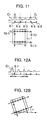
- FIG. 11 is a diagram illustrating measurement results with substrate mount errors.
- FIG. 12A is a diagram illustrating measurement results with substrate mount errors
- FIG. 12B is a diagram illustrating rotation correction of mount errors.
- FIG. 13 is a diagram illustrating measurement results with substrate mount errors.
- FIG. 14 is a diagram illustrating a regression plane of apexes of solder bumps.
- FIG. 15 is a graph showing a standard deviation of measurement results.
- FIG. 16 is a diagram illustrating a display screen of a monitor.
- FIG. 2 is a diagram showing an apparatus used with a solder bump measuring method of this invention.
- This measuring apparatus generally indicated by reference numeral 100 has an operation stage 105 on which a work is placed and measured, a control unit 120 , an operation panel 130 , a printer 140 for outputting measurement results, a monitor TV for monitoring a measurement area of the operation stage 105 , and the like.
- FIG. 3 is a block diagram showing the control system of the measuring apparatus 100 shown in FIG. 2.
- a table frame on which a work 1 is placed is mounted on an anti-vibration base 210 .
- the table frame has a ⁇ stage 212 for controlling an angle around the work vertical axis (Z axis), an X stage 214 for controlling a motion in a guide axis (X axis) in the plane perpendicular to the vertical axis, a Y stage 214 for controlling a motion in a guide axis (Y axis) perpendicular to the X axis, and a ⁇ inclination stage 218 and an ⁇ inclination stage 220 respectively for controlling inclination of the surface of a work positioning mechanism (work table) 230 .
- Each control axis is controlled by outputs from an axis controller/driver apparatus 240 .
- An optical microsensor 250 is mounted on a Z axis driver mechanism 270 and is used for controlling the optical microsensor in the Z axis relative to the work table 230 .
- This optical microsensor 250 can be retracted away from a measuring position of the work table 230 by a retracting mechanism 272 so that the work 1 can be easily placed on or dismounted from the operation stage.
- a motion amount in the Z axis is measured by a digital micrometer 274 .
- An optical camera 252 is mounted at the side of the optical microsensor 250 , and the state of the measuring area can be monitored by a CRT 150 .
- the optical microsensor 250 is controlled by a controller 260 , and the measured data is A/D converted and supplied via a digital input/output interface 264 to a computing apparatus, for example, a personal computer 266 .
- the measurement results are supplied via a digital input/output interface 280 to a computing apparatus, for example, a master personal computer 110 .
- the measurement results are displayed on the personal computer 110 and printed out from a printer 140 .
- the measurement results of solder bumps are judged in accordance with coordinate data of each bump position and correction amount data of each control axis, by using an operation switch 284 .
- FIG. 4 shows the structure of the optical micro head 250 which has a semiconductor laser 252 and a light receiving element 255 .
- a laser beam radiated from the semiconductor laser 252 passes through a lens 253 and applied to a bump 10 as a laser beam LB.
- the laser beam reflected at the surface of the bump 10 passes through a lens 254 and is received by the light receiving element 255 .
- the light receiving element 255 measures the height position of the bump surface in accordance with a position where the reflected light is received, by using the principle of triangulation, and also detects the amount of reflected light.
- the X axis of the table is aligned with the optical axis of the laser beam LB.
- FIG. 5 shows scan paths along which the bump 10 is scanned with the laser beam LB.
- the surface area including the apex of the bump 10 is measured by three paths. Three paths are used for obtaining a correct value while considering the position displacement of each bump. Three paths are only illustrative and a plurality of paths may be set depending upon the measurement conditions.
- FIG. 6 shows an example of the measurement results wherein the abscissa represents the X axis and the ordinate represents a detected level.
- a first curve C 1 indicates a level of reflected and received light, and a second curve C 2 indicates a change in height of the bump.
- a reference value TL of the level of the reflected and received light C 1 is preset.
- An X axis position where the received light becomes larger than the reference value TL and an X axis position where the received light becomes smaller than the reference value are detected.
- the value of the height signal C 2 at the middle coordinate position X 10 is used as the height of the apex of the bump.
- FIGS. 7A and 7B illustrate a relationship between the surface 8 of the substrate 2 and the height position of the bump 10 .
- the laser beam LB scans the surface 8 of the substrate 2 and the bump 10 to detect the height positions of the surface 8 and bump 10 .
- the substrate is not always absolutely flat, since it may have a swell or the like. Therefore, as shown in FIG. 8, a regression plane P 1 of the surface 8 of the substrate 8 and a regression plane P 2 of the apexes of bumps are calculated.
- the regression plane means a virtual plane which minimizes the distances to bumps. This is the same concept as a regression line. It is more effective from the viewpoint of process to evaluate the bump height from the distance to the regression plane than using the absolute bump height.
- FIG. 9 shows a positioning device for positioning an LSI carrier as a work on the work table 230 which moves in X and Y directions.
- a work 1 is of a square shape.
- a right angle block 232 conformal to the work 1 is mounted on the table 230 .
- the block 232 has reference stoppers 233 .
- the work 1 is pushed against the stoppers 233 by a pushing pin 234 which moves toward the stoppers 233 .
- the table 230 has a suction device 235 which uses a negative pressure to suck the bottom of the work 1 .
- the controller knows in advance the position, as designed, of the first bump 10 - 1 relative to the substrate of the work 1 . Therefore, first, the coordinates of the X axis of the table are aligned with the design coordinates of the first bump 10 - 1 , and a first scan S- 1 is performed for measurement while moving the table in the Y direction.
- a curve indicating a change in the amount of reflected and received light of the first bump 10 - 1 such as the curve C 1 shown in FIG. 6, can be obtained.
- the center position of the light amount of this curve is obtained, this position being assumed as the center (origin) of the first bump 10 - 1 . If the received light amount does not exceed the reference value, the X axis coordinates are shifted by a distance D 1 to execute a second scan S- 2 to detect the temporary origin and determine the Y axis coordinates.
- a scan S- 3 is performed in the X axis direction to determine the position of the first bump 10 - 1 from the center of the received light amount. If the received light amount does not exceed the reference value at the X axis coordinates, the Y axis coordinates are shifted by a distance D 2 to execute a scan S- 4 to perform similar operations as above.
- the coordinate values obtained in the above manner are used as a temporary origin K 1 .
- a first row of bumps including the temporary origin K 1 is scanned (S- 10 ), and the apex positions of bumps are obtained which show a received light amount in excess of the reference value.
- An average value of shift amounts between the X axis coordinates of apex positions and the designed X axis coordinates is calculated (refer to FIG. 11 ).
- a correction value of a distance from the end of the work substrate to the first bump in the X axis direction is determined to correct the X axis coordinates of the origin.
- Similar scans are executed in the Y axis direction to calculate the shift amounts of the Y axis coordinates and correct the Y axis coordinates of the origin.
- the peak values of the received light amount on the scan line change in a predetermined direction and a shift occurs between the peak position and the design position (refer to FIG. 12 A).
- a correction value for the work rotation angle ⁇ is calculated to rotate the ⁇ stage and correct its position (refer to FIG. 12 B).
- a scan for the ⁇ correction is executed in the X axis direction
- the heights at positions 8 - 1 , 8 - 2 , 8 - 3 , . . . on the work substrate are also detected (refer to FIG. 8 ).
- a regression line L- 1 is calculated and a correction value ⁇ for an inclination angle from the reference line (horizontal line) in the X axis direction is calculated to correct the ⁇ inclination stage 220 .
- a correction value ⁇ for an inclination angle in the Y axis direction is calculated to correct the ⁇ inclination stage 218 .
- a measuring laser beam can be scanned highly precisely at high speed. Therefore, the bump heights can be measured highly precisely at high speed.
- FIG. 14 shows a regression plane PL- 1 formed by the measured apex positions of bumps 10 .
- a shift of each bump apex position is calculated from this regression plane PL- 1 and the judgement results are displayed on the display 112 .
- FIG. 15 is a graph showing the measurement results displayed on the screen.
- the abscissa represents a difference between each bump apex and the regression plane, and the ordinate represents the number of bumps.
- This work has 5200 bumps, the standard deviation is 0.5 ⁇ m, and 3 ⁇ is ⁇ 1.95 ⁇ m.
- a target value is set to +/ ⁇ 2 ⁇ m
- the work is judged good from the standard deviation, and is transported to the next process.
- the work may be judged good to transport it to the next process, if all bumps are in a range of predetermined reference values.
- FIG. 16 shows examples of various displays displayed on the screen 112 of the measuring apparatus.
- An operation screen 300 has a display area 302 for a present operation mode and the like, an area 304 for displaying a relative height occurrence frequency distribution graph, an area 306 for displaying judgement results, and an area 308 for displaying the detailed results for each LSI as a work.
- the position of a defective bump 10 -N of the work 1 is displayed with graphics.
- the relative height occurrence frequency distribution graph 304 is shown in FIG. 15 .
- the judgement results are displayed in the area 306 by OK or NG.
- the alignment results are displayed by values of X, Y, Z, ⁇ , ⁇ , and ⁇ , and also a bump average height, standard deviation of relative heights, received light average amount, and base shrinkage ratios in X and Y directions are displayed.
- a position shift graph screen 310 shows a distribution of a shift amount of an apex position from a design value for each bump.
- a height three-dimensional distribution graph screen 320 shows a 3D graph of relative heights of respective bumps and a two-dimensional distribution graph in different colors.
- a defective LSI information graph screen 330 shows a judgement mode of a defective LSI after full automatic operation (in units of magazine).
- An inspection condition setting screen 340 is used for setting inspection parameters such as judgement threshold values.
- an operation speed of 32 mm/sec, optical micro head frequency of 16 kHz, measurement resolution in the horizontal direction of 2 to 3 ⁇ m, and measurement resolution in the height direction (Z direction) of 0.05 ⁇ m can be realized.
Abstract
A work having a number of solder bumps on a substrate is mounted on a work positioning mechanism, and scanned by an optical micro head to measure errors of a mount posture of the work. Each stage is controlled to correct the errors, and thereafter, the apex positions of the bumps are scanned and measured. The measurement results are collected by a personal computer, and the measurement results together with control data of each axis are sent to a main personal computer and displayed on its screen. An error of an apex position of each bump from a regression plane is calculated, and if the error is smaller than a reference value, the work is judged to be good.
Description
This is a divisional application of U.S. Ser. No. 09/289,386, filed Apr. 12, 1999 now U.S. Pat. No. 6,196,441, issued Mar. 6, 2001.
1. Field of the Invention
The present invention relates to a method and apparatus for measuring solder bumps formed on a semiconductor module such as LSI, on TAB (Tape Automated Bonding), and the like.
2. Description of the Related Art
FIGS. 1A to 1C illustrate the structure of a semiconductor module 1 having a number of solder bumps. FIG. 1A is a diagram showing the overall structure of the semiconductor module. FIG. 1B is an enlarged view of a bump area A of the semiconductor module and illustrates a relative position of solder bumps. FIG. 1C is an enlarged view of a bump 10 (corresponding to B in FIG. 1A).
A number of solder bumps 10 are formed on the bottom of the semiconductor module 1. Each bump is used for connection to a wiring board on which the semiconductor module 1 is mounted. The semiconductor module 1 is of a square shape having a side length of, for example, 10 mm. Solder bumps 10 are formed on the surface 8 at a pitch of, for example, 450 μm, totalling in number to 23×23.
Each bump 10 is generally spherical as shown in the enlarged view of FIG. 1C.
There is no apparatus for automatically measuring a height of a number of spherical bumps to date. Therefore, height is measured visually by using a focus-of-depth microscope or the like.
Works (to be measured) such as semiconductor modules formed with a number of bumps are positioned at a later process on a wiring board, and bumps are heated and melted in a heating furnace to be connected to the wiring board.
In order to reliably connect the bumps, it is necessary to correctly measure a height of each bump at its apex.
The size of each bump is required to have predetermined values so that adjacent bumps and wiring connections are prevented from being electrically shorted.
However, it is very difficult to measure heights of a number of bumps correctly and in a short time.
One of the inventors of this invention has proposed techniques of measuring a height of a work by using an optical beam, as disclosed in JP-A-2-80905.
It is an object of the present invention to provide a method and apparatus capable of measuring bumps on a work correctly at high speed.
The measuring method of this invention comprises the steps of: mounting a work to be measured on a table, the work having solder bump rows; detecting a reference bump from the solder bumps by using a laser optical micro head; scanning the solder bump rows with the optical micro head and detecting a shift amount of a mount posture of the work; correcting the shift amount of the mount posture of the work by scanning the table; and measuring height positions of apexes of all the solder bumps with the optical micro head.
The method of the invention further comprises the steps of calculating a regression plane formed by the apexes of the solder bumps and calculating a relative apex position of each solder bump relative to the calculated regression plane. The method of the invention further comprises the steps of calculating a standard deviation of relative heights and judging from the standard deviation and the apex height of each bump whether the work is defective or not.
A measure apparatus of this invention comprises: a table for placing thereon a work to be measured, the work having solder bump rows; moving means for moving the table in a two-dimensional plane in two perpendicular axis directions; rotating means for rotating the table about a vertical axis; inclining means for inclining the table; a laser optical micro head mounted on the table to be movable in the vertical axis direction; a personal computer for recording data measured by the optical micro head in the form of digital data; controlling means for controlling the table and the optical micro head; a personal computer for calculating a height position of an apex of each solder bump in accordance with the data measured by the optical micro head; a display screen for displaying the calculated results; and a printer for printing out the calculated results.
According to the present invention, a work is measured by scanning a light spot by the optical micro head. Therefore, the drive speed can be changed depending upon a necessary measurement precision and the size of the work, so that high speed, high precision, and versatility can be realized for various applications.
As above, the invention provides a method and apparatus for measuring heights of all of a number of bumps formed on a work such as an LSI and judging whether the work is good or not. The invention is applicable to works having highly dense bumps expected in the future.
FIG. 1A illustrates a semiconductor module used as a work to be measured, and FIGS. 1B and 1C are enlarged views showing bumps and a bump on the semiconductor module.
FIG. 2 is a perspective view of a measuring apparatus of this invention.
FIG. 3 is a block diagram showing the structure of the measuring apparatus of the invention.
FIG. 4 is a perspective view showing the structure of an optical micro head.
FIG. 5 is a plan view illustrating scanning of an optical micro head.
FIG. 6 is a diagram showing an example of measurement results.
FIGS. 7A and 7B are diagrams illustrating a method of measuring the apex of a solder bump on a substrate surface.
FIG. 8 is a diagram illustrating the effects of swell of a substrate.
FIG. 9 is a plan view illustrating a mount of a work on a work table.
FIG. 10 is a plan view illustrating a method of detecting a bump apex position.
FIG. 11 is a diagram illustrating measurement results with substrate mount errors.
FIG. 12A is a diagram illustrating measurement results with substrate mount errors, and FIG. 12B is a diagram illustrating rotation correction of mount errors.
FIG. 13 is a diagram illustrating measurement results with substrate mount errors.
FIG. 14 is a diagram illustrating a regression plane of apexes of solder bumps.
FIG. 15 is a graph showing a standard deviation of measurement results.
FIG. 16 is a diagram illustrating a display screen of a monitor.
FIG. 2 is a diagram showing an apparatus used with a solder bump measuring method of this invention.
This measuring apparatus generally indicated by reference numeral 100 has an operation stage 105 on which a work is placed and measured, a control unit 120, an operation panel 130, a printer 140 for outputting measurement results, a monitor TV for monitoring a measurement area of the operation stage 105, and the like.
FIG. 3 is a block diagram showing the control system of the measuring apparatus 100 shown in FIG. 2. A table frame on which a work 1 is placed is mounted on an anti-vibration base 210. The table frame has a θ stage 212 for controlling an angle around the work vertical axis (Z axis), an X stage 214 for controlling a motion in a guide axis (X axis) in the plane perpendicular to the vertical axis, a Y stage 214 for controlling a motion in a guide axis (Y axis) perpendicular to the X axis, and a β inclination stage 218 and an α inclination stage 220 respectively for controlling inclination of the surface of a work positioning mechanism (work table) 230.
Each control axis is controlled by outputs from an axis controller/driver apparatus 240.
An optical microsensor 250 is mounted on a Z axis driver mechanism 270 and is used for controlling the optical microsensor in the Z axis relative to the work table 230. This optical microsensor 250 can be retracted away from a measuring position of the work table 230 by a retracting mechanism 272 so that the work 1 can be easily placed on or dismounted from the operation stage. A motion amount in the Z axis is measured by a digital micrometer 274.
An optical camera 252 is mounted at the side of the optical microsensor 250, and the state of the measuring area can be monitored by a CRT 150.
The optical microsensor 250 is controlled by a controller 260, and the measured data is A/D converted and supplied via a digital input/output interface 264 to a computing apparatus, for example, a personal computer 266.
The measurement results are supplied via a digital input/output interface 280 to a computing apparatus, for example, a master personal computer 110. The measurement results are displayed on the personal computer 110 and printed out from a printer 140.
The measurement results of solder bumps are judged in accordance with coordinate data of each bump position and correction amount data of each control axis, by using an operation switch 284.
FIG. 4 shows the structure of the optical micro head 250 which has a semiconductor laser 252 and a light receiving element 255. A laser beam radiated from the semiconductor laser 252 passes through a lens 253 and applied to a bump 10 as a laser beam LB. The laser beam reflected at the surface of the bump 10 passes through a lens 254 and is received by the light receiving element 255. The light receiving element 255 measures the height position of the bump surface in accordance with a position where the reflected light is received, by using the principle of triangulation, and also detects the amount of reflected light.
The X axis of the table is aligned with the optical axis of the laser beam LB.
FIG. 5 shows scan paths along which the bump 10 is scanned with the laser beam LB. The surface area including the apex of the bump 10 is measured by three paths. Three paths are used for obtaining a correct value while considering the position displacement of each bump. Three paths are only illustrative and a plurality of paths may be set depending upon the measurement conditions.
FIG. 6 shows an example of the measurement results wherein the abscissa represents the X axis and the ordinate represents a detected level. A first curve C1 indicates a level of reflected and received light, and a second curve C2 indicates a change in height of the bump.
A reference value TL of the level of the reflected and received light C1 is preset. An X axis position where the received light becomes larger than the reference value TL and an X axis position where the received light becomes smaller than the reference value are detected. The value of the height signal C2 at the middle coordinate position X10 is used as the height of the apex of the bump.
FIGS. 7A and 7B illustrate a relationship between the surface 8 of the substrate 2 and the height position of the bump 10.
The laser beam LB scans the surface 8 of the substrate 2 and the bump 10 to detect the height positions of the surface 8 and bump 10.
The substrate is not always absolutely flat, since it may have a swell or the like. Therefore, as shown in FIG. 8, a regression plane P1 of the surface 8 of the substrate 8 and a regression plane P2 of the apexes of bumps are calculated.
An absolute height H1 from the regression plane P1 and a relative height H2 from the regression plane P2 are then obtained.
There is not always a constant relationship between the size and shape of the substrate of a work to be measured and the position of each solder bump on the substrate, because a work precision of the substrate has a limit. Therefore, after the work is placed on the table, the mount posture of the work is aligned before measurement.
The regression plane means a virtual plane which minimizes the distances to bumps. This is the same concept as a regression line. It is more effective from the viewpoint of process to evaluate the bump height from the distance to the regression plane than using the absolute bump height.
FIG. 9 shows a positioning device for positioning an LSI carrier as a work on the work table 230 which moves in X and Y directions.
A work 1 is of a square shape. A right angle block 232 conformal to the work 1 is mounted on the table 230. The block 232 has reference stoppers 233. The work 1 is pushed against the stoppers 233 by a pushing pin 234 which moves toward the stoppers 233.
The table 230 has a suction device 235 which uses a negative pressure to suck the bottom of the work 1.
There are some errors of the outer dimension of the LSI substrate and bump positions because of substrate scribe errors, shrinkage of substrate material, or the like.
For this reason, a process of detecting the position of a first bump 10-1 of the work 1 is executed as illustrated in FIG. 10.
The controller knows in advance the position, as designed, of the first bump 10-1 relative to the substrate of the work 1. Therefore, first, the coordinates of the X axis of the table are aligned with the design coordinates of the first bump 10-1, and a first scan S-1 is performed for measurement while moving the table in the Y direction.
With this scan S-1, a curve indicating a change in the amount of reflected and received light of the first bump 10-1, such as the curve C1 shown in FIG. 6, can be obtained. The center position of the light amount of this curve is obtained, this position being assumed as the center (origin) of the first bump 10-1. If the received light amount does not exceed the reference value, the X axis coordinates are shifted by a distance D1 to execute a second scan S-2 to detect the temporary origin and determine the Y axis coordinates.
Next, after the Y axis coordinates are fixed, a scan S-3 is performed in the X axis direction to determine the position of the first bump 10-1 from the center of the received light amount. If the received light amount does not exceed the reference value at the X axis coordinates, the Y axis coordinates are shifted by a distance D2 to execute a scan S-4 to perform similar operations as above.
The coordinate values obtained in the above manner are used as a temporary origin K1.
A first row of bumps including the temporary origin K1 is scanned (S-10), and the apex positions of bumps are obtained which show a received light amount in excess of the reference value. An average value of shift amounts between the X axis coordinates of apex positions and the designed X axis coordinates is calculated (refer to FIG. 11).
Next, a similar scan (S-11) is performed for the bump row remotest from he above bump row to thereby calculate an average value of shift amounts in the X axis coordinates.
In accordance with shift amounts, a correction value of a distance from the end of the work substrate to the first bump in the X axis direction is determined to correct the X axis coordinates of the origin.
Similar scans are executed in the Y axis direction to calculate the shift amounts of the Y axis coordinates and correct the Y axis coordinates of the origin.
If the work is mounted being rotated about the center axis and a scan is performed by shifting the scan position by a designed value, then the peak values of the received light amount on the scan line change in a predetermined direction and a shift occurs between the peak position and the design position (refer to FIG. 12A).
In accordance with this change, a correction value for the work rotation angle θ is calculated to rotate the θ stage and correct its position (refer to FIG. 12B).
While a scan for the θ correction is executed in the X axis direction, the heights at positions 8-1, 8-2, 8-3, . . . on the work substrate are also detected (refer to FIG. 8). In accordance with the change in the heights, a regression line L-1 is calculated and a correction value α for an inclination angle from the reference line (horizontal line) in the X axis direction is calculated to correct the α inclination stage 220.
Similarly, a correction value β for an inclination angle in the Y axis direction is calculated to correct the β inclination stage 218.
After the above alignment processes are completed, all bumps are scanned to measure the apex heights as already described with FIG. 5.
With precise alignment, a measuring laser beam can be scanned highly precisely at high speed. Therefore, the bump heights can be measured highly precisely at high speed.
FIG. 14 shows a regression plane PL-1 formed by the measured apex positions of bumps 10. A shift of each bump apex position is calculated from this regression plane PL-1 and the judgement results are displayed on the display 112.
FIG. 15 is a graph showing the measurement results displayed on the screen.
The abscissa represents a difference between each bump apex and the regression plane, and the ordinate represents the number of bumps.
This work has 5200 bumps, the standard deviation is 0.5 μm, and 3 δ is ±1.95 μm.
If a target value is set to +/−2 μm, the work is judged good from the standard deviation, and is transported to the next process. The work may be judged good to transport it to the next process, if all bumps are in a range of predetermined reference values.
FIG. 16 shows examples of various displays displayed on the screen 112 of the measuring apparatus.
An operation screen 300 has a display area 302 for a present operation mode and the like, an area 304 for displaying a relative height occurrence frequency distribution graph, an area 306 for displaying judgement results, and an area 308 for displaying the detailed results for each LSI as a work.
In the area 302, the following items are displayed.
(a) Present operation mode (alignment, apex measurement, base measurement, judgement calculation, second time individual measurement).
(b) Present inspection position (row, column) with graphics and values.
(c) Coordinates of defective bump of inspected LSI with graphics and values.
For the display of the position of a defective bump, for example, the position of a defective bump 10-N of the work 1 is displayed with graphics.
The relative height occurrence frequency distribution graph 304 is shown in FIG. 15. The judgement results are displayed in the area 306 by OK or NG. For the detailed results for each LSI in the area 308, the alignment results are displayed by values of X, Y, Z, θ, α, and β, and also a bump average height, standard deviation of relative heights, received light average amount, and base shrinkage ratios in X and Y directions are displayed.
A position shift graph screen 310 shows a distribution of a shift amount of an apex position from a design value for each bump.
A height three-dimensional distribution graph screen 320 shows a 3D graph of relative heights of respective bumps and a two-dimensional distribution graph in different colors.
A defective LSI information graph screen 330 shows a judgement mode of a defective LSI after full automatic operation (in units of magazine).
An inspection condition setting screen 340 is used for setting inspection parameters such as judgement threshold values.
With this invention, for example, an operation speed of 32 mm/sec, optical micro head frequency of 16 kHz, measurement resolution in the horizontal direction of 2 to 3 μm, and measurement resolution in the height direction (Z direction) of 0.05 μm, can be realized.
Claims (4)
1. A method of measuring solder bumps formed on a work to be measured, comprising the steps of
irradiating a light beam on each solder bump disposed on the work set on a table;
measuring an apex height of each solder bump by receiving a light reflected from each solder bump;
determining a regression plane constituted by said solder bumps by referring to said apex heights measured; and
determining a relative apex height of each solder bump relative to said determined regression plane.
2. A solder bump measuring method according to claim 1 , further comprising the steps of:
judging whether a relative apex height of each solder bump is within a predetermined value; and
displaying positions of solder bumps judged to be of inferior quality on display means.
3. A solder bump measuring method according to claim 1 , further comprising the steps of:
calculating a standard deviation regarding a relative apex height of each solder bump; and
judging whether the work is good or bad by referring to an apex height of each solder bump and said standard deviation.
4. A method of measuring solder bumps formed on a work to be measured, comprising the steps of:
irradiating a light beam on a surface of said work and a surface of each solder bump on said work set on a table;
measuring a height of said surface of said work and an apex height of each solder bump by receiving light reflected from said surface of said work and said surface of each solder bump of said work set on said table;
determining a regression plane constituted by said surface of said work from measured results; and
determining a relative apex height of each solder bump relative to said determined regression plane.
Priority Applications (1)
| Application Number | Priority Date | Filing Date | Title |
|---|---|---|---|
| US09/755,106 US6340109B2 (en) | 1995-12-05 | 2001-01-08 | Solder bump measuring method and apparatus |
Applications Claiming Priority (6)
| Application Number | Priority Date | Filing Date | Title |
|---|---|---|---|
| JP31628395A JP3335826B2 (en) | 1995-12-05 | 1995-12-05 | Solder bump measuring device |
| JP07-316283 | 1995-12-05 | ||
| JP7-316283 | 1995-12-05 | ||
| US08/759,949 US5906309A (en) | 1995-12-05 | 1996-12-03 | Solder bump measuring method and apparatus |
| US09/289,386 US6196441B1 (en) | 1995-12-05 | 1999-04-12 | Solder bump measuring method and apparatus |
| US09/755,106 US6340109B2 (en) | 1995-12-05 | 2001-01-08 | Solder bump measuring method and apparatus |
Related Parent Applications (1)
| Application Number | Title | Priority Date | Filing Date |
|---|---|---|---|
| US09/289,386 Division US6196441B1 (en) | 1995-12-05 | 1999-04-12 | Solder bump measuring method and apparatus |
Publications (2)
| Publication Number | Publication Date |
|---|---|
| US20010000904A1 US20010000904A1 (en) | 2001-05-10 |
| US6340109B2 true US6340109B2 (en) | 2002-01-22 |
Family
ID=18075388
Family Applications (3)
| Application Number | Title | Priority Date | Filing Date |
|---|---|---|---|
| US08/759,949 Expired - Fee Related US5906309A (en) | 1995-12-05 | 1996-12-03 | Solder bump measuring method and apparatus |
| US09/289,386 Expired - Fee Related US6196441B1 (en) | 1995-12-05 | 1999-04-12 | Solder bump measuring method and apparatus |
| US09/755,106 Expired - Fee Related US6340109B2 (en) | 1995-12-05 | 2001-01-08 | Solder bump measuring method and apparatus |
Family Applications Before (2)
| Application Number | Title | Priority Date | Filing Date |
|---|---|---|---|
| US08/759,949 Expired - Fee Related US5906309A (en) | 1995-12-05 | 1996-12-03 | Solder bump measuring method and apparatus |
| US09/289,386 Expired - Fee Related US6196441B1 (en) | 1995-12-05 | 1999-04-12 | Solder bump measuring method and apparatus |
Country Status (2)
| Country | Link |
|---|---|
| US (3) | US5906309A (en) |
| JP (1) | JP3335826B2 (en) |
Cited By (3)
| Publication number | Priority date | Publication date | Assignee | Title |
|---|---|---|---|---|
| US6758384B2 (en) * | 2001-05-03 | 2004-07-06 | Samsung Electronics Co., Ltd. | Three-dimensional soldering inspection apparatus and method |
| WO2005104658A3 (en) * | 2004-05-03 | 2006-04-06 | Camtek Ltd | A method and a system for height triangulation measurement |
| US20090127315A1 (en) * | 2007-11-16 | 2009-05-21 | Renesas Technology Corp. | Apparatus and method for manufacturing semiconductor device |
Families Citing this family (18)
| Publication number | Priority date | Publication date | Assignee | Title |
|---|---|---|---|---|
| JP3335826B2 (en) * | 1995-12-05 | 2002-10-21 | 株式会社日立製作所 | Solder bump measuring device |
| JP3272998B2 (en) * | 1997-09-30 | 2002-04-08 | イビデン株式会社 | Bump height pass / fail judgment device |
| US6028673A (en) * | 1998-03-31 | 2000-02-22 | Ngk Spark Plug Co., Ltd. | Inspection of solder bumps of bump-attached circuit board |
| JP2888829B1 (en) * | 1998-06-05 | 1999-05-10 | 日本特殊陶業株式会社 | Inspection system for board with land |
| JP2000040867A (en) | 1998-07-24 | 2000-02-08 | Shinko Electric Ind Co Ltd | Circuit board for mounting semiconductor chip |
| KR100400830B1 (en) * | 2000-12-27 | 2003-10-08 | 앰코 테크놀로지 코리아 주식회사 | Repetition jig of shear tester for semiconductor package |
| JP3850282B2 (en) * | 2001-12-12 | 2006-11-29 | 松下電器産業株式会社 | Pattern surface automatic extraction method and shape measuring apparatus using the same |
| US6847900B2 (en) * | 2001-12-17 | 2005-01-25 | Agilent Technologies, Inc. | System and method for identifying solder joint defects |
| KR100758110B1 (en) * | 2002-02-25 | 2007-09-11 | 앰코 테크놀로지 코리아 주식회사 | jig for test a semiconductor |
| TWI256719B (en) * | 2002-03-06 | 2006-06-11 | Via Tech Inc | Semiconductor device package module and manufacturing method thereof |
| JP4709535B2 (en) * | 2004-11-19 | 2011-06-22 | 株式会社東芝 | Semiconductor device manufacturing equipment |
| US7222431B1 (en) * | 2006-02-03 | 2007-05-29 | Gilson, Inc. | Alignment correction system and methods of use thereof |
| JP4889544B2 (en) * | 2007-03-30 | 2012-03-07 | 本田技研工業株式会社 | Sphere center calculation method |
| US8184301B2 (en) * | 2009-08-19 | 2012-05-22 | Benz Research And Development Corporation | Surface alignment and positioning method and apparatus |
| CN103512904A (en) * | 2012-06-29 | 2014-01-15 | 鸿富锦精密工业(深圳)有限公司 | Workpiece appearance measurement device and operation method for measuring workpiece appearance |
| CN104330034A (en) * | 2014-10-23 | 2015-02-04 | 南京信息工程大学 | Stepped surface height measuring single-grating interferometer and stepped surface height measuring method |
| JP2020183900A (en) * | 2019-05-08 | 2020-11-12 | オムロン株式会社 | Optical measuring device and optical measuring method |
| CN116097059A (en) * | 2020-07-13 | 2023-05-09 | 卡姆特有限公司 | Bump measurement height measurement |
Citations (22)
| Publication number | Priority date | Publication date | Assignee | Title |
|---|---|---|---|---|
| US4891529A (en) * | 1988-08-22 | 1990-01-02 | View Engineering, Inc. | System and method for analyzing dimensions of can tops during manufacture |
| JPH0280905A (en) * | 1988-09-19 | 1990-03-22 | Hitachi Ltd | Height measuring method |
| US4997274A (en) * | 1987-09-17 | 1991-03-05 | Hitachi, Ltd. | Three-dimensional measurement apparatus |
| US5028799A (en) * | 1988-08-01 | 1991-07-02 | Robotic Vision System, Inc. | Method and apparatus for three dimensional object surface determination using co-planar data from multiple sensors |
| EP0436322A2 (en) * | 1989-12-13 | 1991-07-10 | Matsushita Electric Industrial Co., Ltd. | Method of checking external shape of solder portion |
| JPH05152407A (en) * | 1991-11-27 | 1993-06-18 | Rozefu Technol:Kk | Method for detecting levitation of lead in soldering process |
| JPH05235136A (en) * | 1992-02-25 | 1993-09-10 | Fujitsu Ltd | Method and apparatus for inspection of bonding state of bump |
| US5298977A (en) * | 1991-10-16 | 1994-03-29 | Matsushita Electric Industrial Co., Ltd. | Visual inspection method for part mounted on printed circuit board |
| US5401979A (en) * | 1992-11-09 | 1995-03-28 | U.S. Philips Corporation | Methods for investigating an object by means of a reflectable radiation beam and devices suitable for carrying out the methods having an image sensor rigidly interconnected with an optical detector |
| US5450206A (en) * | 1993-06-01 | 1995-09-12 | Commissariat A L'energie Atomique | Process and device for checking the conformity of hybridization balls |
| US5455870A (en) * | 1991-07-10 | 1995-10-03 | Raytheon Company | Apparatus and method for inspection of high component density printed circuit board |
| US5465152A (en) * | 1994-06-03 | 1995-11-07 | Robotic Vision Systems, Inc. | Method for coplanarity inspection of package or substrate warpage for ball grid arrays, column arrays, and similar structures |
| US5495337A (en) * | 1991-11-06 | 1996-02-27 | Machine Vision Products, Inc. | Method of visualizing minute particles |
| US5521707A (en) * | 1991-08-21 | 1996-05-28 | Apeiron, Inc. | Laser scanning method and apparatus for rapid precision measurement of thread form |
| US5598345A (en) * | 1990-11-29 | 1997-01-28 | Matsushita Electric Industrial Co., Ltd. | Method and apparatus for inspecting solder portions |
| US5621814A (en) * | 1993-10-22 | 1997-04-15 | Nec Corporation | Image recognition apparatus capable of inspecting height and method for inspecting height by using two slit incident beams of light |
| US5621530A (en) * | 1995-04-26 | 1997-04-15 | Texas Instruments Incorporated | Apparatus and method for verifying the coplanarity of a ball grid array |
| US5906309A (en) * | 1995-12-05 | 1999-05-25 | Hitachi, Ltd. | Solder bump measuring method and apparatus |
| US5986763A (en) * | 1997-07-29 | 1999-11-16 | Kabushiki Kaisha Toshiba | Method for measuring heights of bumps and apparatus for measuring heights of bumps |
| US5999266A (en) * | 1996-12-09 | 1999-12-07 | Fujitsu Limited | Method for inspecting height, and a height inspection apparatus to carry out the method |
| US6005965A (en) * | 1997-04-07 | 1999-12-21 | Komatsu Ltd. | Inspection apparatus for semiconductor packages |
| US6177682B1 (en) * | 1998-10-21 | 2001-01-23 | Novacam Tyechnologies Inc. | Inspection of ball grid arrays (BGA) by using shadow images of the solder balls |
-
1995
- 1995-12-05 JP JP31628395A patent/JP3335826B2/en not_active Expired - Fee Related
-
1996
- 1996-12-03 US US08/759,949 patent/US5906309A/en not_active Expired - Fee Related
-
1999
- 1999-04-12 US US09/289,386 patent/US6196441B1/en not_active Expired - Fee Related
-
2001
- 2001-01-08 US US09/755,106 patent/US6340109B2/en not_active Expired - Fee Related
Patent Citations (24)
| Publication number | Priority date | Publication date | Assignee | Title |
|---|---|---|---|---|
| US4997274A (en) * | 1987-09-17 | 1991-03-05 | Hitachi, Ltd. | Three-dimensional measurement apparatus |
| US5028799A (en) * | 1988-08-01 | 1991-07-02 | Robotic Vision System, Inc. | Method and apparatus for three dimensional object surface determination using co-planar data from multiple sensors |
| US4891529A (en) * | 1988-08-22 | 1990-01-02 | View Engineering, Inc. | System and method for analyzing dimensions of can tops during manufacture |
| JPH0280905A (en) * | 1988-09-19 | 1990-03-22 | Hitachi Ltd | Height measuring method |
| EP0436322A2 (en) * | 1989-12-13 | 1991-07-10 | Matsushita Electric Industrial Co., Ltd. | Method of checking external shape of solder portion |
| US5206705A (en) * | 1989-12-13 | 1993-04-27 | Matsushita Electric Industrial Co., Ltd. | Method of checking external shape of solder portion |
| US5598345A (en) * | 1990-11-29 | 1997-01-28 | Matsushita Electric Industrial Co., Ltd. | Method and apparatus for inspecting solder portions |
| US5455870A (en) * | 1991-07-10 | 1995-10-03 | Raytheon Company | Apparatus and method for inspection of high component density printed circuit board |
| US5521707A (en) * | 1991-08-21 | 1996-05-28 | Apeiron, Inc. | Laser scanning method and apparatus for rapid precision measurement of thread form |
| US5298977A (en) * | 1991-10-16 | 1994-03-29 | Matsushita Electric Industrial Co., Ltd. | Visual inspection method for part mounted on printed circuit board |
| US5495337A (en) * | 1991-11-06 | 1996-02-27 | Machine Vision Products, Inc. | Method of visualizing minute particles |
| JPH05152407A (en) * | 1991-11-27 | 1993-06-18 | Rozefu Technol:Kk | Method for detecting levitation of lead in soldering process |
| JPH05235136A (en) * | 1992-02-25 | 1993-09-10 | Fujitsu Ltd | Method and apparatus for inspection of bonding state of bump |
| US5401979A (en) * | 1992-11-09 | 1995-03-28 | U.S. Philips Corporation | Methods for investigating an object by means of a reflectable radiation beam and devices suitable for carrying out the methods having an image sensor rigidly interconnected with an optical detector |
| US5450206A (en) * | 1993-06-01 | 1995-09-12 | Commissariat A L'energie Atomique | Process and device for checking the conformity of hybridization balls |
| US5621814A (en) * | 1993-10-22 | 1997-04-15 | Nec Corporation | Image recognition apparatus capable of inspecting height and method for inspecting height by using two slit incident beams of light |
| US5465152A (en) * | 1994-06-03 | 1995-11-07 | Robotic Vision Systems, Inc. | Method for coplanarity inspection of package or substrate warpage for ball grid arrays, column arrays, and similar structures |
| US5621530A (en) * | 1995-04-26 | 1997-04-15 | Texas Instruments Incorporated | Apparatus and method for verifying the coplanarity of a ball grid array |
| US5906309A (en) * | 1995-12-05 | 1999-05-25 | Hitachi, Ltd. | Solder bump measuring method and apparatus |
| US6196441B1 (en) * | 1995-12-05 | 2001-03-06 | Hitachi, Ltd. | Solder bump measuring method and apparatus |
| US5999266A (en) * | 1996-12-09 | 1999-12-07 | Fujitsu Limited | Method for inspecting height, and a height inspection apparatus to carry out the method |
| US6005965A (en) * | 1997-04-07 | 1999-12-21 | Komatsu Ltd. | Inspection apparatus for semiconductor packages |
| US5986763A (en) * | 1997-07-29 | 1999-11-16 | Kabushiki Kaisha Toshiba | Method for measuring heights of bumps and apparatus for measuring heights of bumps |
| US6177682B1 (en) * | 1998-10-21 | 2001-01-23 | Novacam Tyechnologies Inc. | Inspection of ball grid arrays (BGA) by using shadow images of the solder balls |
Non-Patent Citations (2)
| Title |
|---|
| IBM Technical Disclosure Bulletin, vol. 34, No. 10B, Machine Vision Technique for Increasing of Chip Alignment Data, Mar. 1992.* |
| IBM Technical Disclosure Bulletin, vol. 37, No. 5, Manual Inspection Assembly, May 1994. * |
Cited By (5)
| Publication number | Priority date | Publication date | Assignee | Title |
|---|---|---|---|---|
| US6758384B2 (en) * | 2001-05-03 | 2004-07-06 | Samsung Electronics Co., Ltd. | Three-dimensional soldering inspection apparatus and method |
| WO2005104658A3 (en) * | 2004-05-03 | 2006-04-06 | Camtek Ltd | A method and a system for height triangulation measurement |
| US20100220340A1 (en) * | 2004-05-03 | 2010-09-02 | Meir Ben-Levi | System and Method for Height Triangulation Measurement |
| US8363229B2 (en) | 2004-05-03 | 2013-01-29 | Camtek Ltd. | System and method for height triangulation measurement |
| US20090127315A1 (en) * | 2007-11-16 | 2009-05-21 | Renesas Technology Corp. | Apparatus and method for manufacturing semiconductor device |
Also Published As
| Publication number | Publication date |
|---|---|
| US6196441B1 (en) | 2001-03-06 |
| US5906309A (en) | 1999-05-25 |
| JPH09159415A (en) | 1997-06-20 |
| JP3335826B2 (en) | 2002-10-21 |
| US20010000904A1 (en) | 2001-05-10 |
Similar Documents
| Publication | Publication Date | Title |
|---|---|---|
| US6340109B2 (en) | Solder bump measuring method and apparatus | |
| US4738025A (en) | Automated apparatus and method for positioning multicontact component | |
| US5574801A (en) | Method of inspecting an array of solder ball connections of an integrated circuit module | |
| US5384000A (en) | Semiconductor chip mounting method and apparatus | |
| JP2691789B2 (en) | Solder printing inspection device | |
| EP0222072B1 (en) | Method of loading surface mounted device and an apparatus therefor | |
| KR100296646B1 (en) | Probe system and probe method | |
| US10107853B2 (en) | Apparatus and method for inspecting PCB-mounted integrated circuits | |
| US7641099B2 (en) | Solder joint determination method, solder inspection method, and solder inspection device | |
| EP1666185A1 (en) | Laser processing machine and method with image acquisition and processing means | |
| CN100585615C (en) | Detection system | |
| JPH04233245A (en) | System and method for inspection and alignment at semiconductor chip and conductor lead frame | |
| JP3848007B2 (en) | Solder bump measurement method | |
| US5189707A (en) | Method of loading surface mounted device and an apparatus therefor | |
| JP3372799B2 (en) | Paste coating machine | |
| US7355386B2 (en) | Method of automatically carrying IC-chips, on a planar array of vacuum nozzles, to a variable target in a chip tester | |
| JP4267526B2 (en) | Printed solder inspection equipment | |
| JPH11190616A (en) | Surface shape measuring device | |
| JP2560462B2 (en) | Film thickness measuring device | |
| JP2002098513A (en) | Lens frame form measuring device | |
| JP2945177B2 (en) | Method and apparatus for inspecting shape of input / output pins and method for manufacturing electronic circuit board | |
| JPH10160445A (en) | Height measuring device | |
| JP2884581B2 (en) | Teaching method of reference data in inspection device of mounted printed circuit board | |
| JP3075420B2 (en) | IC lead floating inspection apparatus and method | |
| KR100219611B1 (en) | Method for correcting location error in wafer test scheme |
Legal Events
| Date | Code | Title | Description |
|---|---|---|---|
| CC | Certificate of correction | ||
| FEPP | Fee payment procedure |
Free format text: PAYOR NUMBER ASSIGNED (ORIGINAL EVENT CODE: ASPN); ENTITY STATUS OF PATENT OWNER: LARGE ENTITY |
|
| FPAY | Fee payment |
Year of fee payment: 4 |
|
| REMI | Maintenance fee reminder mailed | ||
| LAPS | Lapse for failure to pay maintenance fees | ||
| STCH | Information on status: patent discontinuation |
Free format text: PATENT EXPIRED DUE TO NONPAYMENT OF MAINTENANCE FEES UNDER 37 CFR 1.362 |
|
| FP | Lapsed due to failure to pay maintenance fee |
Effective date: 20100122 |