US6330647B1 - Memory bandwidth allocation based on access count priority scheme - Google Patents
Memory bandwidth allocation based on access count priority scheme Download PDFInfo
- Publication number
- US6330647B1 US6330647B1 US09/386,973 US38697399A US6330647B1 US 6330647 B1 US6330647 B1 US 6330647B1 US 38697399 A US38697399 A US 38697399A US 6330647 B1 US6330647 B1 US 6330647B1
- Authority
- US
- United States
- Prior art keywords
- memory
- access
- count value
- access count
- request signal
- Prior art date
- Legal status (The legal status is an assumption and is not a legal conclusion. Google has not performed a legal analysis and makes no representation as to the accuracy of the status listed.)
- Expired - Lifetime
Links
Images


Classifications
-
- G—PHYSICS
- G06—COMPUTING; CALCULATING OR COUNTING
- G06F—ELECTRIC DIGITAL DATA PROCESSING
- G06F13/00—Interconnection of, or transfer of information or other signals between, memories, input/output devices or central processing units
- G06F13/14—Handling requests for interconnection or transfer
- G06F13/16—Handling requests for interconnection or transfer for access to memory bus
- G06F13/1605—Handling requests for interconnection or transfer for access to memory bus based on arbitration
- G06F13/161—Handling requests for interconnection or transfer for access to memory bus based on arbitration with latency improvement
Definitions
- the invention relates generally to computer system memory access operations and, more particularly, to the allocation of memory access bandwidth based on an access count priority scheme.
- Each device requesting access to system memory may be assigned an access count—the value of which determines the number of consecutive memory access cycles the device may use before a different device is allowed an opportunity to access memory.
- PC personal computer
- CPUs central processing units
- AGP Accelerated Graphics Port
- PCI Peripheral Component Interconnect
- USB Universal Serial Bus
- embedded devices such as bus-to-bus bridge circuits and digital signal processors.
- memory access is controlled by a memory control device which arbitrates between various requestors (i.e., devices seeking access to system memory) in a round-robin fashion. In these systems, a first requester is granted a single access followed by a second requester and so on. When all requesters have been granted access once, the process repeats.
- requestors i.e., devices seeking access to system memory
- a drawback to conventional round-robin based arbitration schemes is that it may take a unacceptably long time to completely service/satisfy a requester having a multiple memory access transaction.
- memory access is controlled by a memory control device which arbitrates between various requestors based on a requestor's assigned priority. In these systems, higher priority requesters are favored over lower priority requestors.
- a drawback to conventional priority based arbitration schemes is that high priority requesters may block lower priority requesters from gaining access to system memory for an unacceptably long time.
- the invention provides a method to arbitrate computer memory request signals.
- the method includes selecting a first memory request signal (associated with a first requestor), associating an access count value with the first memory request signal, and allowing the first memory requester to access the computer memory access count value consecutive times.
- the method may be stored in any media that is readable and executable by a programmable control device.
- the invention provides a computer memory access control device comprising a memory controller to access a computer memory, a storage element adapted to receive an access count value, and an arbiter coupled to the memory controller and the storage element, the arbiter adapted to selectively couple one of a plurality of memory request signals to the memory controller for N consecutive memory access operations, wherein N is based on the access count value.
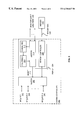
- FIG. 1 shows a block diagram of a computer system in accordance with one embodiment of the invention.
- FIG. 2 shows an expanded block diagram of a memory interface circuit in accordance with FIG. 1 .
- FIG. 3 shows an expanded block diagram of the configuration register and counters of FIG. 2 .
- FIG. 4 shows a flowchart of memory interface processing in accordance with one embodiment of the invention.
- Each device/process capable of requesting system memory access (hereinafter referred to as a requestor) may be assigned an access count value.
- a requestor's access count value determines the number of consecutive memory access cycles it may use before a different device is allowed to access memory.
- FIG. 1 shows a block diagram of computer system 100 incorporating system controller 102 and memory interface 104 in accordance with one embodiment of the invention.
- system controller 102 couples processor 106 , accelerated graphics port (AGP) device 108 , system bus 110 and devices connected thereto (e.g., devices 112 and secondary bus bridge circuit 114 ) to system memory 116 (via memory bus 118 ).
- AGP accelerated graphics port
- secondary bus bridge circuit 114 provides a mechanism to couple secondary bus 120 and attached devices to system memory 116 .
- non-volatile memory 122 and other secondary bus devices (e.g., device 124 ) such as floppy disks may be coupled directly to secondary bus 122 while one or more intelligent drive electronics (IDE) devices may be coupled to system 100 via IDE interface 126 , and one or more universal serial bus (USB) devices may be coupled to system 100 via USB interface 128 .
- IDE intelligent drive electronics
- USB universal serial bus
- memory interface 104 determines an access count value for each requester that may access system memory 116 . In another embodiment, memory interface 104 determines an access count value for each type of requestor that may access system memory 116 . For example, all processors (e.g., processor 106 ) may be assigned a common access count value as may all AGP devices (e.g., device 108 ). In yet another embodiment, some devices (e.g., a specific processor or a specific primary bus device) may have specifically assigned access count values while other devices may have assigned access count values based on their type.
- processors e.g., processor 106
- AGP devices e.g., device 108
- some devices e.g., a specific processor or a specific primary bus device
- a requestor may access system memory 116 up to N consecutive times (where N equals the requestor's assigned access count value) before another requestor is granted access.
- requesters may be assigned access count values commensurate with their natural memory transaction size. For example, requests initiated by processor 106 are typically for a cache line's worth of data (e.g., 256 bits or 32 bytes). Thus, a processor requestor may be assigned a access count value sufficient to transfer 32 bytes of data between itself and system memory. Thus, if system memory 116 is accessed via 64-bit (32-bit) words, a processor requestor may be assigned an access count value of 4 (8).
- block devices such as graphics devices (e.g., AGP device 108 and one or more system bus devices 112 ) may naturally initiate memory transactions of 8 kilobytes (KB). These devices may be assigned access count values sufficient to transfer 8 KB.
- illustrative processors include the PENTIUM® processor and 80 ⁇ 86 families of processors from Intel Corporation.
- An illustrative system bus (e.g., bus 110 ) is one operated in conformance with the Peripheral Component Interconnect (PCI) specification.
- Illustrative primary bus devices 112 include audio, network interface, video and graphics accelerator PCI expansion card devices.
- An illustrative secondary bus bridge circuit (e.g., bridge circuit 114 ) is the PIIX4 PCI-to-ISA/IDE accelerator chip from Intel Corporation.
- Illustrative secondary buses include those bus structures operated in conformance with the Low Pin Count (LPC) interface, Industry Standard Architecture (ISA) and Extended Industry Standard Architecture (EISA) standards.
- Illustrative non-volatile memory devices e.g., NVRAM 126
- ROM read only memory
- EPROM electrically programmable read only memory
- EEPROM electrically erasable programmable read only memory
- flash memory and complementary metal oxide semiconductor (CMOS) memory.
- CMOS complementary metal oxide semiconductor
- Illustrative secondary bus devices e.g., device 128
- input-output device controllers e.g., audio and modem devices. It will be recognized that each of the elements of FIG. 1 are typically connected, directly or indirectly, to a printed circuit board often referred to as a motherboard. It will be further recognized that motherboards often include embedded devices (a digital signal processor, for example) that may communicate with system memory 116 via system controller 102 .
- FIG. 2 shows system controller 102 and an expanded block diagram of memory interface 104 in accordance with one embodiment of the invention.
- switch 200 may be used to route memory request signals 202 through 206 between requesting devices and memory interface 104 .
- Each request signal represents a signal path between system controller 102 and a requesting device (e.g., processor 108 and secondary bus device 124 ).
- a requesting device e.g., processor 108 and secondary bus device 124
- memory request signals e.g., 202
- memory request signals typically encode information identifying the device issuing the memory request, the amount of memory being requested (to read or write), a memory transaction address, and other information as needed by other system controller functions.
- Memory interface 104 includes memory controller 208 , arbiter 210 , configuration register 212 , and one or more counters 214 .
- Memory controller 208 processes selected memory access request signals, transferring data into and out of memory 116 in accordance with conventional memory controller operations.
- Arbiter 210 determines which request signal (via select signal 216 ) is routed by switch 200 to memory controller 208 for processing.
- arbiter 210 implements a grant-request handshake protocol wherein each device that may access memory 116 has a corresponding grant/request signal pair 218 .
- arbiter 210 monitors grant/request signals 218 and, in combination with configuration registers 214 and counters 216 selectively passes one request signal at a time between switch 200 and memory controller 208 .
- Configuration registers 212 may be used to record access count values for each requestor (or class of requester), and counters 214 may be used by arbiter 210 to track the number of memory access operations remaining for a selected requestor.
- configuration register 212 may have a plurality of fields, each field adapted to store an access count value for a single requestor.
- field-1 300 may record an access count value for processor 106
- field-2 302 may record an access count value for AGP device 108
- field-N 304 may store an access count value for secondary bus device 124 .
- Counters e.g., 306 , 308 and 310
- arbiter 210 are used by arbiter 210 to track the number of memory access operations that remain allocated to a selected requestor. Each access by a requestor causes its associated counter value to be decremented.
- arbiter 210 When the counter reaches 0 (zero), or the requester deasserts its request signal (on grant/request signal pairs 218 ), arbiter 210 performs an arbitration cycle—selecting a different requestor or the same requestor (depending upon the arbitration scheme).
- the number of counters may equal the number of access count value fields in configuration register 212 .
- counter 214 may comprise a single counter which is loaded with the appropriate configuration field value when a device is initially selected, decremented each access thereafter, and reloaded when another device is selected by arbiter 210 .
- Arbiter 210 initially chooses one device from the plurality of devices that may access memory 116 (block 400 ). Arbiter 210 may, for example, implement a round-robin arbitration mechanism in which requestors are chosen during block 400 in a predetermined and cyclic pattern. If the chosen device does not have a pending memory request (the ‘no’ prong of diamond 402 ), the next requestor is chosen and processing continues at block 400 .
- arbiter 210 selects the chosen device by loading the access count value associated with the selected device from configuration register 212 to counter 214 , and causing switch 200 to couple the selected requestor (request signal 204 , for example) to memory 116 via memory controller 208 (block 404 ).
- Memory controller 208 performs a single memory access operation in accordance with the selected memory request (block 406 ), the requestor's associated counter value is decremented (block 408 ), and a check is made to determine if the selected device has completed all of its allocated consecutive accesses (diamond 410 ).
- processing continues at block 406 . If the selected device's counter value is zero, or the selected device deasserts it memory request signal (the ‘yes’ prong of diamond 410 ), processing continues at block 406 . If the selected associated device's counter value greater than zero (the ‘no’ prong of diamond 410 ), processing continues at block 406 .
- configuration register 212 is initialized during computer system power on self-test (POST) operations by basic input-output system (BIOS) routines 130 (see FIG. 1 ).
- POST computer system power on self-test
- BIOS basic input-output system
- configuration register 212 may reside in PCI configuration address space.
- requester access count values may be determined dynamically at computer system start up and/or modified during system operations. For example, access count values may be based on requestor operating speed, wherein faster devices are allocated larger access count values.
- system controller 102 or memory interface 104 may monitor (snoop) memory bus 118 activity and empirically set and adjust requestor access count values (i.e., modify values stored in configuration register 212 )—wherein the more frequently a requester seeks to access memory 116 (relative to other requesters), the larger its access count value is set.
- requestor access count values i.e., modify values stored in configuration register 212
- FIGS. 1 and 2 show memory interface 104 as being one element within system controller 102 .
- a memory interface in accordance with the invention may be implemented as a stand-alone circuit. That is, memory interface 104 may be implemented as one or more custom designed state machines, embodied in a hardware device such as a printed circuit board comprising discrete logic, integrated circuits, or specially designed application specific integrated circuits (ASICs).
- ASICs application specific integrated circuits
- a requestor may have different access count values for read and write memory transactions. That is, configuration register 212 may provide two fields per requestor—one field adapted to store a read operation access count value and another field adapted to store a write operation access count value.
Abstract
Description
Claims (19)
Priority Applications (1)
| Application Number | Priority Date | Filing Date | Title |
|---|---|---|---|
| US09/386,973 US6330647B1 (en) | 1999-08-31 | 1999-08-31 | Memory bandwidth allocation based on access count priority scheme |
Applications Claiming Priority (1)
| Application Number | Priority Date | Filing Date | Title |
|---|---|---|---|
| US09/386,973 US6330647B1 (en) | 1999-08-31 | 1999-08-31 | Memory bandwidth allocation based on access count priority scheme |
Publications (1)
| Publication Number | Publication Date |
|---|---|
| US6330647B1 true US6330647B1 (en) | 2001-12-11 |
Family
ID=23527873
Family Applications (1)
| Application Number | Title | Priority Date | Filing Date |
|---|---|---|---|
| US09/386,973 Expired - Lifetime US6330647B1 (en) | 1999-08-31 | 1999-08-31 | Memory bandwidth allocation based on access count priority scheme |
Country Status (1)
| Country | Link |
|---|---|
| US (1) | US6330647B1 (en) |
Cited By (52)
| Publication number | Priority date | Publication date | Assignee | Title |
|---|---|---|---|---|
| US6654837B1 (en) * | 1999-12-28 | 2003-11-25 | Intel Corporation | Dynamic priority external transaction system |
| US20040059879A1 (en) * | 2002-09-23 | 2004-03-25 | Rogers Paul L. | Access priority protocol for computer system |
| US20040088467A1 (en) * | 2002-10-31 | 2004-05-06 | Burton Lee A. | System and method for providing an arbitrated memory bus in a hybrid computing system |
| US20050223150A1 (en) * | 2004-03-31 | 2005-10-06 | Masao Ohmoto | Resource management device, resource management system, and resource management method |
| US20050283634A1 (en) * | 2004-06-22 | 2005-12-22 | Rai Barinder S | Method and apparatus for adaptively adjusting the bandwidth of a data transmission channel having multiple buffered paths |
| US7062582B1 (en) * | 2003-03-14 | 2006-06-13 | Marvell International Ltd. | Method and apparatus for bus arbitration dynamic priority based on waiting period |
| US20060248624A1 (en) * | 2005-04-25 | 2006-11-09 | Pieczynski Darren E | Heat containment hand warming device |
| US7149857B2 (en) | 2002-05-14 | 2006-12-12 | Micron Technology, Inc. | Out of order DRAM sequencer |
| US7155722B1 (en) * | 2001-07-10 | 2006-12-26 | Cisco Technology, Inc. | System and method for process load balancing in a multi-processor environment |
| GB2437322A (en) * | 2006-04-17 | 2007-10-24 | Realtek Semiconductor Corp | System and method for bandwidth sharing in buses |
| US20080091866A1 (en) * | 2006-10-12 | 2008-04-17 | International Business Machines Corporation | Maintaining forward progress in a shared L2 by detecting and breaking up requestor starvation |
| US20080195825A1 (en) * | 2007-02-08 | 2008-08-14 | Analog Devices, Inc. | Metrics modules and methods for monitoring, analyzing and optimizing bus and memory operations in a complex integrated circuit |
| US20080215782A1 (en) * | 2004-06-24 | 2008-09-04 | Tetsuji Mochida | Administration Device For Warranting Local Concentrated Access in Low-Band Width, Administration Method, and Animation Processing Apparatus Including the Administration Device |
| US20080242152A1 (en) * | 2007-03-30 | 2008-10-02 | Hon Hai Precision Industry Co., Ltd. | Pci express interface card |
| US20080263249A1 (en) * | 2005-01-31 | 2008-10-23 | Matsushita Electric Industrial Co., Ltd. | Access Arbiter and Arbitrable Condition Verification Device |
| US20090070774A1 (en) * | 2007-09-12 | 2009-03-12 | Shlomo Raikin | Live lock free priority scheme for memory transactions in transactional memory |
| US7538772B1 (en) * | 2000-08-23 | 2009-05-26 | Nintendo Co., Ltd. | Graphics processing system with enhanced memory controller |
| WO2010011220A1 (en) * | 2008-07-23 | 2010-01-28 | Micro Motion, Inc. | Processing system with external memory access control |
| US20100023653A1 (en) * | 2008-07-25 | 2010-01-28 | Anton Rozen | System and method for arbitrating between memory access requests |
| US20110055443A1 (en) * | 2008-05-13 | 2011-03-03 | Panasonic Corporation | Memory control apparatus and information processing apparatus including the same |
| US20110258186A1 (en) * | 2006-07-28 | 2011-10-20 | Diskeeper Corporation | Assigning data for storage based on a frequency with which the data is accessed |
| US20110320643A1 (en) * | 2010-06-23 | 2011-12-29 | International Business Machines Corporation | Measurement facility for adapter functions |
| US20130054856A1 (en) * | 2011-08-31 | 2013-02-28 | Kie Woon Lim | Providing Adaptive Bandwidth Allocation For A Fixed Priority Arbiter |
| US8458387B2 (en) | 2010-06-23 | 2013-06-04 | International Business Machines Corporation | Converting a message signaled interruption into an I/O adapter event notification to a guest operating system |
| US8505032B2 (en) | 2010-06-23 | 2013-08-06 | International Business Machines Corporation | Operating system notification of actions to be taken responsive to adapter events |
| US8510599B2 (en) | 2010-06-23 | 2013-08-13 | International Business Machines Corporation | Managing processing associated with hardware events |
| US8549182B2 (en) | 2010-06-23 | 2013-10-01 | International Business Machines Corporation | Store/store block instructions for communicating with adapters |
| US8566480B2 (en) | 2010-06-23 | 2013-10-22 | International Business Machines Corporation | Load instruction for communicating with adapters |
| US8601497B2 (en) | 2010-06-23 | 2013-12-03 | International Business Machines Corporation | Converting a message signaled interruption into an I/O adapter event notification |
| US8615645B2 (en) | 2010-06-23 | 2013-12-24 | International Business Machines Corporation | Controlling the selectively setting of operational parameters for an adapter |
| US8621112B2 (en) | 2010-06-23 | 2013-12-31 | International Business Machines Corporation | Discovery by operating system of information relating to adapter functions accessible to the operating system |
| US8626970B2 (en) | 2010-06-23 | 2014-01-07 | International Business Machines Corporation | Controlling access by a configuration to an adapter function |
| US8631222B2 (en) | 2010-06-23 | 2014-01-14 | International Business Machines Corporation | Translation of input/output addresses to memory addresses |
| US8639858B2 (en) | 2010-06-23 | 2014-01-28 | International Business Machines Corporation | Resizing address spaces concurrent to accessing the address spaces |
| US8650337B2 (en) | 2010-06-23 | 2014-02-11 | International Business Machines Corporation | Runtime determination of translation formats for adapter functions |
| US9021156B2 (en) | 2011-08-31 | 2015-04-28 | Prashanth Nimmala | Integrating intellectual property (IP) blocks into a processor |
| US9053251B2 (en) | 2011-11-29 | 2015-06-09 | Intel Corporation | Providing a sideband message interface for system on a chip (SoC) |
| US9064051B2 (en) | 2011-09-29 | 2015-06-23 | Intel Corporation | Issuing requests to a fabric |
| US9122815B2 (en) | 2011-09-29 | 2015-09-01 | Intel Corporation | Common idle state, active state and credit management for an interface |
| US9195623B2 (en) | 2010-06-23 | 2015-11-24 | International Business Machines Corporation | Multiple address spaces per adapter with address translation |
| US9213661B2 (en) | 2010-06-23 | 2015-12-15 | International Business Machines Corporation | Enable/disable adapters of a computing environment |
| US9270576B2 (en) | 2011-09-29 | 2016-02-23 | Intel Corporation | Aggregating completion messages in a sideband interface |
| US9342352B2 (en) | 2010-06-23 | 2016-05-17 | International Business Machines Corporation | Guest access to address spaces of adapter |
| US9448870B2 (en) | 2011-09-29 | 2016-09-20 | Intel Corporation | Providing error handling support to legacy devices |
| US9489329B2 (en) | 2011-09-29 | 2016-11-08 | Intel Corporation | Supporting multiple channels of a single interface |
| US9658978B2 (en) | 2011-09-29 | 2017-05-23 | Intel Corporation | Providing multiple decode options for a system-on-chip (SoC) fabric |
| US10164880B2 (en) | 2011-09-29 | 2018-12-25 | Intel Corporation | Sending packets with expanded headers |
| US10846126B2 (en) | 2016-12-28 | 2020-11-24 | Intel Corporation | Method, apparatus and system for handling non-posted memory write transactions in a fabric |
| US10911261B2 (en) | 2016-12-19 | 2021-02-02 | Intel Corporation | Method, apparatus and system for hierarchical network on chip routing |
| US11232031B2 (en) * | 2016-11-23 | 2022-01-25 | Huawei Technologies Co., Ltd. | Allocation of memory ranks based on access traffic |
| US11561918B1 (en) * | 2020-05-15 | 2023-01-24 | Amazon Technologies, Inc. | Communication bus recovery based on maximum allowable transaction duration |
| US20230393783A1 (en) * | 2022-06-02 | 2023-12-07 | Micron Technology, Inc. | Access heatmap generation at a memory device |
Citations (11)
| Publication number | Priority date | Publication date | Assignee | Title |
|---|---|---|---|---|
| US5212795A (en) * | 1988-10-11 | 1993-05-18 | California Institute Of Technology | Programmable DMA controller |
| US5241644A (en) * | 1987-07-15 | 1993-08-31 | Nec Corporation | Queue having long word length |
| US5666516A (en) * | 1993-12-16 | 1997-09-09 | International Business Machines Corporation | Protected programmable memory cartridge having selective access circuitry |
| US5727150A (en) * | 1995-05-05 | 1998-03-10 | Silicon Graphics, Inc. | Apparatus and method for page migration in a non-uniform memory access (NUMA) system |
| US5960468A (en) * | 1997-04-30 | 1999-09-28 | Sony Corporation | Asynchronous memory interface for a video processor with a 2N sized buffer and N+1 bit wide gray coded counters |
| US5987574A (en) * | 1997-04-30 | 1999-11-16 | Sony Corporation | Bank arbitration for SDRAM memory control |
| US6006303A (en) * | 1997-08-28 | 1999-12-21 | Oki Electric Industry Co., Inc. | Priority encoding and decoding for memory architecture |
| US6024472A (en) * | 1997-08-06 | 2000-02-15 | Tseng; Chian-Yin | Automobile with angle-adjustable front lamp device for providing an angle of irradiation that varies in accordance with rotation of a steering wheel |
| US6032232A (en) * | 1997-05-29 | 2000-02-29 | 3Com Corporation | Multiported memory access system with arbitration and a source burst limiter for blocking a memory access request |
| US6035378A (en) * | 1997-12-16 | 2000-03-07 | Ncr Corporation | Method and apparatus for dynamically monitoring memory page access frequency in a non-uniform memory access computer system |
| US6035377A (en) * | 1997-12-17 | 2000-03-07 | Ncr Corporation | Method and apparatus for determining memory pages having greatest frequency of access in a non-uniform memory access computer system |
-
1999
- 1999-08-31 US US09/386,973 patent/US6330647B1/en not_active Expired - Lifetime
Patent Citations (12)
| Publication number | Priority date | Publication date | Assignee | Title |
|---|---|---|---|---|
| US5241644A (en) * | 1987-07-15 | 1993-08-31 | Nec Corporation | Queue having long word length |
| US5212795A (en) * | 1988-10-11 | 1993-05-18 | California Institute Of Technology | Programmable DMA controller |
| US5666516A (en) * | 1993-12-16 | 1997-09-09 | International Business Machines Corporation | Protected programmable memory cartridge having selective access circuitry |
| US5765197A (en) * | 1993-12-16 | 1998-06-09 | International Business Machines Corporation | Method and system for authentication of a memory unit for a computer system |
| US5727150A (en) * | 1995-05-05 | 1998-03-10 | Silicon Graphics, Inc. | Apparatus and method for page migration in a non-uniform memory access (NUMA) system |
| US5960468A (en) * | 1997-04-30 | 1999-09-28 | Sony Corporation | Asynchronous memory interface for a video processor with a 2N sized buffer and N+1 bit wide gray coded counters |
| US5987574A (en) * | 1997-04-30 | 1999-11-16 | Sony Corporation | Bank arbitration for SDRAM memory control |
| US6032232A (en) * | 1997-05-29 | 2000-02-29 | 3Com Corporation | Multiported memory access system with arbitration and a source burst limiter for blocking a memory access request |
| US6024472A (en) * | 1997-08-06 | 2000-02-15 | Tseng; Chian-Yin | Automobile with angle-adjustable front lamp device for providing an angle of irradiation that varies in accordance with rotation of a steering wheel |
| US6006303A (en) * | 1997-08-28 | 1999-12-21 | Oki Electric Industry Co., Inc. | Priority encoding and decoding for memory architecture |
| US6035378A (en) * | 1997-12-16 | 2000-03-07 | Ncr Corporation | Method and apparatus for dynamically monitoring memory page access frequency in a non-uniform memory access computer system |
| US6035377A (en) * | 1997-12-17 | 2000-03-07 | Ncr Corporation | Method and apparatus for determining memory pages having greatest frequency of access in a non-uniform memory access computer system |
Cited By (92)
| Publication number | Priority date | Publication date | Assignee | Title |
|---|---|---|---|---|
| US7143242B2 (en) * | 1999-12-28 | 2006-11-28 | Intel Corporation | Dynamic priority external transaction system |
| US6654837B1 (en) * | 1999-12-28 | 2003-11-25 | Intel Corporation | Dynamic priority external transaction system |
| US20040059854A1 (en) * | 1999-12-28 | 2004-03-25 | Hill David L. | Dynamic priority external transaction system |
| US8098255B2 (en) * | 2000-08-23 | 2012-01-17 | Nintendo Co., Ltd. | Graphics processing system with enhanced memory controller |
| US7538772B1 (en) * | 2000-08-23 | 2009-05-26 | Nintendo Co., Ltd. | Graphics processing system with enhanced memory controller |
| US7155722B1 (en) * | 2001-07-10 | 2006-12-26 | Cisco Technology, Inc. | System and method for process load balancing in a multi-processor environment |
| US7620789B2 (en) | 2002-05-14 | 2009-11-17 | Micron Technology, Inc. | Out of order DRAM sequencer |
| US9904489B2 (en) | 2002-05-14 | 2018-02-27 | Micron Technology, Inc. | Processing systems, memory controllers and methods for controlling memory access operations |
| US7149857B2 (en) | 2002-05-14 | 2006-12-12 | Micron Technology, Inc. | Out of order DRAM sequencer |
| US20070101075A1 (en) * | 2002-05-14 | 2007-05-03 | Jeddeloh Joseph M | Out of order DRAM sequencer |
| US8639902B2 (en) | 2002-05-14 | 2014-01-28 | Micron Technology, Inc. | Methods for sequencing memory access requests |
| US20040059879A1 (en) * | 2002-09-23 | 2004-03-25 | Rogers Paul L. | Access priority protocol for computer system |
| FR2845177A1 (en) * | 2002-09-23 | 2004-04-02 | Hewlett Packard Development Co | ACCESS PRIORITY PROTOCOL FOR COMPUTER SYSTEM |
| US20040088467A1 (en) * | 2002-10-31 | 2004-05-06 | Burton Lee A. | System and method for providing an arbitrated memory bus in a hybrid computing system |
| US6996656B2 (en) * | 2002-10-31 | 2006-02-07 | Src Computers, Inc. | System and method for providing an arbitrated memory bus in a hybrid computing system |
| WO2004042588A1 (en) * | 2002-10-31 | 2004-05-21 | Src Computers, Inc. | System and method for providing an arbitrated memory bus in a hybrid computing system |
| US7698486B1 (en) | 2003-03-14 | 2010-04-13 | Marvell International Ltd. | Method and apparatus for bus arbitration dynamic priority based on waiting period |
| US9037767B1 (en) | 2003-03-14 | 2015-05-19 | Marvell International Ltd. | Method and apparatus for dynamically granting access of a shared resource among a plurality of requestors |
| US7062582B1 (en) * | 2003-03-14 | 2006-06-13 | Marvell International Ltd. | Method and apparatus for bus arbitration dynamic priority based on waiting period |
| US8041870B1 (en) | 2003-03-14 | 2011-10-18 | Marvell International Ltd. | Method and apparatus for dynamically granting access of a shared resource among a plurality of requestors |
| US8307139B1 (en) | 2003-03-14 | 2012-11-06 | Marvell International Ltd. | Method and apparatus for dynamically granting access of a shared resource among a plurality of requestors |
| US20050223150A1 (en) * | 2004-03-31 | 2005-10-06 | Masao Ohmoto | Resource management device, resource management system, and resource management method |
| US20050283634A1 (en) * | 2004-06-22 | 2005-12-22 | Rai Barinder S | Method and apparatus for adaptively adjusting the bandwidth of a data transmission channel having multiple buffered paths |
| US7366816B2 (en) | 2004-06-22 | 2008-04-29 | Seiko Epson Corporation | Method and apparatus for adaptively adjusting the bandwidth of a data transmission channel having multiple buffered paths |
| US20100005209A1 (en) * | 2004-06-24 | 2010-01-07 | Tetsuji Mochida | Arbitration device for arbitrating among a plurality of master devices, arbitration method, and video processing device including the arbitration device |
| US7725633B2 (en) * | 2004-06-24 | 2010-05-25 | Panasonic Corporation | Arbitration device for arbitrating among a plurality of master devices, arbitration method, and video processing device including the arbitration device |
| US7779190B2 (en) | 2004-06-24 | 2010-08-17 | Panasonic Corporation | Arbitration device for arbitrating among a plurality of master devices, arbitration method, and video processing device including the arbitration device |
| US20080215782A1 (en) * | 2004-06-24 | 2008-09-04 | Tetsuji Mochida | Administration Device For Warranting Local Concentrated Access in Low-Band Width, Administration Method, and Animation Processing Apparatus Including the Administration Device |
| US20080263249A1 (en) * | 2005-01-31 | 2008-10-23 | Matsushita Electric Industrial Co., Ltd. | Access Arbiter and Arbitrable Condition Verification Device |
| US7739437B2 (en) * | 2005-01-31 | 2010-06-15 | Panasonic Corporation | Access arbiter and arbitrable condition verification device |
| US20060248624A1 (en) * | 2005-04-25 | 2006-11-09 | Pieczynski Darren E | Heat containment hand warming device |
| GB2437322A (en) * | 2006-04-17 | 2007-10-24 | Realtek Semiconductor Corp | System and method for bandwidth sharing in buses |
| GB2437322B (en) * | 2006-04-17 | 2008-11-26 | Realtek Semiconductor Corp | System and method for bandwidth sharing in busses |
| US8732148B2 (en) * | 2006-07-28 | 2014-05-20 | Condusiv Technologies Corporation | Assigning data for storage based on a frequency with which the data is accessed |
| US20110258186A1 (en) * | 2006-07-28 | 2011-10-20 | Diskeeper Corporation | Assigning data for storage based on a frequency with which the data is accessed |
| US20080091866A1 (en) * | 2006-10-12 | 2008-04-17 | International Business Machines Corporation | Maintaining forward progress in a shared L2 by detecting and breaking up requestor starvation |
| US20080195825A1 (en) * | 2007-02-08 | 2008-08-14 | Analog Devices, Inc. | Metrics modules and methods for monitoring, analyzing and optimizing bus and memory operations in a complex integrated circuit |
| US7702862B2 (en) * | 2007-02-08 | 2010-04-20 | Analog Devices, Inc. | Metrics modules and methods for monitoring, analyzing and optimizing bus and memory operations in a complex integrated circuit |
| US20080242152A1 (en) * | 2007-03-30 | 2008-10-02 | Hon Hai Precision Industry Co., Ltd. | Pci express interface card |
| US8209689B2 (en) * | 2007-09-12 | 2012-06-26 | Intel Corporation | Live lock free priority scheme for memory transactions in transactional memory |
| US20090070774A1 (en) * | 2007-09-12 | 2009-03-12 | Shlomo Raikin | Live lock free priority scheme for memory transactions in transactional memory |
| US20110055443A1 (en) * | 2008-05-13 | 2011-03-03 | Panasonic Corporation | Memory control apparatus and information processing apparatus including the same |
| CN102105870A (en) * | 2008-07-23 | 2011-06-22 | 微动公司 | Processing system with external memory access control |
| AU2008359713B2 (en) * | 2008-07-23 | 2012-12-13 | Micro Motion, Inc. | Processing system with external memory access control |
| RU2568306C1 (en) * | 2008-07-23 | 2015-11-20 | Майкро Моушн, Инк. | Processing system with external memory access control |
| CN102105870B (en) * | 2008-07-23 | 2015-05-20 | 微动公司 | Processing system with external memory access control |
| WO2010011220A1 (en) * | 2008-07-23 | 2010-01-28 | Micro Motion, Inc. | Processing system with external memory access control |
| US20110113173A1 (en) * | 2008-07-23 | 2011-05-12 | Hays Paul J | Processing system with external memory access control |
| US8688943B2 (en) | 2008-07-23 | 2014-04-01 | Micro Motion, Inc. | Processing system with external memory access control |
| US8171187B2 (en) * | 2008-07-25 | 2012-05-01 | Freescale Semiconductor, Inc. | System and method for arbitrating between memory access requests |
| US20100023653A1 (en) * | 2008-07-25 | 2010-01-28 | Anton Rozen | System and method for arbitrating between memory access requests |
| US8505032B2 (en) | 2010-06-23 | 2013-08-06 | International Business Machines Corporation | Operating system notification of actions to be taken responsive to adapter events |
| US8549182B2 (en) | 2010-06-23 | 2013-10-01 | International Business Machines Corporation | Store/store block instructions for communicating with adapters |
| US8621112B2 (en) | 2010-06-23 | 2013-12-31 | International Business Machines Corporation | Discovery by operating system of information relating to adapter functions accessible to the operating system |
| US8626970B2 (en) | 2010-06-23 | 2014-01-07 | International Business Machines Corporation | Controlling access by a configuration to an adapter function |
| US8631222B2 (en) | 2010-06-23 | 2014-01-14 | International Business Machines Corporation | Translation of input/output addresses to memory addresses |
| US8635430B2 (en) | 2010-06-23 | 2014-01-21 | International Business Machines Corporation | Translation of input/output addresses to memory addresses |
| US8601497B2 (en) | 2010-06-23 | 2013-12-03 | International Business Machines Corporation | Converting a message signaled interruption into an I/O adapter event notification |
| US8639858B2 (en) | 2010-06-23 | 2014-01-28 | International Business Machines Corporation | Resizing address spaces concurrent to accessing the address spaces |
| US8650337B2 (en) | 2010-06-23 | 2014-02-11 | International Business Machines Corporation | Runtime determination of translation formats for adapter functions |
| US8650335B2 (en) * | 2010-06-23 | 2014-02-11 | International Business Machines Corporation | Measurement facility for adapter functions |
| US8566480B2 (en) | 2010-06-23 | 2013-10-22 | International Business Machines Corporation | Load instruction for communicating with adapters |
| US8615645B2 (en) | 2010-06-23 | 2013-12-24 | International Business Machines Corporation | Controlling the selectively setting of operational parameters for an adapter |
| US20110320643A1 (en) * | 2010-06-23 | 2011-12-29 | International Business Machines Corporation | Measurement facility for adapter functions |
| US9626298B2 (en) | 2010-06-23 | 2017-04-18 | International Business Machines Corporation | Translation of input/output addresses to memory addresses |
| US8510599B2 (en) | 2010-06-23 | 2013-08-13 | International Business Machines Corporation | Managing processing associated with hardware events |
| US8458387B2 (en) | 2010-06-23 | 2013-06-04 | International Business Machines Corporation | Converting a message signaled interruption into an I/O adapter event notification to a guest operating system |
| US9383931B2 (en) | 2010-06-23 | 2016-07-05 | International Business Machines Corporation | Controlling the selectively setting of operational parameters for an adapter |
| US9342352B2 (en) | 2010-06-23 | 2016-05-17 | International Business Machines Corporation | Guest access to address spaces of adapter |
| US9213661B2 (en) | 2010-06-23 | 2015-12-15 | International Business Machines Corporation | Enable/disable adapters of a computing environment |
| US9195623B2 (en) | 2010-06-23 | 2015-11-24 | International Business Machines Corporation | Multiple address spaces per adapter with address translation |
| US9134911B2 (en) | 2010-06-23 | 2015-09-15 | International Business Machines Corporation | Store peripheral component interconnect (PCI) function controls instruction |
| US20130054856A1 (en) * | 2011-08-31 | 2013-02-28 | Kie Woon Lim | Providing Adaptive Bandwidth Allocation For A Fixed Priority Arbiter |
| US9021156B2 (en) | 2011-08-31 | 2015-04-28 | Prashanth Nimmala | Integrating intellectual property (IP) blocks into a processor |
| US8930602B2 (en) * | 2011-08-31 | 2015-01-06 | Intel Corporation | Providing adaptive bandwidth allocation for a fixed priority arbiter |
| US9064051B2 (en) | 2011-09-29 | 2015-06-23 | Intel Corporation | Issuing requests to a fabric |
| US9270576B2 (en) | 2011-09-29 | 2016-02-23 | Intel Corporation | Aggregating completion messages in a sideband interface |
| US9122815B2 (en) | 2011-09-29 | 2015-09-01 | Intel Corporation | Common idle state, active state and credit management for an interface |
| US10164880B2 (en) | 2011-09-29 | 2018-12-25 | Intel Corporation | Sending packets with expanded headers |
| US9448870B2 (en) | 2011-09-29 | 2016-09-20 | Intel Corporation | Providing error handling support to legacy devices |
| US9489329B2 (en) | 2011-09-29 | 2016-11-08 | Intel Corporation | Supporting multiple channels of a single interface |
| US9075929B2 (en) | 2011-09-29 | 2015-07-07 | Intel Corporation | Issuing requests to a fabric |
| US9658978B2 (en) | 2011-09-29 | 2017-05-23 | Intel Corporation | Providing multiple decode options for a system-on-chip (SoC) fabric |
| US9753875B2 (en) | 2011-09-29 | 2017-09-05 | Intel Corporation | Systems and an apparatus with a sideband interface interconnecting agents with at least one router |
| US9213666B2 (en) | 2011-11-29 | 2015-12-15 | Intel Corporation | Providing a sideband message interface for system on a chip (SoC) |
| US9053251B2 (en) | 2011-11-29 | 2015-06-09 | Intel Corporation | Providing a sideband message interface for system on a chip (SoC) |
| US11232031B2 (en) * | 2016-11-23 | 2022-01-25 | Huawei Technologies Co., Ltd. | Allocation of memory ranks based on access traffic |
| US10911261B2 (en) | 2016-12-19 | 2021-02-02 | Intel Corporation | Method, apparatus and system for hierarchical network on chip routing |
| US10846126B2 (en) | 2016-12-28 | 2020-11-24 | Intel Corporation | Method, apparatus and system for handling non-posted memory write transactions in a fabric |
| US11372674B2 (en) | 2016-12-28 | 2022-06-28 | Intel Corporation | Method, apparatus and system for handling non-posted memory write transactions in a fabric |
| US11561918B1 (en) * | 2020-05-15 | 2023-01-24 | Amazon Technologies, Inc. | Communication bus recovery based on maximum allowable transaction duration |
| US20230393783A1 (en) * | 2022-06-02 | 2023-12-07 | Micron Technology, Inc. | Access heatmap generation at a memory device |
Similar Documents
| Publication | Publication Date | Title |
|---|---|---|
| US6330647B1 (en) | Memory bandwidth allocation based on access count priority scheme | |
| KR100420706B1 (en) | Method and system for I / O control in multiprocessor system using simultaneous access of variable width bus | |
| KR100420707B1 (en) | Method and system for bus arbitration in multiprocessor systems with simultaneous access of variable-width buses | |
| US6775727B2 (en) | System and method for controlling bus arbitration during cache memory burst cycles | |
| US6006303A (en) | Priority encoding and decoding for memory architecture | |
| US7003593B2 (en) | Computer system architecture and memory controller for close-coupling within a hybrid processing system utilizing an adaptive processor interface port | |
| US6662251B2 (en) | Selective targeting of transactions to devices on a shared bus | |
| US6704821B2 (en) | Arbitration method and circuit architecture therefore | |
| KR100296718B1 (en) | Method and system for simultaneously accessing variable-width buses in multiprocessor systems | |
| EP1163593B1 (en) | Apparatus for communicating between multiple functional units in a computer environment | |
| US20050256994A1 (en) | System and method for providing an arbitrated memory bus in a hybrid computing system | |
| US6012116A (en) | Apparatus and method for controlling data, address, and enable buses within a microprocessor | |
| US5828891A (en) | Multilevel interrupt device | |
| US6604159B1 (en) | Data release to reduce latency in on-chip system bus | |
| US6615295B2 (en) | Relaxed read completion ordering in a system using transaction order queue | |
| US7080174B1 (en) | System and method for managing input/output requests using a fairness throttle | |
| US5933613A (en) | Computer system and inter-bus control circuit | |
| US6889283B2 (en) | Method and system to promote arbitration priority in a buffer queue | |
| US7028116B2 (en) | Enhancement of transaction order queue | |
| US6016526A (en) | Method and apparatus for transferring data between buses having differing ordering policies via the use of autonomous units | |
| JP2004062910A (en) | Method for realizing semaphore to multi-core processor and controlling access to common resource | |
| US6775758B2 (en) | Buffer page roll implementation for PCI-X block read transactions | |
| US5951668A (en) | Method and system for transferring data between buses having differing ordering policies | |
| US6003102A (en) | Apparatus and method for arbitrating transactions requiring multiple addresses | |
| US5901299A (en) | Method and apparatus for transferring data between buses having differing ordering policies |
Legal Events
| Date | Code | Title | Description |
|---|---|---|---|
| AS | Assignment |
Owner name: MICRON ELECTRONICS, INC., IDAHO Free format text: ASSIGNMENT OF ASSIGNORS INTEREST;ASSIGNORS:JEDDELOH, JOSEPH M.;LARSON, DOUGLAS A.;REEL/FRAME:010214/0151 Effective date: 19990824 |
|
| AS | Assignment |
Owner name: MICRON TECHNOLOGY, INC., IOWA Free format text: ASSIGNMENT OF ASSIGNORS INTEREST;ASSIGNOR:MICRON ELECTRONICS, INC.;REEL/FRAME:010763/0572 Effective date: 20000317 |
|
| STCF | Information on status: patent grant |
Free format text: PATENTED CASE |
|
| FPAY | Fee payment |
Year of fee payment: 4 |
|
| FPAY | Fee payment |
Year of fee payment: 8 |
|
| FPAY | Fee payment |
Year of fee payment: 12 |
|
| AS | Assignment |
Owner name: U.S. BANK NATIONAL ASSOCIATION, AS COLLATERAL AGENT, CALIFORNIA Free format text: SECURITY INTEREST;ASSIGNOR:MICRON TECHNOLOGY, INC.;REEL/FRAME:038669/0001 Effective date: 20160426 Owner name: U.S. BANK NATIONAL ASSOCIATION, AS COLLATERAL AGEN Free format text: SECURITY INTEREST;ASSIGNOR:MICRON TECHNOLOGY, INC.;REEL/FRAME:038669/0001 Effective date: 20160426 |
|
| AS | Assignment |
Owner name: MORGAN STANLEY SENIOR FUNDING, INC., AS COLLATERAL AGENT, MARYLAND Free format text: PATENT SECURITY AGREEMENT;ASSIGNOR:MICRON TECHNOLOGY, INC.;REEL/FRAME:038954/0001 Effective date: 20160426 Owner name: MORGAN STANLEY SENIOR FUNDING, INC., AS COLLATERAL Free format text: PATENT SECURITY AGREEMENT;ASSIGNOR:MICRON TECHNOLOGY, INC.;REEL/FRAME:038954/0001 Effective date: 20160426 |
|
| AS | Assignment |
Owner name: U.S. BANK NATIONAL ASSOCIATION, AS COLLATERAL AGENT, CALIFORNIA Free format text: CORRECTIVE ASSIGNMENT TO CORRECT THE REPLACE ERRONEOUSLY FILED PATENT #7358718 WITH THE CORRECT PATENT #7358178 PREVIOUSLY RECORDED ON REEL 038669 FRAME 0001. ASSIGNOR(S) HEREBY CONFIRMS THE SECURITY INTEREST;ASSIGNOR:MICRON TECHNOLOGY, INC.;REEL/FRAME:043079/0001 Effective date: 20160426 Owner name: U.S. BANK NATIONAL ASSOCIATION, AS COLLATERAL AGEN Free format text: CORRECTIVE ASSIGNMENT TO CORRECT THE REPLACE ERRONEOUSLY FILED PATENT #7358718 WITH THE CORRECT PATENT #7358178 PREVIOUSLY RECORDED ON REEL 038669 FRAME 0001. ASSIGNOR(S) HEREBY CONFIRMS THE SECURITY INTEREST;ASSIGNOR:MICRON TECHNOLOGY, INC.;REEL/FRAME:043079/0001 Effective date: 20160426 |
|
| AS | Assignment |
Owner name: JPMORGAN CHASE BANK, N.A., AS COLLATERAL AGENT, ILLINOIS Free format text: SECURITY INTEREST;ASSIGNORS:MICRON TECHNOLOGY, INC.;MICRON SEMICONDUCTOR PRODUCTS, INC.;REEL/FRAME:047540/0001 Effective date: 20180703 Owner name: JPMORGAN CHASE BANK, N.A., AS COLLATERAL AGENT, IL Free format text: SECURITY INTEREST;ASSIGNORS:MICRON TECHNOLOGY, INC.;MICRON SEMICONDUCTOR PRODUCTS, INC.;REEL/FRAME:047540/0001 Effective date: 20180703 |
|
| AS | Assignment |
Owner name: MICRON TECHNOLOGY, INC., IDAHO Free format text: RELEASE BY SECURED PARTY;ASSIGNOR:U.S. BANK NATIONAL ASSOCIATION, AS COLLATERAL AGENT;REEL/FRAME:047243/0001 Effective date: 20180629 |
|
| AS | Assignment |
Owner name: MICRON TECHNOLOGY, INC., IDAHO Free format text: RELEASE BY SECURED PARTY;ASSIGNOR:MORGAN STANLEY SENIOR FUNDING, INC., AS COLLATERAL AGENT;REEL/FRAME:050937/0001 Effective date: 20190731 |
|
| AS | Assignment |
Owner name: MICRON TECHNOLOGY, INC., IDAHO Free format text: RELEASE BY SECURED PARTY;ASSIGNOR:JPMORGAN CHASE BANK, N.A., AS COLLATERAL AGENT;REEL/FRAME:051028/0001 Effective date: 20190731 Owner name: MICRON SEMICONDUCTOR PRODUCTS, INC., IDAHO Free format text: RELEASE BY SECURED PARTY;ASSIGNOR:JPMORGAN CHASE BANK, N.A., AS COLLATERAL AGENT;REEL/FRAME:051028/0001 Effective date: 20190731 |