US6323045B1 - Method and structure for top-to-bottom I/O nets repair in a thin film transfer and join process - Google Patents

Method and structure for top-to-bottom I/O nets repair in a thin film transfer and join process Download PDF

Info

Publication number
US6323045B1
US6323045B1 US09/456,590 US45659099A US6323045B1 US 6323045 B1 US6323045 B1 US 6323045B1 US 45659099 A US45659099 A US 45659099A US 6323045 B1 US6323045 B1 US 6323045B1
Authority
US
United States
Prior art keywords
thin film
repair
net
location
defective
Prior art date
Legal status (The legal status is an assumption and is not a legal conclusion. Google has not performed a legal analysis and makes no representation as to the accuracy of the status listed.)
Expired - Fee Related
Application number
US09/456,590
Inventor
Christopher Cline
Nancy W. Hannon
Chandrika Prasad
Thomas A. Wassick
Roy Yu
Current Assignee (The listed assignees may be inaccurate. Google has not performed a legal analysis and makes no representation or warranty as to the accuracy of the list.)
International Business Machines Corp
Original Assignee
International Business Machines Corp
Priority date (The priority date is an assumption and is not a legal conclusion. Google has not performed a legal analysis and makes no representation as to the accuracy of the date listed.)
Filing date
Publication date
Application filed by International Business Machines Corp filed Critical International Business Machines Corp
Priority to US09/456,590 priority Critical patent/US6323045B1/en
Assigned to INTERNATIONAL BUSINESS MACHINES CORPORATION reassignment INTERNATIONAL BUSINESS MACHINES CORPORATION ASSIGNMENT OF ASSIGNORS INTEREST (SEE DOCUMENT FOR DETAILS). Assignors: PRASAD, CHANDRIKA, WASSICK, THOMAS A., HANNON, NANCY W., CLINE, CHRISTOPHER, YU, ROY
Application granted granted Critical
Publication of US6323045B1 publication Critical patent/US6323045B1/en
Anticipated expiration legal-status Critical
Expired - Fee Related legal-status Critical Current

Links

Images

Classifications

    • HELECTRICITY
    • H05ELECTRIC TECHNIQUES NOT OTHERWISE PROVIDED FOR
    • H05KPRINTED CIRCUITS; CASINGS OR CONSTRUCTIONAL DETAILS OF ELECTRIC APPARATUS; MANUFACTURE OF ASSEMBLAGES OF ELECTRICAL COMPONENTS
    • H05K3/00Apparatus or processes for manufacturing printed circuits
    • H05K3/22Secondary treatment of printed circuits
    • H05K3/225Correcting or repairing of printed circuits
    • HELECTRICITY
    • H01ELECTRIC ELEMENTS
    • H01LSEMICONDUCTOR DEVICES NOT COVERED BY CLASS H10
    • H01L21/00Processes or apparatus adapted for the manufacture or treatment of semiconductor or solid state devices or of parts thereof
    • H01L21/02Manufacture or treatment of semiconductor devices or of parts thereof
    • H01L21/04Manufacture or treatment of semiconductor devices or of parts thereof the devices having at least one potential-jump barrier or surface barrier, e.g. PN junction, depletion layer or carrier concentration layer
    • H01L21/48Manufacture or treatment of parts, e.g. containers, prior to assembly of the devices, using processes not provided for in a single one of the subgroups H01L21/06 - H01L21/326
    • H01L21/4814Conductive parts
    • H01L21/4846Leads on or in insulating or insulated substrates, e.g. metallisation
    • H01L21/485Adaptation of interconnections, e.g. engineering charges, repair techniques
    • HELECTRICITY
    • H01ELECTRIC ELEMENTS
    • H01LSEMICONDUCTOR DEVICES NOT COVERED BY CLASS H10
    • H01L23/00Details of semiconductor or other solid state devices
    • H01L23/52Arrangements for conducting electric current within the device in operation from one component to another, i.e. interconnections, e.g. wires, lead frames
    • H01L23/538Arrangements for conducting electric current within the device in operation from one component to another, i.e. interconnections, e.g. wires, lead frames the interconnection structure between a plurality of semiconductor chips being formed on, or in, insulating substrates
    • H01L23/5382Adaptable interconnections, e.g. for engineering changes
    • HELECTRICITY
    • H01ELECTRIC ELEMENTS
    • H01LSEMICONDUCTOR DEVICES NOT COVERED BY CLASS H10
    • H01L2924/00Indexing scheme for arrangements or methods for connecting or disconnecting semiconductor or solid-state bodies as covered by H01L24/00
    • H01L2924/0001Technical content checked by a classifier
    • H01L2924/0002Not covered by any one of groups H01L24/00, H01L24/00 and H01L2224/00

Definitions

  • the present invention generally relates to repair of defective wiring connections in thin film multi-chip modules or chip carriers, and, more particularly, to the repair of thin film wiring using embedded metallurgy (TSM) repair schemes.
  • TSM embedded metallurgy
  • TSM Topic Surface Metal
  • FIG. 1 illustrates a portion of a conventional multi-chip module (MCM) before repair.
  • C 4 connection 10 is connected to net 12 at via 14 .
  • X repair line 16 and Y repair lines 18 , 20 are part of the top layer.
  • Y repair lines 18 , 20 are connected by Y repair line subway 22 using vias 24 , 26 .
  • Vias 14 , 25 , 26 connect to down levels.
  • C 4 connection 10 has a repair elbow 28 and a bond site 30 .
  • FIG. 2 is a plan view of the portion of the device shown in FIG. 1 after the conventional repair process.
  • FIG. 3 is a cross-sectional view taken along the line 3 — 3 of FIG. 2.
  • top-to-top wiring nets which connect chip C 4 through the thin film layers structure
  • top-to-bottom nets which connect C 4 to peripheral I/O
  • all I/O repairs are made on a case by case basis, and partial repair and sacrificial repair methods have been employed for some special and simple I/O defects situations.
  • a direct I/O plate-up repair method is a general repair approach, however, the current TF designs do not contain the needed repair features connecting capture pads (C/P) to C 4 pads.
  • the I/O repairability is also a slow and elaborate task, and does not have the manufacturability required for a production line.
  • a multilayer thin film module is typically processed on the surface of a MLC (Multi-Level Ceramic) carrier.
  • MLC Multi-Level Ceramic
  • a full after-thin-film test is performed to confirm the integrity of the thin film structure.
  • a defect is found to be associated with a top-to-bottom I/O net, then the part is in general considered unrepairable and will be rejected.
  • the present invention is directed to a device repair process that uses unused capture pads for top-to-bottom I/O repair. Since there are a substantial number of C 4 and C/P that are not normally used, they can be paired up to form connections from the capture pads at the bottom of the thin film, to the C 4 's at the top of the thin films. In this way, the C/P-C 4 pairing forms z-repair lines in the thin film structure by forming alternative passages from the capture pad to the C 4 .
  • TFTJ thin film transfer-joining
  • This z-repair line concept is the foundation for I/O repairability of TF in a TFTJ process. If an I/O net is found defective in the thin film wiring prior to joining to the ceramic carrier, the corresponding capture pad on the ceramic top surface is rewired to a nearby z-repair line site. The connection from the substrate to the capture pad of the defective I/O net is disconnected by means of via blocking or solder ball removal. Since the z-repair line will give the I/O an alternative path to the thin film top surface, a repair of a defective I/O net can be made.
  • the original defective thin film portion of the I/O net is disconnected on the top surface from the C 4 by standard laser delete and then wired to the TSM z-repair feature using conventional repair methodologies. In this way, the I/O net can be repaired via the z-repair lines embedded in the TF structure as part of the design.
  • the solder joining between the ceramic and thin film on the repaired I/O site is preferably removed to eliminate the antenna effect on the remaining TF net.
  • the key features of this invention are the creation of alternative wiring paths between C 4 's and the bottom surface of the thin film portion of the structure (spare vertical connections), the creation of a simple wiring pattern of X and Y lines on the surface of the ceramic substrate to which the thin film transfer will be mated, and a method to remove or block the solder ball connection from the defective net during joining of the thin film to the ceramic using the solder lamination process.
  • FIG. 1 is a plan view of a portion of a prior art multi-chip module (MCM) before repair.
  • MCM multi-chip module
  • FIG. 2 is a plan view of the portion of the device shown in FIG. 1 after the conventional repair process.
  • FIG. 3 is a cross-sectional view taken along the line 3 — 3 of FIG. 2 .
  • FIG. 4 is an illustration of a TFTJ on ceramic, where FIG. 4 ( a ) is a cross-sectional view showing the I/O net and a z-repair line according to the invention, FIG. 4 ( b ) is a top view of the C/P joining surface of the ceramic, FIG. 4 ( c ) is a cross-sectional blow-up of a capture pad, and FIG. 4 ( d ) is a cross-sectional blow-up of a via.
  • the thin film structure 40 is built with the top surface metallurgy 42 up on a glass carrier (not shown), as shown in FIG. 4 ( a ).
  • the structure 40 is flipped over to a secondary glass carrier (not shown) to expose the bottom surface 48 (I/O) of the TF structure 40 .
  • This step is at the preparation step prior to joining the TF to a ceramic carrier 46 .
  • both top and bottom surfaces 48 , 50 of TF are now accessible due to this flip-flop approach, repair of the I/O nets is possible in this TSM up TFTJ process.
  • the repair methodology proceeds as follows for a defective net 52 . (This repair process is preferably repeated for each defective net 52 .)
  • a defective I/O net 52 is identified for repair using conventional test or inspection techniques, with both the C 4 54 and the solder joining pad 56 and mating pad 60 locations of the net 52 already established. Any constraints associated with the I/O net 52 are understood, e.g. minimum and maximum lengths, net topography, etc.
  • a spare C 4 / capture pad z-repair path 58 is chosen from those available in the design. They are chosen based on the wiring rules established to insure electrical functionality and equivalence. This can be optimized by relying on graphically assisted wiring tools or through an automated routing system generally known in the art.
  • the defective portion 64 of the I/O net 52 is then disconnected at the C 4 54 by cutting of the delete strap on the top surface (not shown).
  • the C 4 54 is wired to the spare z-repair 58 chosen in the previous step by way of C 4 100 , again insuring compliance with the wiring rules.
  • This rewiring is done using conventional repair methodologies (e.g., spot expose, LSR shunt add, etc.).
  • the spare capture pad 102 is wired to the capture pad 60 of the defective net 52 using the repair paths available, again insuring compliance with the wiring rules. This is done using conventional repair methodologies, as described above.
  • the solder connection 66 from the defective net 52 capture pad 60 is then eliminated.
  • the ceramic 46 and thin film 44 are joined standard, completing the repair, and the structure is tested to insure electrical functionality.
  • FIG. 4 illustrates the completed TFTJ structure after repair. (Note: The chip to chip C 4 connections are not shown in this representation).
  • FIG. 4 ( b ) is a top plan view of the surface 70 of the ceramic 46 to which the thin film transfer body 44 is joined. It is on this surface 70 that the alternative wiring path structures 104 are placed to permit the rerouting of defective I/O nets 52 . Also shown are the connections 72 from defective 1 /O net 52 (FIG. 4 ( a )) to the spare capture pad 102 of the z-repair line 58 (FIG. 4 ( a )) in the C/P plane.
  • the dark circles 76 shown in FIG. 4 ( b ) represent the capture pads 60 , and preferably comprise nickel-gold BLM (Ball Limiting Metallurgy) with solder.
  • the larger circles 54 preferably are Cr/Cu/Cr and represent capture pads 60 that are used to buffer stress to the ceramic 46 as well as to provide lands for repair bonds.
  • the invention provides for the creation of alternative wiring paths between C 4 's 54 and the bottom surface 48 of the thin film portion 42 of the structure 40 (spare vertical connections). Since the presence of alternative wiring can create congestion that could impact the wiring of the module, these spare features are better designed after the initial wiring of the thin film 42 is complete. In this way, clear areas, spare C 4 's 100 and spare capture pads 102 can be easily identified and connected. Numerous connections can be established according to this technique, especially in I/O intensive areas, to permit multiple wiring paths.
  • the creation of a simple wiring pattern of X and Y lines on the surface of the ceramic substrate 46 is also provided to which the thin film transfer 42 will be mated. This consists of lines 104 with areas that would facilitate joining of discrete bonds to make new connections. These areas are functionally similar to the structures used on the top surface 50 of the thin films 42 for standard net repair. It is also feasible to alternatively have these wiring patterns on the underside 48 of the thin film transfer 42 instead of on the ceramic 46 surface.
  • the ceramic 46 side wiring could be in one level or in multiple levels, depending on the requirements of the substrate.
  • the preferred structure is to have the repair paths on the ceramic 46 —this simplifies the processing and gives improved cycle times by keeping more of the processing in parallel.
  • a method is also provided to remove or block the solder ball connection 66 from the defective net 52 during the joining of the thin film 42 to the ceramic 46 using a solder lamination process. This is preferably achieved by removal of the ball 66 , elimination of the via 78 (see FIG. 4 ( c )) between the underside 48 of the thin film 42 and the solder pad 56 on the thin film side, elimination of the via 82 (see FIG. 4 ( d )) between the ceramic 46 and the solder joining 76 on the ceramic side, or other such methods generally known in the art.

Abstract

A method and structure for providing top-to-bottom repair of a defective I/O net in a thin film transfer and join process. At least one C4 location and at least one capture pad are provided on a thin film substrate. The substrate is preferably ceramic. The C4 location of the defective net is severed by removal of a delete strap. The corresponding solder connection of the associated capture pad is also removed. A spare C4 location and capture pad are connected to provide a Z-repair line imbedded in the TF wiring structure. The Z-repair line is wired to the defective net.

Description

FIELD OF THE INVENTION
The present invention generally relates to repair of defective wiring connections in thin film multi-chip modules or chip carriers, and, more particularly, to the repair of thin film wiring using embedded metallurgy (TSM) repair schemes.
BACKGROUND OF THE INVENTION
The repair of thin film wiring using TSM (Top Surface Metal) repair lines is well known. In the conventional repair process, a defective electrical wiring net, used to connect components on a multichip carrier, is disconnected from its internal wiring through specialized delete locations located at the “C4” (Controlled-Collapsed-Chip-Connection) joining, pads. The net is reconstructed with equivalent electrical performance by connecting the X-Y grid of the repair lines on the top surface to the required C4 pads, matching the timing of the original net.
The reconstruction of the net is normally accomplished by joining the segments of the surface repair lines with individual gold ribbons bonded to the TSM repair lines through a lasersonic bonding methodology. The gold ribbons interconnect specific X and Y repair line segments to rebuild the net topography. FIG. 1 illustrates a portion of a conventional multi-chip module (MCM) before repair. In FIG. 1, C4 connection 10 is connected to net 12 at via 14. X repair line 16 and Y repair lines 18, 20 are part of the top layer. Y repair lines 18, 20 are connected by Y repair line subway 22 using vias 24, 26. Vias 14, 25, 26 connect to down levels. C4 connection 10 has a repair elbow 28 and a bond site 30.
FIG. 2 is a plan view of the portion of the device shown in FIG. 1 after the conventional repair process. (FIG. 3 is a cross-sectional view taken along the line 33 of FIG. 2.) When a defect is found in net 12, it is completely disconnected from the circuit using external delete 32 between C4 connection 10 and via 14. This process is repeated at every other C4 connection location for net 12. To replace this deleted net, a portion of X repair line 16 and Y repair lines 18, 20 must be used. Conventionally, X repair line 16 and Y repair lines 18, 20 are cut using deletes. Then, C4 connection 10 is connected to X repair line 16 using gold ribbon 34, and X repair line 16 is connected to Y repair line 20 using gold ribbon 36.
In a multi-layer thin film structure, most of the top-to-top wiring nets, which connect chip C4 through the thin film layers structure, can be repaired via top surface repair lines. For top-to-bottom nets, which connect C4 to peripheral I/O, however, there is no established repair methodology. Presently, all I/O repairs are made on a case by case basis, and partial repair and sacrificial repair methods have been employed for some special and simple I/O defects situations. A direct I/O plate-up repair method is a general repair approach, however, the current TF designs do not contain the needed repair features connecting capture pads (C/P) to C4 pads. The I/O repairability is also a slow and elaborate task, and does not have the manufacturability required for a production line.
A multilayer thin film module is typically processed on the surface of a MLC (Multi-Level Ceramic) carrier. After the structure is built, a full after-thin-film test is performed to confirm the integrity of the thin film structure. At this stage, if a defect is found to be associated with a top-to-bottom I/O net, then the part is in general considered unrepairable and will be rejected. There are some special situations when an I/O defect can be repaired by employing the concept and technique of graphical assisted partial repair. In general, however, there is no systematically established method to repair top-to-bottom I/O nets. The reason for the unrepairability in I/O nets is simply the inaccessibility of the top-to-bottom portion of I/O nets in the thin film on ceramic carrier design structure.
In a typical TF wiring design, about 30% of the capture pads (C/P) and 50% of the C4 (chip joining sites) are not used. Currently, these unused pads are only filled in by design and have no functionality.
In view of the shortcomings of the prior art, a reliable TF processing alternative is needed to improve the top-to-bottom repair process of thin film products.
SUMMARY OF THE INVENTION
To meet this and other needs, the present invention is directed to a device repair process that uses unused capture pads for top-to-bottom I/O repair. Since there are a substantial number of C4 and C/P that are not normally used, they can be paired up to form connections from the capture pads at the bottom of the thin film, to the C4's at the top of the thin films. In this way, the C/P-C4 pairing forms z-repair lines in the thin film structure by forming alternative passages from the capture pad to the C4.
Of the many unique features of thin film transfer-joining (TFTJ) technology, one of them is top-to-bottom I/O repairability. This z-repair line concept is the foundation for I/O repairability of TF in a TFTJ process. If an I/O net is found defective in the thin film wiring prior to joining to the ceramic carrier, the corresponding capture pad on the ceramic top surface is rewired to a nearby z-repair line site. The connection from the substrate to the capture pad of the defective I/O net is disconnected by means of via blocking or solder ball removal. Since the z-repair line will give the I/O an alternative path to the thin film top surface, a repair of a defective I/O net can be made. The original defective thin film portion of the I/O net is disconnected on the top surface from the C4 by standard laser delete and then wired to the TSM z-repair feature using conventional repair methodologies. In this way, the I/O net can be repaired via the z-repair lines embedded in the TF structure as part of the design. The solder joining between the ceramic and thin film on the repaired I/O site is preferably removed to eliminate the antenna effect on the remaining TF net.
The key features of this invention are the creation of alternative wiring paths between C4's and the bottom surface of the thin film portion of the structure (spare vertical connections), the creation of a simple wiring pattern of X and Y lines on the surface of the ceramic substrate to which the thin film transfer will be mated, and a method to remove or block the solder ball connection from the defective net during joining of the thin film to the ceramic using the solder lamination process.
These and other features and advantages of the invention will become apparent to those skilled in the art upon a review of the following detailed description of the presently preferred embodiments of the invention, viewed in conjunction with the appended drawings.
BRIEF DESCRIPTION OF THE DRAWINGS
FIG. 1 is a plan view of a portion of a prior art multi-chip module (MCM) before repair.
FIG. 2 is a plan view of the portion of the device shown in FIG. 1 after the conventional repair process.
FIG. 3 is a cross-sectional view taken along the line 33 of FIG. 2.
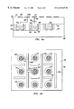
FIG. 4 is an illustration of a TFTJ on ceramic, where FIG. 4(a) is a cross-sectional view showing the I/O net and a z-repair line according to the invention, FIG. 4(b) is a top view of the C/P joining surface of the ceramic, FIG. 4(c) is a cross-sectional blow-up of a capture pad, and FIG. 4(d) is a cross-sectional blow-up of a via.
DETAILED DESCRIPTION OF THE PRESENTLY PREFERRED EMBODIMENTS OF THE INVENTION
Referring now to the drawings, where like elements receive like reference numerals throughout, in the proposed TFTJ process, the thin film structure 40 is built with the top surface metallurgy 42 up on a glass carrier (not shown), as shown in FIG. 4(a). After test and repair, the structure 40 is flipped over to a secondary glass carrier (not shown) to expose the bottom surface 48 (I/O) of the TF structure 40. This step is at the preparation step prior to joining the TF to a ceramic carrier 46. However, since both top and bottom surfaces 48, 50 of TF are now accessible due to this flip-flop approach, repair of the I/O nets is possible in this TSM up TFTJ process.
The repair methodology proceeds as follows for a defective net 52. (This repair process is preferably repeated for each defective net 52.) A defective I/O net 52 is identified for repair using conventional test or inspection techniques, with both the C4 54 and the solder joining pad 56 and mating pad 60 locations of the net 52 already established. Any constraints associated with the I/O net 52 are understood, e.g. minimum and maximum lengths, net topography, etc. A spare C4 / capture pad z-repair path 58 is chosen from those available in the design. They are chosen based on the wiring rules established to insure electrical functionality and equivalence. This can be optimized by relying on graphically assisted wiring tools or through an automated routing system generally known in the art.
The defective portion 64 of the I/O net 52 is then disconnected at the C4 54 by cutting of the delete strap on the top surface (not shown). The C4 54 is wired to the spare z-repair 58 chosen in the previous step by way of C4 100, again insuring compliance with the wiring rules. This rewiring is done using conventional repair methodologies (e.g., spot expose, LSR shunt add, etc.). The spare capture pad 102 is wired to the capture pad 60 of the defective net 52 using the repair paths available, again insuring compliance with the wiring rules. This is done using conventional repair methodologies, as described above. The solder connection 66 from the defective net 52 capture pad 60 is then eliminated. The ceramic 46 and thin film 44 are joined standard, completing the repair, and the structure is tested to insure electrical functionality. FIG. 4 illustrates the completed TFTJ structure after repair. (Note: The chip to chip C4 connections are not shown in this representation).
FIG. 4(b) is a top plan view of the surface 70 of the ceramic 46 to which the thin film transfer body 44 is joined. It is on this surface 70 that the alternative wiring path structures 104 are placed to permit the rerouting of defective I/O nets 52. Also shown are the connections 72 from defective 1/O net 52 (FIG. 4(a)) to the spare capture pad 102 of the z-repair line 58 (FIG. 4(a)) in the C/P plane. The dark circles 76 shown in FIG. 4(b) represent the capture pads 60, and preferably comprise nickel-gold BLM (Ball Limiting Metallurgy) with solder. The larger circles 54 preferably are Cr/Cu/Cr and represent capture pads 60 that are used to buffer stress to the ceramic 46 as well as to provide lands for repair bonds.
As can be seen, the invention provides for the creation of alternative wiring paths between C4's 54 and the bottom surface 48 of the thin film portion 42 of the structure 40 (spare vertical connections). Since the presence of alternative wiring can create congestion that could impact the wiring of the module, these spare features are better designed after the initial wiring of the thin film 42 is complete. In this way, clear areas, spare C4's 100 and spare capture pads 102 can be easily identified and connected. Numerous connections can be established according to this technique, especially in I/O intensive areas, to permit multiple wiring paths.
The creation of a simple wiring pattern of X and Y lines on the surface of the ceramic substrate 46 is also provided to which the thin film transfer 42 will be mated. This consists of lines 104 with areas that would facilitate joining of discrete bonds to make new connections. These areas are functionally similar to the structures used on the top surface 50 of the thin films 42 for standard net repair. It is also feasible to alternatively have these wiring patterns on the underside 48 of the thin film transfer 42 instead of on the ceramic 46 surface. The ceramic 46 side wiring could be in one level or in multiple levels, depending on the requirements of the substrate. The preferred structure is to have the repair paths on the ceramic 46—this simplifies the processing and gives improved cycle times by keeping more of the processing in parallel.
A method is also provided to remove or block the solder ball connection 66 from the defective net 52 during the joining of the thin film 42 to the ceramic 46 using a solder lamination process. This is preferably achieved by removal of the ball 66, elimination of the via 78 (see FIG. 4(c)) between the underside 48 of the thin film 42 and the solder pad 56 on the thin film side, elimination of the via 82 (see FIG. 4(d)) between the ceramic 46 and the solder joining 76 on the ceramic side, or other such methods generally known in the art.
It is to be understood that a wide range of changes and modifications to the embodiments described above will be apparent to those skilled in the art and are contemplated. It is therefore intended that the foregoing detailed description be regarded as illustrative, rather than limiting, and that it be understood that it is the following claims, including all equivalents, that are intended to define the spirit and scope of the invention.

Claims (16)

What is claimed is:
1. A method for top-to-bottom I/O net repair in a thin film transfer and join process, comprising the steps of:
providing a C4 location and a capture pad on a thin film CHIP CARRIER;
identifying a defective net on the thin film WIRING and the associated C4 location;
disconnecting the C4 location associated with the defective net;
identifying a spare C4 location and corresponding capture pad to provide a z-repair line in the thin film; and
rewiring the defective net to the z-repair line to match the functionality of a non-defective net.
2. The method defined in claim 1, further comprising the step of identifying the defective net through conventional test or inspection techniques.
3. The method defined in claim 1, further comprising the step of providing a plurality of C4 locations and capture pads.
4. The method defined in claim 1, further comprising the step of disconnecting the defective net at the C4 location by cutting a delete strap.
5. The method defined in claim 1, wherein the rewiring step comprises conventional repair methodologies.
6. The method defined in claim 1, further comprising the step of eliminating a solder connection between the defective net and the associated capture pad.
7. The method defined in claim 6, wherein the step of eliminating the solder connection comprises removal of a solder ball.
8. The method defined in claim 6, wherein the step of eliminating the solder connection comprises elimination of a via connecting a solder pad to a substrate or thin film.
9. The method defined in claim 6, wherein the step of eliminating the solder connection comprises blocking of a solder pad with insulating material to prevent solder joining.
10. A top-to-bottom I/O net repair structure in a thin film transfer and join process, comprising:
a thin film transfer disposed on a ceramic substrate;
a C4 location and a capture pad disposed on the thin film ceramic substrate;
a defective net having an associated C4 location and capture pad;
a spare C4 location and corresponding capture pad coupled to provide a z-repair line in the thin film ceramic substrate;
an open circuit connection between the defective net and the associated C4 location; and
a connection between the capture pad of the defective net and that of the spare Z repair line.
11. The structure defined in claim 10, wherein the capture pad comprises a chromium copper composite.
12. The structure defined in claim 10, wherein the solder joining surfaces comprises nickel or nickel-gold composites.
13. The structure defined in claim 10, wherein the C4 location comprises plural C4 locations.
14. The structure defined in claim 10, wherein the capture pad comprises plural capture pads.
15. The structure defined in claim 10, further comprising a delete strap coupled to the defective net.
16. The structure defined in claim 10, further comprising a solderless connection between the defective net and the associated capture pad.
US09/456,590 1999-12-08 1999-12-08 Method and structure for top-to-bottom I/O nets repair in a thin film transfer and join process Expired - Fee Related US6323045B1 (en)

Priority Applications (1)

Application Number Priority Date Filing Date Title
US09/456,590 US6323045B1 (en) 1999-12-08 1999-12-08 Method and structure for top-to-bottom I/O nets repair in a thin film transfer and join process

Applications Claiming Priority (1)

Application Number Priority Date Filing Date Title
US09/456,590 US6323045B1 (en) 1999-12-08 1999-12-08 Method and structure for top-to-bottom I/O nets repair in a thin film transfer and join process

Publications (1)

Publication Number Publication Date
US6323045B1 true US6323045B1 (en) 2001-11-27

Family

ID=23813378

Family Applications (1)

Application Number Title Priority Date Filing Date
US09/456,590 Expired - Fee Related US6323045B1 (en) 1999-12-08 1999-12-08 Method and structure for top-to-bottom I/O nets repair in a thin film transfer and join process

Country Status (1)

Country Link
US (1) US6323045B1 (en)

Cited By (5)

* Cited by examiner, † Cited by third party
Publication number Priority date Publication date Assignee Title
US8035213B2 (en) 2007-10-22 2011-10-11 Advanced Semiconductor Engineering, Inc. Chip package structure and method of manufacturing the same
US8884424B2 (en) 2010-01-13 2014-11-11 Advanced Semiconductor Engineering, Inc. Semiconductor package with single sided substrate design and manufacturing methods thereof
US20150131249A1 (en) * 2013-11-12 2015-05-14 Infineon Technologies Ag Solder Bridging Prevention Structures for Circuit Boards and Semiconductor Packages
US9349611B2 (en) 2010-03-22 2016-05-24 Advanced Semiconductor Engineering, Inc. Stackable semiconductor package and manufacturing method thereof
US9406658B2 (en) 2010-12-17 2016-08-02 Advanced Semiconductor Engineering, Inc. Embedded component device and manufacturing methods thereof

Citations (11)

* Cited by examiner, † Cited by third party
Publication number Priority date Publication date Assignee Title
US4304450A (en) 1979-12-17 1981-12-08 International Business Machines Corporation Repair of open circuited gas discharge display panel conductors
US4453176A (en) 1981-12-31 1984-06-05 International Business Machines Corporation LSI Chip carrier with buried repairable capacitor with low inductance leads
US4817850A (en) 1988-03-28 1989-04-04 Hughes Aircraft Company Repairable flip-chip bumping
US4894708A (en) 1983-07-19 1990-01-16 Nec Corporation LSI package having a multilayer ceramic substrate
US5299160A (en) 1992-06-02 1994-03-29 Mitsubishi Denki Kabushiki Kaisha Semiconductor memory device capable of repairing defective bits
US5493076A (en) 1993-10-15 1996-02-20 International Business Machines Corporation Structure for repairing semiconductor substrates
US5532853A (en) 1993-03-04 1996-07-02 Samsung Electronics Co., Ltd. Reparable display device matrix for repairing the electrical connection of a bonding pad to its associated signal line
US5725995A (en) 1988-05-16 1998-03-10 Elm Technology Corporation Method of repairing defective traces in an integrated circuit structure
US5841193A (en) 1996-05-20 1998-11-24 Epic Technologies, Inc. Single chip modules, repairable multichip modules, and methods of fabrication thereof
US5895230A (en) * 1996-01-31 1999-04-20 International Business Machines Corporation Integrated circuit chip package having configurable contacts and method for making the same
US6159657A (en) * 1999-08-31 2000-12-12 Eastman Kodak Company Thermal imaging composition and member containing sulfonated ir dye and methods of imaging and printing

Patent Citations (11)

* Cited by examiner, † Cited by third party
Publication number Priority date Publication date Assignee Title
US4304450A (en) 1979-12-17 1981-12-08 International Business Machines Corporation Repair of open circuited gas discharge display panel conductors
US4453176A (en) 1981-12-31 1984-06-05 International Business Machines Corporation LSI Chip carrier with buried repairable capacitor with low inductance leads
US4894708A (en) 1983-07-19 1990-01-16 Nec Corporation LSI package having a multilayer ceramic substrate
US4817850A (en) 1988-03-28 1989-04-04 Hughes Aircraft Company Repairable flip-chip bumping
US5725995A (en) 1988-05-16 1998-03-10 Elm Technology Corporation Method of repairing defective traces in an integrated circuit structure
US5299160A (en) 1992-06-02 1994-03-29 Mitsubishi Denki Kabushiki Kaisha Semiconductor memory device capable of repairing defective bits
US5532853A (en) 1993-03-04 1996-07-02 Samsung Electronics Co., Ltd. Reparable display device matrix for repairing the electrical connection of a bonding pad to its associated signal line
US5493076A (en) 1993-10-15 1996-02-20 International Business Machines Corporation Structure for repairing semiconductor substrates
US5895230A (en) * 1996-01-31 1999-04-20 International Business Machines Corporation Integrated circuit chip package having configurable contacts and method for making the same
US5841193A (en) 1996-05-20 1998-11-24 Epic Technologies, Inc. Single chip modules, repairable multichip modules, and methods of fabrication thereof
US6159657A (en) * 1999-08-31 2000-12-12 Eastman Kodak Company Thermal imaging composition and member containing sulfonated ir dye and methods of imaging and printing

Cited By (10)

* Cited by examiner, † Cited by third party
Publication number Priority date Publication date Assignee Title
US8035213B2 (en) 2007-10-22 2011-10-11 Advanced Semiconductor Engineering, Inc. Chip package structure and method of manufacturing the same
US8884424B2 (en) 2010-01-13 2014-11-11 Advanced Semiconductor Engineering, Inc. Semiconductor package with single sided substrate design and manufacturing methods thereof
US9196597B2 (en) 2010-01-13 2015-11-24 Advanced Semiconductor Engineering, Inc. Semiconductor package with single sided substrate design and manufacturing methods thereof
US9349611B2 (en) 2010-03-22 2016-05-24 Advanced Semiconductor Engineering, Inc. Stackable semiconductor package and manufacturing method thereof
US9406658B2 (en) 2010-12-17 2016-08-02 Advanced Semiconductor Engineering, Inc. Embedded component device and manufacturing methods thereof
US20150131249A1 (en) * 2013-11-12 2015-05-14 Infineon Technologies Ag Solder Bridging Prevention Structures for Circuit Boards and Semiconductor Packages
CN104637906A (en) * 2013-11-12 2015-05-20 英飞凌科技股份有限公司 Solder bridging prevention structures for circuit boards and semiconductor packages
CN104637906B (en) * 2013-11-12 2017-10-13 英飞凌科技股份有限公司 Structure is prevented for circuit substrate and the solder of semiconductor packages bridge joint
US10085353B2 (en) * 2013-11-12 2018-09-25 Infineon Technologies Ag Solder bridging prevention structures for circuit boards and semiconductor packages
DE102014116522B4 (en) 2013-11-12 2021-10-14 Infineon Technologies Ag Structures to protect against solder bridges in printed circuit boards, semiconductor packages and semiconductor assemblies

Similar Documents

Publication Publication Date Title
US4817850A (en) Repairable flip-chip bumping
US8404977B2 (en) Flexible circuit assembly without solder
EP0178227B1 (en) Integrated circuit semiconductor device formed on a wafer
KR100278093B1 (en) Method of Mounting Resilient Contact Structures to Semiconductor Devices
US6861284B2 (en) Semiconductor device and production method thereof
KR0168463B1 (en) Debondable metallic bonding method
US3739232A (en) Interconnected electrical circuit board assembly and method of fabrication
US20060008944A1 (en) Substrate having built-in semiconductor apparatus and manufacturing method thereof
EP0083405A2 (en) Chip carrier for large scale integrated circuits and a method for the fabrication of the carrier
JP2007059931A (en) Method for fitting spring element onto semiconductor device and for testing wafer level
KR20010031602A (en) Semiconductor device and method for manufacturing the same
JPH05218288A (en) Multilayer thin-film module
US7342248B2 (en) Semiconductor device and interposer
US6427324B1 (en) Inherently robust repair process for thin film circuitry using UV laser
US6323045B1 (en) Method and structure for top-to-bottom I/O nets repair in a thin film transfer and join process
US20020039807A1 (en) Manufacturing method of a semiconductor device
JP2001326250A (en) Flip-chip semiconductor device and method of manufacture
JPH0823015A (en) Preparation of known-good die with solder bump
JP2001284520A (en) Circuit board for semiconductor chip mounting, manufacturing method for the circuit board, circuit board for relay connecting, semiconductor device and connecting structure between the semiconductor devices
CN1228827C (en) Semiconductor chip package and process of operation
CN105655321A (en) Electronic packages and methods of making and using same
Tosaya et al. Router flip chip packaging solution and reliability
US7015132B2 (en) Forming an electrical contact on an electronic component
US20040000709A1 (en) Internal package interconnect with electrically parallel vias
KR100350758B1 (en) Semiconductor device and fabrication process thereof

Legal Events

Date Code Title Description
AS Assignment

Owner name: INTERNATIONAL BUSINESS MACHINES CORPORATION, NEW Y

Free format text: ASSIGNMENT OF ASSIGNORS INTEREST;ASSIGNORS:CLINE, CHRISTOPHER;HANNON, NANCY W.;PRASAD, CHANDRIKA;AND OTHERS;REEL/FRAME:010464/0229;SIGNING DATES FROM 19991104 TO 19991130

FPAY Fee payment

Year of fee payment: 4

REMI Maintenance fee reminder mailed
LAPS Lapse for failure to pay maintenance fees

Free format text: PATENT EXPIRED FOR FAILURE TO PAY MAINTENANCE FEES (ORIGINAL EVENT CODE: EXP.); ENTITY STATUS OF PATENT OWNER: LARGE ENTITY

STCH Information on status: patent discontinuation

Free format text: PATENT EXPIRED DUE TO NONPAYMENT OF MAINTENANCE FEES UNDER 37 CFR 1.362

FP Lapsed due to failure to pay maintenance fee

Effective date: 20091127