US6320754B1 - Apparatus for the reduction of interfacial stress caused by differential thermal expansion in an integrated circuit package - Google Patents
Apparatus for the reduction of interfacial stress caused by differential thermal expansion in an integrated circuit package Download PDFInfo
- Publication number
- US6320754B1 US6320754B1 US09/369,898 US36989899A US6320754B1 US 6320754 B1 US6320754 B1 US 6320754B1 US 36989899 A US36989899 A US 36989899A US 6320754 B1 US6320754 B1 US 6320754B1
- Authority
- US
- United States
- Prior art keywords
- annular part
- substrate
- board
- integrated circuit
- temperature
- Prior art date
- Legal status (The legal status is an assumption and is not a legal conclusion. Google has not performed a legal analysis and makes no representation as to the accuracy of the status listed.)
- Expired - Fee Related
Links
Images


Classifications
-
- H—ELECTRICITY
- H01—ELECTRIC ELEMENTS
- H01L—SEMICONDUCTOR DEVICES NOT COVERED BY CLASS H10
- H01L23/00—Details of semiconductor or other solid state devices
- H01L23/48—Arrangements for conducting electric current to or from the solid state body in operation, e.g. leads, terminal arrangements ; Selection of materials therefor
- H01L23/50—Arrangements for conducting electric current to or from the solid state body in operation, e.g. leads, terminal arrangements ; Selection of materials therefor for integrated circuit devices, e.g. power bus, number of leads
-
- H—ELECTRICITY
- H01—ELECTRIC ELEMENTS
- H01L—SEMICONDUCTOR DEVICES NOT COVERED BY CLASS H10
- H01L23/00—Details of semiconductor or other solid state devices
- H01L23/562—Protection against mechanical damage
-
- H—ELECTRICITY
- H01—ELECTRIC ELEMENTS
- H01L—SEMICONDUCTOR DEVICES NOT COVERED BY CLASS H10
- H01L23/00—Details of semiconductor or other solid state devices
- H01L23/34—Arrangements for cooling, heating, ventilating or temperature compensation ; Temperature sensing arrangements
- H01L23/36—Selection of materials, or shaping, to facilitate cooling or heating, e.g. heatsinks
-
- H—ELECTRICITY
- H01—ELECTRIC ELEMENTS
- H01L—SEMICONDUCTOR DEVICES NOT COVERED BY CLASS H10
- H01L2224/00—Indexing scheme for arrangements for connecting or disconnecting semiconductor or solid-state bodies and methods related thereto as covered by H01L24/00
- H01L2224/01—Means for bonding being attached to, or being formed on, the surface to be connected, e.g. chip-to-package, die-attach, "first-level" interconnects; Manufacturing methods related thereto
- H01L2224/10—Bump connectors; Manufacturing methods related thereto
- H01L2224/15—Structure, shape, material or disposition of the bump connectors after the connecting process
- H01L2224/16—Structure, shape, material or disposition of the bump connectors after the connecting process of an individual bump connector
- H01L2224/161—Disposition
- H01L2224/16151—Disposition the bump connector connecting between a semiconductor or solid-state body and an item not being a semiconductor or solid-state body, e.g. chip-to-substrate, chip-to-passive
- H01L2224/16221—Disposition the bump connector connecting between a semiconductor or solid-state body and an item not being a semiconductor or solid-state body, e.g. chip-to-substrate, chip-to-passive the body and the item being stacked
- H01L2224/16225—Disposition the bump connector connecting between a semiconductor or solid-state body and an item not being a semiconductor or solid-state body, e.g. chip-to-substrate, chip-to-passive the body and the item being stacked the item being non-metallic, e.g. insulating substrate with or without metallisation
-
- H—ELECTRICITY
- H01—ELECTRIC ELEMENTS
- H01L—SEMICONDUCTOR DEVICES NOT COVERED BY CLASS H10
- H01L2224/00—Indexing scheme for arrangements for connecting or disconnecting semiconductor or solid-state bodies and methods related thereto as covered by H01L24/00
- H01L2224/01—Means for bonding being attached to, or being formed on, the surface to be connected, e.g. chip-to-package, die-attach, "first-level" interconnects; Manufacturing methods related thereto
- H01L2224/26—Layer connectors, e.g. plate connectors, solder or adhesive layers; Manufacturing methods related thereto
- H01L2224/31—Structure, shape, material or disposition of the layer connectors after the connecting process
- H01L2224/32—Structure, shape, material or disposition of the layer connectors after the connecting process of an individual layer connector
- H01L2224/321—Disposition
- H01L2224/32151—Disposition the layer connector connecting between a semiconductor or solid-state body and an item not being a semiconductor or solid-state body, e.g. chip-to-substrate, chip-to-passive
- H01L2224/32221—Disposition the layer connector connecting between a semiconductor or solid-state body and an item not being a semiconductor or solid-state body, e.g. chip-to-substrate, chip-to-passive the body and the item being stacked
- H01L2224/32225—Disposition the layer connector connecting between a semiconductor or solid-state body and an item not being a semiconductor or solid-state body, e.g. chip-to-substrate, chip-to-passive the body and the item being stacked the item being non-metallic, e.g. insulating substrate with or without metallisation
-
- H—ELECTRICITY
- H01—ELECTRIC ELEMENTS
- H01L—SEMICONDUCTOR DEVICES NOT COVERED BY CLASS H10
- H01L2224/00—Indexing scheme for arrangements for connecting or disconnecting semiconductor or solid-state bodies and methods related thereto as covered by H01L24/00
- H01L2224/73—Means for bonding being of different types provided for in two or more of groups H01L2224/10, H01L2224/18, H01L2224/26, H01L2224/34, H01L2224/42, H01L2224/50, H01L2224/63, H01L2224/71
- H01L2224/732—Location after the connecting process
- H01L2224/73201—Location after the connecting process on the same surface
- H01L2224/73203—Bump and layer connectors
- H01L2224/73204—Bump and layer connectors the bump connector being embedded into the layer connector
-
- H—ELECTRICITY
- H01—ELECTRIC ELEMENTS
- H01L—SEMICONDUCTOR DEVICES NOT COVERED BY CLASS H10
- H01L2924/00—Indexing scheme for arrangements or methods for connecting or disconnecting semiconductor or solid-state bodies as covered by H01L24/00
- H01L2924/01—Chemical elements
- H01L2924/01019—Potassium [K]
-
- H—ELECTRICITY
- H01—ELECTRIC ELEMENTS
- H01L—SEMICONDUCTOR DEVICES NOT COVERED BY CLASS H10
- H01L2924/00—Indexing scheme for arrangements or methods for connecting or disconnecting semiconductor or solid-state bodies as covered by H01L24/00
- H01L2924/01—Chemical elements
- H01L2924/01057—Lanthanum [La]
-
- H—ELECTRICITY
- H01—ELECTRIC ELEMENTS
- H01L—SEMICONDUCTOR DEVICES NOT COVERED BY CLASS H10
- H01L2924/00—Indexing scheme for arrangements or methods for connecting or disconnecting semiconductor or solid-state bodies as covered by H01L24/00
- H01L2924/01—Chemical elements
- H01L2924/01068—Erbium [Er]
-
- H—ELECTRICITY
- H01—ELECTRIC ELEMENTS
- H01L—SEMICONDUCTOR DEVICES NOT COVERED BY CLASS H10
- H01L2924/00—Indexing scheme for arrangements or methods for connecting or disconnecting semiconductor or solid-state bodies as covered by H01L24/00
- H01L2924/01—Chemical elements
- H01L2924/01078—Platinum [Pt]
-
- H—ELECTRICITY
- H01—ELECTRIC ELEMENTS
- H01L—SEMICONDUCTOR DEVICES NOT COVERED BY CLASS H10
- H01L2924/00—Indexing scheme for arrangements or methods for connecting or disconnecting semiconductor or solid-state bodies as covered by H01L24/00
- H01L2924/30—Technical effects
- H01L2924/35—Mechanical effects
- H01L2924/351—Thermal stress
- H01L2924/3511—Warping
Definitions
- the present invention relates generally to integrated circuits and more particularly to an integrated circuit assembly that reduces interfacial stress caused by differential thermal expansion.
- Integrated circuits are typically mounted onto printed circuit (PC) boards for use.
- PC printed circuit
- direct chip attach the IC is attached directly on the PC board.
- Another common form mounts the IC on a substrate.
- a lid, encapsulant or heat sink may be applied over the IC/substrate combination.
- the IC and substrate assembly are typically called an IC package.
- the IC package will be discussed without reference to the lid, encapsulant or heat sink.
- the IC package is then attached onto a PC board for use.
- IC's and IC packages are typically attached to the PC board using solder. The solder makes the electrical connection between the IC/IC package and the PC board as well as the mechanical connection between the IC/IC package and the PC board.
- solder For the direct chip attach method the solder is typically referred to as solder bumps and for ball grid array packages the solder is typically in the form of solder balls.
- solder bumps For the direct chip attach method the solder is typically referred to as solder bumps and for ball grid array packages the solder is typically in the form of solder balls.
- the IC/IC package, the PC board, and the solder are heated until the solder melts. When the solder cools below its freezing point the solder forms a bond between the IC/IC package and the PC board. Once the bond is complete the assembly is cooled to room or operating temperature.
- the change in length for a given change in temperature is different between the IC/IC package and the PC board.
- the substrate in an IC package may have a different coefficient of thermal expansion than the PC board.
- the PC board typically has a higher coefficient of thermal expansion than the IC, causing a greater length change for a given temperature change. For example, when the solder ( 106 ) freezes at a temperature of around 183 degrees C., the joint between the IC ( 102 ) and the PC board ( 104 ) is stress free (see FIG. 1 a ). For clarity, FIG.
- FIG. 2 shows an exaggeration of the distortion in the IC and the PC board for illustration purposes only; the actual distortion would not typically be visible to the unaided eye. Even when the stress does not cause an immediate failure it may reduce the life of the assembly through fatigue. Fatigue is caused by differential expansion of the solder joint due to the change in temperature of the IC or IC package, the PC board and the environment during normal operation.
- Underfill merely provides an additional load-carrying component. By carrying part of the load, the underfill ( 302 ) reduces the load in the solder balls ( 304 ) and spreads the stress in the IC ( 306 ) and PC board or substrate ( 308 ) across the surface of the interface (see FIG. 3 ).
- the underfill is susceptible to delamination from the IC, substrate and/or the PC board surfaces. Applying underfill must be done at elevated temperatures and causes an additional step in the manufacturing process. Underfill can be used in the joint between an IC and PC board, in the direct chip attach method, as well as the joint between the substrate and the IC in an IC package assembly.
- a device that reduces the interfacial stress caused by differential thermal expansion in an IC/PC board assembly is created by attaching an annular part, that has a higher coefficient of thermal expansion, to the IC at an elevated temperature. When the assembly cools the annular part contracts and compresses the IC, thus increasing the change in size of the IC and thereby reducing the stress in the IC/PC joint.
- the same type of device can be used for an IC package to PC board assembly wherein the annular part is applied to the IC substrate.
- FIG. 1 a is a side view of an IC attached to a PC board at the stress free temperature.
- FIG. 1 b is a side view of an IC package attached to a PC board at the stress free temperature.
- FIG. 2 is a side view of an IC attached to a PC board at room temperature.
- FIG. 3 is a side view of an IC attached to a PC board with underfill.
- FIG. 4 is a perspective view of an annular ring in accordance with the present invention.
- FIG. 5 a is a section view of the IC/PC board assembly with the annular ring attached to the IC in accordance with the present invention.
- FIG. 5 b is a section view of the IC package/PC board assembly with the annular ring attached to the substrate in accordance with the present invention.
- FIG. 6 is a force diagram of the example Al 2 O 3 substrate and the ring segment.
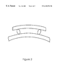
- FIG. 7 is a perspective view of a substrate with an annular ring attached thereto in accordance with the present invention.
- Adding a ring or annular part that compresses the IC in an IC/PC board assembly or that compresses the substrate in an IC package/PC board assembly can increase the expected life of the solder joint in the assembly by a factor of 2 or more.
- the ring ( 506 ) surrounds the IC ( 502 ) (see FIG. 5 a ).
- the ring ( 506 ) surrounds the substrate ( 508 ) in the IC package (see FIG. 5 b ).
- FIG. 4 shows an example embodiment of an annular ring.
- the annular part can be circular, square, or any other shape, as long as the opening in the annular part completely surrounds the outer perimeter of the IC or substrate.
- the ring is made of a material that has a higher coefficient of thermal expansion than the IC, or substrate, that the ring will surround.
- the ring ( 506 ) is constructed such that at an elevated temperature the IC ( 502 ) (see FIG. 5 a ) or substrate ( 508 ) (see FIG. 5 b ) just fits inside the inner diameter of the ring.
- the ring has a gap between the IC or substrate and the inner diameter of the ring at the elevated temperature. This gap is filled with an apoxy or other material, at the elevated temperature, to create a solid contact between the ring and the IC or substrate. The gap allows a larger tolerance for the inner diameter of the ring during the manufacturing process.
- the assembly of the ring and the IC or substrate fit together without any stress. Because the ring has a higher coefficient of thermal expansion than the IC or substrate that it surrounds, the ring will shrink at a faster rate than the IC or substrate for a given temperature change. At room or operating temperature, the ring has compressed the IC or substrate that it surrounds and forced the IC or substrate to change its length more than it would have without the ring attached. By changing the length of the IC or substrate more than it would have without the ring attached for the same temperature change, the change in length of the IC or substrate more closely matches the change in length of the PC board that it is attached to. Because the IC or substrate length change with the ring attached is closer to the PC board length change there is less stress in the solder that forms the joint between the IC or substrate and the PC board, and there is less stress in the PC board.
- the elevated temperature where the ring is assembled to the IC or substrate can be the same temperature used in the soldering process or it can be another temperature.
- the ring has a cross section of 7.5 ⁇ 7.5 mm.
- the substrate is attached to a PC board with 0.9 mm solder balls and subjected to a ⁇ 200 degree C. temperature change.
- the solder ball joint would have an expected increase in life of 2.06 over the same joint without the ring.
- a 200-degree C. temperature change typically corresponds to a standard environmental qualification test.
- the Al 2 O 3 substrate has a coefficient of thermal expansion of 6 ppm/° C. and a modulus of elasticity of 270 ⁇ 10 9 Pa.
- the aluminum ring has a coefficient of thermal expansion of 23.4 ppm/° C. and a modulus of elasticity of 70 ⁇ 10 9 Pa.
- the PC board has a coefficient of thermal expansion of 17.6 ppm/° C.
- Equation 2 gives the total deformation of the substrate.
- Equation 4 gives the deformation of the aluminum ring along one segment of its length.
- the length 702 of the substrate 602 is assumed equal to the length 704 of the ring segment 604 and the corners of the ring 706 are not included (see FIG. 7 ).
- ⁇ FL A r ⁇ E r + ⁇ r ⁇ ⁇ ⁇ ⁇ TL . Equation ⁇ ⁇ 4
- Equation 5 relates the force in the ring segment to the force per unit area (stress) in the Al 2 O 3 substrate. Because there are two ring segments in any section cut, the force in each ring segment is equal to 1 ⁇ 2 the force in the Al 2 O 3 substrate.
- F Pt s ⁇ L 2 . Equation ⁇ ⁇ 5
- Equation 6 is a combination of equations 4 and 5 and gives the total deformation of the ring segment.
- ⁇ Pt s ⁇ L 2 2 ⁇ A r ⁇ E r + ⁇ r ⁇ ⁇ ⁇ ⁇ TL . Equation ⁇ ⁇ 6
- Equation 7 is the solution for P of the combination of equation 3 and equation 6.
- P ( ⁇ s - ⁇ r ) ⁇ ⁇ ⁇ ⁇ T ( t s ⁇ L 2 ⁇ A r ⁇ E r + 1 - v s E s ) . Equation ⁇ ⁇ 7
- the deformation in the Al 2 O 3 substrate, with the ring attached can be calculated using equation 3.
- the length used is the longest or worst case diagonal from the middle of the substrate to the corner of the substrate or 40/square root of 2 which equals 28.3 mm.
- N the number of cycles of temperature change until failure.
- N ring with the ring is 2.06 larger than the life, N no-ring , without the ring.
- the modulus of elasticity for the Al 2 O 3 substrate is 270 ⁇ 10 9 Pa and the ultimate strength of the Al 2 O 3 substrate is 270 ⁇ 10 6 Pa.
- the factor of safety is the maximum allowable stress or strain in a material divided by the actual stress or strain in the material or the strength of the material divided by the stress in the material.
- the factor of safety for the A 1 2 O 3 substrate is given by equation 11.
- F is the force
- A is the area of a ring segment
- P is the stress in the substrate
- t s is the thickness of the substrate
- L is the length of the substrate
- t r is the thickness of the ring segment.
- the factors of safety of 1.41 and 2.5 show that the strain in the Al 2 O 3 substrate and the stress in the aluminum ring are well within reasonable limits.
Abstract
Description


Claims (24)
Priority Applications (6)
| Application Number | Priority Date | Filing Date | Title |
|---|---|---|---|
| US09/369,898 US6320754B1 (en) | 1999-08-06 | 1999-08-06 | Apparatus for the reduction of interfacial stress caused by differential thermal expansion in an integrated circuit package |
| TW089109865A TW497233B (en) | 1999-08-06 | 2000-05-22 | Apparatus for the reduction of interfacial stress caused by differential thermal expansion in an integrated circuit package |
| GB0017054A GB2356084B (en) | 1999-08-06 | 2000-07-11 | Apparatus for the reduction of interfacial stress caused by differential thermal expansion in a integrated circuit package |
| DE10034309A DE10034309B4 (en) | 1999-08-06 | 2000-07-14 | Device for reducing interfacial tensions caused by thermal expansion in a substrate |
| JP2000228296A JP2001085819A (en) | 1999-08-06 | 2000-07-28 | Integrated circuit stress reduction device |
| KR1020000045190A KR100709832B1 (en) | 1999-08-06 | 2000-08-04 | Apparatus for the reduction of interfacial stress caused by differential thermal expansion in an integrated circuit package |
Applications Claiming Priority (1)
| Application Number | Priority Date | Filing Date | Title |
|---|---|---|---|
| US09/369,898 US6320754B1 (en) | 1999-08-06 | 1999-08-06 | Apparatus for the reduction of interfacial stress caused by differential thermal expansion in an integrated circuit package |
Publications (1)
| Publication Number | Publication Date |
|---|---|
| US6320754B1 true US6320754B1 (en) | 2001-11-20 |
Family
ID=23457388
Family Applications (1)
| Application Number | Title | Priority Date | Filing Date |
|---|---|---|---|
| US09/369,898 Expired - Fee Related US6320754B1 (en) | 1999-08-06 | 1999-08-06 | Apparatus for the reduction of interfacial stress caused by differential thermal expansion in an integrated circuit package |
Country Status (6)
| Country | Link |
|---|---|
| US (1) | US6320754B1 (en) |
| JP (1) | JP2001085819A (en) |
| KR (1) | KR100709832B1 (en) |
| DE (1) | DE10034309B4 (en) |
| GB (1) | GB2356084B (en) |
| TW (1) | TW497233B (en) |
Cited By (5)
| Publication number | Priority date | Publication date | Assignee | Title |
|---|---|---|---|---|
| US20030116860A1 (en) * | 2001-12-21 | 2003-06-26 | Biju Chandran | Semiconductor package with low resistance package-to-die interconnect scheme for reduced die stresses |
| US20040240188A1 (en) * | 2003-05-28 | 2004-12-02 | Cromwell Stephen Daniel | Protective coating for attach hardware for circuits |
| US7235886B1 (en) * | 2001-12-21 | 2007-06-26 | Intel Corporation | Chip-join process to reduce elongation mismatch between the adherents and semiconductor package made thereby |
| US20120081872A1 (en) * | 2010-09-30 | 2012-04-05 | Alcatel-Lucent Canada Inc. | Thermal warp compensation ic package |
| CN108550559A (en) * | 2018-05-28 | 2018-09-18 | 北京比特大陆科技有限公司 | Cooling fin, chip assembly and circuit board |
Families Citing this family (2)
| Publication number | Priority date | Publication date | Assignee | Title |
|---|---|---|---|---|
| DE10340866A1 (en) * | 2003-09-04 | 2005-03-31 | Siemens Ag | Method for fixing element-group on carrier layer e.g. for miniaturization of communication devices, involves joining first and second elements together at an initial temperature, so that a mutual mechanical force is exerted |
| DE102018104521B4 (en) | 2018-02-28 | 2022-11-17 | Rogers Germany Gmbh | metal-ceramic substrates |
Citations (13)
| Publication number | Priority date | Publication date | Assignee | Title |
|---|---|---|---|---|
| US4437718A (en) * | 1981-12-17 | 1984-03-20 | Motorola Inc. | Non-hermetically sealed stackable chip carrier package |
| EP0452752A2 (en) | 1990-04-16 | 1991-10-23 | Fujitsu Limited | Chip carrier for enabling production of high performance microwave semiconductor device by disposing semiconductor chip thereon |
| GB2276977A (en) | 1992-12-08 | 1994-10-12 | Hughes Aircraft Co | Reducing thermal stress in I.C. chip mountings |
| US5455387A (en) * | 1994-07-18 | 1995-10-03 | Olin Corporation | Semiconductor package with chip redistribution interposer |
| US5570274A (en) * | 1993-11-29 | 1996-10-29 | Nec Corporation | High density multichip module packaging structure |
| US5844319A (en) * | 1997-03-03 | 1998-12-01 | Motorola Corporation | Microelectronic assembly with collar surrounding integrated circuit component on a substrate |
| US5868887A (en) | 1996-11-08 | 1999-02-09 | W. L. Gore & Associates, Inc. | Method for minimizing warp and die stress in the production of an electronic assembly |
| US5892289A (en) * | 1996-04-22 | 1999-04-06 | Nec Corporation | Bare chip mounting structure and manufacturing method therefor |
| US5909057A (en) * | 1997-09-23 | 1999-06-01 | Lsi Logic Corporation | Integrated heat spreader/stiffener with apertures for semiconductor package |
| US5936304A (en) | 1997-12-10 | 1999-08-10 | Intel Corporation | C4 package die backside coating |
| US5973404A (en) * | 1996-03-07 | 1999-10-26 | Micron Technology, Inc. | Underfill of bumped or raised die using a barrier adjacent to the sidewall of semiconductor device |
| US6011304A (en) * | 1997-05-05 | 2000-01-04 | Lsi Logic Corporation | Stiffener ring attachment with holes and removable snap-in heat sink or heat spreader/lid |
| US6081416A (en) * | 1998-05-28 | 2000-06-27 | Trinh; Hung | Lead frames for mounting ceramic electronic parts, particularly ceramic capacitors, where the coefficient of thermal expansion of the lead frame is less than that of the ceramic |
Family Cites Families (3)
| Publication number | Priority date | Publication date | Assignee | Title |
|---|---|---|---|---|
| JPS55107247A (en) * | 1979-02-09 | 1980-08-16 | Matsushita Electric Ind Co Ltd | Hybrid integrated circuit |
| JPS58138050A (en) * | 1982-02-10 | 1983-08-16 | Sumitomo Electric Ind Ltd | Manufacture of semiconductor device |
| US5877070A (en) * | 1997-05-31 | 1999-03-02 | Max-Planck Society | Method for the transfer of thin layers of monocrystalline material to a desirable substrate |
-
1999
- 1999-08-06 US US09/369,898 patent/US6320754B1/en not_active Expired - Fee Related
-
2000
- 2000-05-22 TW TW089109865A patent/TW497233B/en not_active IP Right Cessation
- 2000-07-11 GB GB0017054A patent/GB2356084B/en not_active Expired - Fee Related
- 2000-07-14 DE DE10034309A patent/DE10034309B4/en not_active Expired - Fee Related
- 2000-07-28 JP JP2000228296A patent/JP2001085819A/en not_active Withdrawn
- 2000-08-04 KR KR1020000045190A patent/KR100709832B1/en not_active IP Right Cessation
Patent Citations (13)
| Publication number | Priority date | Publication date | Assignee | Title |
|---|---|---|---|---|
| US4437718A (en) * | 1981-12-17 | 1984-03-20 | Motorola Inc. | Non-hermetically sealed stackable chip carrier package |
| EP0452752A2 (en) | 1990-04-16 | 1991-10-23 | Fujitsu Limited | Chip carrier for enabling production of high performance microwave semiconductor device by disposing semiconductor chip thereon |
| GB2276977A (en) | 1992-12-08 | 1994-10-12 | Hughes Aircraft Co | Reducing thermal stress in I.C. chip mountings |
| US5570274A (en) * | 1993-11-29 | 1996-10-29 | Nec Corporation | High density multichip module packaging structure |
| US5455387A (en) * | 1994-07-18 | 1995-10-03 | Olin Corporation | Semiconductor package with chip redistribution interposer |
| US5973404A (en) * | 1996-03-07 | 1999-10-26 | Micron Technology, Inc. | Underfill of bumped or raised die using a barrier adjacent to the sidewall of semiconductor device |
| US5892289A (en) * | 1996-04-22 | 1999-04-06 | Nec Corporation | Bare chip mounting structure and manufacturing method therefor |
| US5868887A (en) | 1996-11-08 | 1999-02-09 | W. L. Gore & Associates, Inc. | Method for minimizing warp and die stress in the production of an electronic assembly |
| US5844319A (en) * | 1997-03-03 | 1998-12-01 | Motorola Corporation | Microelectronic assembly with collar surrounding integrated circuit component on a substrate |
| US6011304A (en) * | 1997-05-05 | 2000-01-04 | Lsi Logic Corporation | Stiffener ring attachment with holes and removable snap-in heat sink or heat spreader/lid |
| US5909057A (en) * | 1997-09-23 | 1999-06-01 | Lsi Logic Corporation | Integrated heat spreader/stiffener with apertures for semiconductor package |
| US5936304A (en) | 1997-12-10 | 1999-08-10 | Intel Corporation | C4 package die backside coating |
| US6081416A (en) * | 1998-05-28 | 2000-06-27 | Trinh; Hung | Lead frames for mounting ceramic electronic parts, particularly ceramic capacitors, where the coefficient of thermal expansion of the lead frame is less than that of the ceramic |
Cited By (9)
| Publication number | Priority date | Publication date | Assignee | Title |
|---|---|---|---|---|
| US20030116860A1 (en) * | 2001-12-21 | 2003-06-26 | Biju Chandran | Semiconductor package with low resistance package-to-die interconnect scheme for reduced die stresses |
| US20050116329A1 (en) * | 2001-12-21 | 2005-06-02 | Intel Corporation | Semiconductor package with low resistance package-to-die interconnect scheme for reduced die stresses |
| US7122403B2 (en) | 2001-12-21 | 2006-10-17 | Intel Corporation | Method of interconnecting die and substrate |
| US7235886B1 (en) * | 2001-12-21 | 2007-06-26 | Intel Corporation | Chip-join process to reduce elongation mismatch between the adherents and semiconductor package made thereby |
| CN100431396C (en) * | 2001-12-21 | 2008-11-05 | 英特尔公司 | Chip-join process to reduce elongation mismatch between the adherents and semiconductor package made thereby |
| US20040240188A1 (en) * | 2003-05-28 | 2004-12-02 | Cromwell Stephen Daniel | Protective coating for attach hardware for circuits |
| US20120081872A1 (en) * | 2010-09-30 | 2012-04-05 | Alcatel-Lucent Canada Inc. | Thermal warp compensation ic package |
| US8912449B2 (en) | 2010-09-30 | 2014-12-16 | Alcatel Lucent | Thermal warp compensation IC package |
| CN108550559A (en) * | 2018-05-28 | 2018-09-18 | 北京比特大陆科技有限公司 | Cooling fin, chip assembly and circuit board |
Also Published As
| Publication number | Publication date |
|---|---|
| TW497233B (en) | 2002-08-01 |
| KR100709832B1 (en) | 2007-04-23 |
| JP2001085819A (en) | 2001-03-30 |
| GB0017054D0 (en) | 2000-08-30 |
| KR20010021214A (en) | 2001-03-15 |
| DE10034309B4 (en) | 2004-03-04 |
| GB2356084A (en) | 2001-05-09 |
| DE10034309A1 (en) | 2001-04-05 |
| GB2356084B (en) | 2003-10-22 |
Similar Documents
| Publication | Publication Date | Title |
|---|---|---|
| US6111322A (en) | Semiconductor device and manufacturing method thereof | |
| CA2118649C (en) | Interconnection structure of electronic parts | |
| US6049128A (en) | Semiconductor device | |
| KR100360146B1 (en) | Semiconductor device | |
| AU603450B2 (en) | Mounting for printed circuit forming a heat sink with controlled expansion | |
| US5604978A (en) | Method for cooling of chips using a plurality of materials | |
| US4654966A (en) | Method of making a dimensionally stable semiconductor device | |
| US20080253098A1 (en) | Damage Prevention Interposer for Electronic Package and Electronic Interconnect Structure | |
| US6365441B1 (en) | Partial underfill for flip-chip electronic packages | |
| US5901043A (en) | Device and method for reducing thermal cycling in a semiconductor package | |
| US8912449B2 (en) | Thermal warp compensation IC package | |
| US6703560B2 (en) | Stress resistant land grid array (LGA) module and method of forming the same | |
| US6320754B1 (en) | Apparatus for the reduction of interfacial stress caused by differential thermal expansion in an integrated circuit package | |
| US7898076B2 (en) | Structure and methods of processing for solder thermal interface materials for chip cooling | |
| US7268427B2 (en) | Semiconductor package, printed board mounted with the same, and electronic apparatus having the printed board | |
| US20070228530A1 (en) | Heat conductive bonding material, semiconductor package, heat spreader, semiconductor chip and bonding method of bonding semiconductor chip to heat spreader | |
| JP2000022034A (en) | Connection structure of electronic circuit device | |
| US20030202332A1 (en) | Second level packaging interconnection method with improved thermal and reliability performance | |
| US6020638A (en) | Packaging structure of BGA type semiconductor device mounted on circuit substrate | |
| JP3399418B2 (en) | Mounting structure of surface mount type semiconductor device | |
| EP1675173A2 (en) | Epoxy-solder thermally conductive structure for an integrated circuit | |
| EP4120335A1 (en) | Heat sink integrated insulating circuit board | |
| Xie et al. | Solder joint reliability of double-side mounted DDR modules for consumer and automotive applications | |
| US20230253290A1 (en) | Thermal spreader for thermal dissipation in space and other applications | |
| JP4162506B2 (en) | Electronic component cooling structure and semiconductor module |
Legal Events
| Date | Code | Title | Description |
|---|---|---|---|
| AS | Assignment |
Owner name: AGILENT TECHNOLOGIES, CALIFORNIA Free format text: ASSIGNMENT OF ASSIGNORS INTEREST;ASSIGNORS:DAUKSHER, WALTER J.;ENGEL, PEDRO F.;REEL/FRAME:010436/0420 Effective date: 19990806 |
|
| AS | Assignment |
Owner name: HEWLETT-PACKARD COMPANY, COLORADO Free format text: MERGER;ASSIGNOR:HEWLETT-PACKARD COMPANY;REEL/FRAME:010759/0049 Effective date: 19980520 |
|
| AS | Assignment |
Owner name: AGILENT TECHNOLOGIES INC, CALIFORNIA Free format text: ASSIGNMENT OF ASSIGNORS INTEREST;ASSIGNOR:HEWLETT-PACKARD COMPANY;REEL/FRAME:010977/0540 Effective date: 19991101 |
|
| FEPP | Fee payment procedure |
Free format text: PAYOR NUMBER ASSIGNED (ORIGINAL EVENT CODE: ASPN); ENTITY STATUS OF PATENT OWNER: LARGE ENTITY |
|
| FPAY | Fee payment |
Year of fee payment: 4 |
|
| AS | Assignment |
Owner name: AVAGO TECHNOLOGIES GENERAL IP PTE. LTD., SINGAPORE Free format text: ASSIGNMENT OF ASSIGNORS INTEREST;ASSIGNOR:AGILENT TECHNOLOGIES, INC.;REEL/FRAME:017207/0020 Effective date: 20051201 |
|
| REMI | Maintenance fee reminder mailed | ||
| LAPS | Lapse for failure to pay maintenance fees | ||
| STCH | Information on status: patent discontinuation |
Free format text: PATENT EXPIRED DUE TO NONPAYMENT OF MAINTENANCE FEES UNDER 37 CFR 1.362 |
|
| FP | Lapsed due to failure to pay maintenance fee |
Effective date: 20091120 |
|
| AS | Assignment |
Owner name: AVAGO TECHNOLOGIES GENERAL IP (SINGAPORE) PTE. LTD Free format text: CORRECTIVE ASSIGNMENT TO CORRECT THE NAME OF THE ASSIGNEE PREVIOUSLY RECORDED ON REEL 017207 FRAME 0020. ASSIGNOR(S) HEREBY CONFIRMS THE ASSIGNMENT;ASSIGNOR:AGILENT TECHNOLOGIES, INC.;REEL/FRAME:038633/0001 Effective date: 20051201 |