US6304357B1 - Optical receiver - Google Patents

Optical receiver Download PDF

Info

Publication number
US6304357B1
US6304357B1 US09/041,973 US4197398A US6304357B1 US 6304357 B1 US6304357 B1 US 6304357B1 US 4197398 A US4197398 A US 4197398A US 6304357 B1 US6304357 B1 US 6304357B1
Authority
US
United States
Prior art keywords
signal
voltage
amplifier
optical
output
Prior art date
Legal status (The legal status is an assumption and is not a legal conclusion. Google has not performed a legal analysis and makes no representation as to the accuracy of the status listed.)
Expired - Fee Related
Application number
US09/041,973
Inventor
Kenichi Ohhata
Ryoji Takeyari
Toru Masuda
Katsuyoshi Washio
Yasushi Hatta
Current Assignee (The listed assignees may be inaccurate. Google has not performed a legal analysis and makes no representation or warranty as to the accuracy of the list.)
Hitachi Ltd
Japan Display Inc
Original Assignee
Hitachi Device Engineering Co Ltd
Hitachi Ltd
Priority date (The priority date is an assumption and is not a legal conclusion. Google has not performed a legal analysis and makes no representation as to the accuracy of the date listed.)
Filing date
Publication date
Application filed by Hitachi Device Engineering Co Ltd, Hitachi Ltd filed Critical Hitachi Device Engineering Co Ltd
Assigned to HITACHI DEVICE ENGINEERING CO., LTD., HITACHI, LTD. reassignment HITACHI DEVICE ENGINEERING CO., LTD. ASSIGNMENT OF ASSIGNORS INTEREST (SEE DOCUMENT FOR DETAILS). Assignors: HATTA, YASUSHI, MASUDA, TORU, NASHIO, KATSUYOSHI, OHHATA, KENICHI, TAKEYARI, RYOJI
Priority to US09/946,450 priority Critical patent/US6658217B2/en
Application granted granted Critical
Publication of US6304357B1 publication Critical patent/US6304357B1/en
Anticipated expiration legal-status Critical
Expired - Fee Related legal-status Critical Current

Links

Images

Classifications

    • HELECTRICITY
    • H04ELECTRIC COMMUNICATION TECHNIQUE
    • H04BTRANSMISSION
    • H04B10/00Transmission systems employing electromagnetic waves other than radio-waves, e.g. infrared, visible or ultraviolet light, or employing corpuscular radiation, e.g. quantum communication
    • H04B10/60Receivers
    • H04B10/66Non-coherent receivers, e.g. using direct detection
    • H04B10/69Electrical arrangements in the receiver
    • H04B10/693Arrangements for optimizing the preamplifier in the receiver
    • H04B10/6932Bandwidth control of bit rate adaptation
    • HELECTRICITY
    • H04ELECTRIC COMMUNICATION TECHNIQUE
    • H04BTRANSMISSION
    • H04B10/00Transmission systems employing electromagnetic waves other than radio-waves, e.g. infrared, visible or ultraviolet light, or employing corpuscular radiation, e.g. quantum communication
    • H04B10/60Receivers
    • H04B10/66Non-coherent receivers, e.g. using direct detection
    • H04B10/69Electrical arrangements in the receiver
    • H04B10/693Arrangements for optimizing the preamplifier in the receiver
    • H04B10/6933Offset control of the differential preamplifier
    • HELECTRICITY
    • H04ELECTRIC COMMUNICATION TECHNIQUE
    • H04BTRANSMISSION
    • H04B10/00Transmission systems employing electromagnetic waves other than radio-waves, e.g. infrared, visible or ultraviolet light, or employing corpuscular radiation, e.g. quantum communication
    • H04B10/60Receivers
    • H04B10/66Non-coherent receivers, e.g. using direct detection
    • H04B10/69Electrical arrangements in the receiver
    • H04B10/695Arrangements for optimizing the decision element in the receiver, e.g. by using automatic threshold control

Definitions

  • the present invention relates generally to optical receivers, and more particularly, to an optical receiver that adjusts the output swing in response to a change in the signal input, with high sensitivity and over a wide dynamic range.
  • FIG. 1 shows a conventional optical receiver used in an optical transmission system for a main line having a maximum transmission distance of 100 km, for example.
  • a receiving element for example, an avalanche photodiode APD
  • receives an input optical signal and outputs an optical ON/OFF rectangular pattern (corresponding to the binary signals “1” and “0”, respectively) for every time period ⁇ t, at a data rate of 1 bit.
  • FIGS. 2 ( a )- 2 ( c ) illustrate a decision operation of the optical receiver for 6 bits of the input optical signal.
  • an electron-hole pair induces avalanche multiplication, as caused by the optical signal, to amplify the signal current (FIG. 2 ( a )).
  • This amplification makes it possible to detect even a weak optical signal.
  • the current signal output from the APD is converted to a voltage signal VPRE by a preamplifier PRE (FIG. 2 ( b )).
  • This signal VPRE is further amplified by an automatic-gain-control amplifier AGC (also known as a “gain-controllable amplifier”), and the resulting signal VAGC is input to a decision circuit DEC (FIG. 2 ( c )).
  • the swing of the output signal VAGC of the AGC amplifier is held at a substantially constant level by the automatic gain control function of the AGC amplifier. As a result, the decision made by the decision circuit is stabilized.
  • the datq are output in synchronism with a clock signal CLK by deciding that the output signal VAGC of the AGC amplifier is high (“1”) if the output signal VAGC is higher than a reference voltage VTH (also called VTH(DEC) below), or low (“0”) if lower than the reference voltage VTH.
  • the clock signal CLK may be prepared from the output signal VAGC by a clock-extraction circuit CEXT.
  • a voltage signal V PRE from the preamplifier PRE is amplified by three stages of amplifiers, including gain-controllable amplifiers A 1 and A 2 , and a constant-gain amplifier A 3 . Then, the output of the constant-gain amplifier A 3 , which has a swing V A3 , is input to a peak detector PD. This peak detector PD generates a DC voltage V 3 based upon the swing V A3 using a capacitor C PD .
  • a reference circuit REF generates the nominal value of the peak voltage VN (the “nominal voltage swing”). This nominal value VN is adjusted by a variable voltage source P connected to the reference circuit REF.
  • the voltage V 3 and the nominal value VN are compared so that voltages V GC1 and V GC2 for controlling the gains of the amplifiers A 1 and A 2 are set according to the difference (i.e., the deviation of the signal swing from the nominal voltage swing).
  • the difference i.e., the deviation of the signal swing from the nominal voltage swing.
  • a voltage signal VAGC having a swing of 500 mV is output at a rate of 13 Gb/sec for an input signal having a swing of either 10 mV or 300 mV.
  • These output signals are output from two output buffers OB so as to be input to the decision circuit DEC and the clock-extraction circuit respectively.
  • the AGC amplifier of FIG. 3 is further equipped with an offset-control circuit OC (having external capacitors C OC ) for controlling the offsets of the amplifiers A 1 , A 2 , and A 3 .
  • an offset-control circuit OC having external capacitors C OC ) for controlling the offsets of the amplifiers A 1 , A 2 , and A 3 .
  • the decision circuit DEC decides whether the signal V AGC is “1” or “0”, by employing a voltage between the upper and lower ends of the swing voltage of the output signal as the reference voltage VTH(DEC).
  • FIG. 4 illustrates how the optical signal, as transmitted from the optical transmission passage (optical fibers, for example), is converted to a voltage signal by the preamplifier PRE.
  • the abscissa indicates the signal voltage value
  • the ordinate indicates the frequency with which the signal is generated at a predetermined voltage level.
  • the “1” signal may have a wider voltage distribution than that of the “0” signal.
  • the voltage distribution of a “1” signal takes the shape (illustrated by a broken curve in FIG. 4) in which the solid curve of FIG. 4 is depressed in the ordinate direction. This shape is especially prominent when either an APD or an erbium-doped fiber amplifier (EDFA) in combination with a PIN junction photodetector (or PIN diode) is used as the optical receiving element. See “Optical Fiber Communication Technique”, published by NIKKAN KOGYO SHINBUN SHA.
  • Voltages signals that do not exceed the reference voltage V th (A) are decided to be “0” signals even if they are “1” signals in fact, due to this error.
  • the probability for these erroneous decisions is the “error rate” of the decision circuit.
  • the error rate is defined as the ratio of the area of the region under the broken-line curve to the left of V th (A), to the entire area under the broken-line curve, which represents the voltage distribution of the actual “1” signal.
  • the error rate cannot be zero when the voltage distribution curve (broken curve) of the “1” signals and the voltage distribution curve (solid curve) of the “0” signals overlap.
  • the error rate can be reduced when the threshold voltage is considerably shifted toward V 0 .
  • a threshold voltage V th (B) can be set at a point where the voltage distribution curve of the “1” signal and the voltage distribution curve of the “0” signal intersect.
  • the error rate can be reduced as low as the area ratio shown hatched in FIG. 4 .
  • the total error rate is reduced compared with that under Vth(A).
  • the distribution of the signal voltage extends wider than the magnitude (V 1 ⁇ V 0 ) of the signal anyway, so that the error rate cannot be completely reduced to 0 irrespective of where the reference voltage is set.
  • the reference voltage is set within a range that allows and achieves a remarkably low constant error rate (e.g., 10 ⁇ 12 ). Then, the transmission errors that do occur can be detected and corrected with an error correction code.
  • FIG. 5 schematically illustrates the relationship between the set range of the reference voltage and the optical signal intensity, with an error rate considered with an APD or the combination of an EDFA and PIN diode as the optical receiving element.
  • the “1” signal indicates a wider voltage distribution than that of the “0” signal, as described above, so that the set range of the reference voltage is offset toward the “0” signal peak.
  • the optical signal intensity becomes lower, the set range of the reference voltage grows gradually narrower until the desired error rate cannot be achieved at all.
  • the optical signal intensity at this point (indicated by Pmin 0 ) is called the “minimum receiver sensitivity”.
  • Pmin 0 represents the point below which the overlap of the “1” and “0” curves (which represents the error rate) is too great for the desired error rate to be achieved.
  • the optical receiver To cover applications for various transmission distances, a wide input dynamic range is required, even for a receiver for a main line.
  • the optical signal attenuation through the optical fibers is so low that an intense optical signal is input to the receiver.
  • the transmission distance is long, on the other hand, the input optical signal is very weak.
  • the optical receiver must be capable of handling both cases.
  • FIGS. 6 ( a )- 6 ( c ) illustrate response waveforms for the receiver when a strong optical signal is input.
  • the intensity of the optical signal is high, the output current of the optical receiving element rises, to increasing the output swing of the preamplifier.
  • the output swing of the preamplifier becomes excessively large, however, a signal change occurs before the output signal reaches a steady value, as illustrated, so that the output waveform partially takes a triangular shape.
  • the partial triangular shape results because the changing rate of the output VPRE of the preamplifier has an upper limit (dV/dt) called the “slew rate”. If the slew rate of the AGC amplifier is sufficiently higher than that of the preamplifier, the output signal of the AGC amplifier has a similar waveform as that of the VPRE.
  • the first bit (left side) or the fifth bit (second bit from right side) are erroneously decided no matter where the reference voltage VTH(DEC) might be set, because the preferable VTH(DEC) for deciding the first bit as “0” cannot but be too high for the fifth bit to be decided as “1”, and the preferable VTH(DEC) for deciding the fifth bit as “1” cannot but be too low for the first bit to be decided as “0”, Vth(A). Since the output VPRE of the preamplifier has a large swing, moreover, the voltage to be applied to a transistor of the output stage of the preamplifier rises so high as to make it necesasary to use a transistor with a high breakdown voltage.
  • FIG. 7 illustrates a construction of an optical receiver disclosed in this article.
  • This circuit is employed in a local area network (LAN), for example, and has a transmission distance as short as several Km at most. Therefore, the APD is replaced by a PIN photodiode.
  • the AGC amplifier is also replaced, by a limiting amplifier LA.
  • the gain of the limiting amplifier LA is set at a remarkably high value so that the output signal is clamped to a predetermined voltage range, to limit the swing whenever the output swing rises above a desired value.
  • the reference voltage VTH(LA) is controlled by the reference voltage control circuit VCNT to be just intermediate between the high voltage (corresponding to “1”, for example) and the low voltage (corresponding to “0”, for example) of the input signal.
  • the input signal and VTH(LA) are compared so that a constant voltage VLA( 1 ) is output irrespective of the swing of the input signal if the input signal is higher than VTH(LA), but a constant voltage VLA( 0 ) is output irrespective of the input signal swing if the input signal is lower than VTH(LA).
  • the gain of the limiting amplifier LA is set at about 60 dB so that an output signal of constant swing is achieved over a wide range of input signals, from several mV to about 1 V.
  • the gain of the limiting amplifier is so high that the gain (i.e., the ratio between the output voltage and the input current, also called the “transimpedance”) of the preamplifier need not be raised so high.
  • the swing of the output VPRE of the preamplifier is not so large as that of the aforementioned construction, so that the signal is neither distorted nor becomes a triangular wave, as illustrated in FIG. 6 ( b ). This raises no problem due to the slew rate.
  • FIG. 8 illustrates a set range of the reference voltage VTH(LA) of the limiting amplifier LA in the preamplifier output VPRE. Because an optical receiving element having an amplifying function is used, the “1” signal indicates a wider voltage distribution than that of the “0” signal, and the set range of the reference voltage is offset towards the “0” signal side, as before.
  • the output (VLA) of the limiting amplifier LA is derived by extracting a signal represented by VTH(LA) ⁇ several mV from the VPRE and by amplifying it (a voltage width of several mV being indicated by a double curve).
  • the VTH(LA) is set just intermediate between the VPRE(0) and the VPRE(1), such that the VTH(LA) deviates from the set range of the reference value for a region where the optical signal intensity is Pmin 1 or less.
  • the minimum receiver sensitivity is at Pmin 1 , which is a lower sensitivity (i.e., Pmin 1 is>than Pmin 0 ) than that of the construction of FIG. 1 .
  • the PIN diode Since the PIN diode has no amplifying action, the “1” signal exhibits the same voltage distribution as that of the “0” signal, so that the aforementioned problem does not occur even if the VTH(LA) is set just intermediate between the VPRE( 0 ) and the VPRE( 1 ).
  • the reference voltage VTH(LA) of the limiting amplifier LA can be adjusted, not to the center of the VPRE, but towards the side of the “0” level.
  • this method is extremely difficult to realize, because the intensity of the optical signal to be adjusted is weak (especially within a range less than Pmin 1 ), and because the reference voltage VTH(LA) must be precisely adjusted under the condition of a small swing of the VPRE. Since the intensity of the optical signal fluctuates by the degradation in the characteristics of the transmitter or the optical fibers, it is necessary to periodically readjust the reference voltage VTH(LA). Thus, it has been impossible to use a wide dynamic range receiver in a LAN, as disclosed in this article, as has been used for long distance transmission.
  • Japanese Patent Laid Open No. 93-259752 (Tokukai-Hei 05-259752), which discloses an improved technique for setting a reference potential of the discrimination (decision) circuit, according to which the circuit decides a voltage signal input thereto to be either “0” or “1”, and in Japanese Patent Laid Open No. 96-139526 (Tokukai-Hei 08-139526), No. 95-193437 (Tokukai-Hei 07-193437), No. 95-38342 (Tokukai-Hei 07-38342), and No. 93-67930 (Tokukai-Hei 05-67930), which disclose improved circuitries for setting the gain of the preamplifier.
  • Japanese Patent Laid Open No. 97-246879 (Tokukai-Hei 09-246879), and No. 93-218758 (Tokukai-Hei 05-218758) disclose techniques for suppressing deterioration of the width of the voltage pulse in the optical receiver, but the key techniques for solving the problems illustrated in FIGS. 1 and 7, discussed above, are not disclosed.
  • An object of the present invention is to provide an optical receiver having a high sensitivity and a wide dynamic range.
  • the invention provides an opticalreceiver for converting an optical signal into an electrical signal, including an optical receiving element (photoelectric converter) for converting the optical signal into a current signal, a preamplifier for converting the current signal output by the photoelectric converter into a voltage signal, an amplifier having a limiting function for linearly amplifying the voltage signal when the difference between the voltage signal and a reference voltage is smaller than a predetermined voltage, and for limitedly amplifying the voltage signal when the difference is larger than the predetermined voltage, and an automatic-gain-control amplifier for amplifying the output of the amplifier having the limiting function, to produce a signal having a constant swing.
  • the amplifier having the limiting function and the circuit stage performing its function are referred to below as the “present limiting amplifier” and the “present limiting amplification stage”, respectively.
  • the predetermined voltage at which the present limiting amplifier starts its limited amplification is desirably set larger than the difference between the output signal of the preamplifier in the minimum receiver sensitivity and the reference voltage.
  • the output signal by the preamplifier in the minimum receiver sensitivity is determined at a desired error rate by the photoelectric converter and the preamplifier.
  • the output signal swing of the amplifier having the limiting function is desirably restricted to satisfy the following formula within a desired dynamic range of the optical signal:
  • ⁇ VAWL is the output signal swing of the amplifier having the limiting function
  • ⁇ t is the time period to be occupied by an optical signal representing 1 bit
  • Rs is the slew rate of the amplifier having the limiting function.
  • the photoelectric converter is preferably constructed of an avalanche photodiode APD or an erbium-doped fiber amplifier EDFA and a PIN photodiode in combination, so that the minimum receiver sensitivity can be improved.
  • the amplifier with the limiting function linearly amplifies the voltage signal VPRE according to the optical signal.
  • the AGC amplifier disposed at the next stage thereto amplifies the output AWL of the amplifier with the limiting function, and the AGC amplifier provides its output voltage signal VAGC to the decision circuit.
  • the decision circuit sets its reference voltage to decide whether the input signal VAGC is “1” or “0”, corresponding to the signal swing of the VAGC (the voltage difference between the signals of “1” and “0”).
  • the linear amplifications of the voltage signal by the amplifier with the limiting function and the AGC amplifier enable the decision circuit to set its reference voltage to an optimum point, even if the optical receiver accepts fairly weak optical signals.
  • the amplifier with the limiting function acts to limit the output signal swing so as to prevent the output signal of the preamplifier from distorting and to suppress an increase of the error rate.
  • an optical transmission system terminal unit or an optical transmission system includes, in combination, an optical receiver including an optical receiving element (photoelectric converter), a first amplifier (which may be a preamplifier) for converting a current signal output from the optical receiving element into a voltage signal, a second amplifier (which may be a gain-controllable amplifier or an AGC amplifier) for reducing the swing dispersion of the voltage signal output from the first amplifier, a decision circuit for processing (or deciding) the voltage signal output from the second amplifier, and a third amplifier disposed between the first amplifier and the second amplifier.
  • the following functions are required for the third amplifier mentioned above.
  • One function is to set its output signal swing (like ⁇ VAWL in FIG. 9) smaller than the product of the slew rate of the third amplifier and the time period occupied by one bit of an optical signal.
  • the third amplifier Another function required for the third amplifier is to amplify the voltage signal input from the first amplifier thereto when the voltage signal has a smaller swing than a predetermined voltage swing. This function is important for detecting the input signal of an especially minute swing.
  • the linearly amplified range of the third amplifier is set to be wider than that of the limiting amplifier of the prior art. Generally, the gain drops if the linear amplification range is extended, but the third amplifier is utilized in combination with the second amplifier at a downstream stage, so that no practical problem arises.
  • the amplifier with the limiting function acts as a linear amplification so that the reference value of the decision circuit can be set to the optimum point by executing a further linear amplification in the AGC amplifier at the downstream stage.
  • the amplifier with the limiting function performs a limiting action to prevent the output signal swing of the preamplifier from being distorted, which would increase the error rate.
  • the optical receiver has a high sensitivity and a wide dynamic range.
  • FIG. 1 schematically illustrates a conventional optical receiver
  • FIGS. 2 ( a )- 2 ( c ) illustrate the relationships between an optical signal input and the voltage output of the preamplifier and the AGC amplifier of the circuit shown in FIG. 1;
  • FIG. 3 illustrates details of the AGC amplifier of the circuit shown in FIG. 1;
  • FIG. 4 illustrates the error rate of “1” ⁇ “0” signal decision-making
  • FIG. 5 illustrates the setting of a range of a reference voltage above the minimum receiver sensitivity, for the circuit shown in FIG. 1;
  • FIGS. 6 ( a )- 6 ( c ) illustrate waveform distortions due to slew rate
  • FIG. 7 illustrates another conventional optical receiver
  • FIG. 8 illustrates the setting of a range of a reference voltage above a minimum receiver sensitivity for the circuit shown in FIG. 7;
  • FIG. 9 schematically illustrates an optical receiver constructed according to the teachings of the present invention.
  • FIG. 10 illustrates the setting of a range of a reference voltage for the circuit shown in FIG. 9;
  • FIGS. 11 ( a )- 11 ( f ) compare various output signals of the circuit shown in FIG. 7 with those of the circuit shown in FIG. 9;
  • FIG. 12 illustrates more detailed circuitry of the circuit shown in FIG. 9;
  • FIG. 13 shows an example of an amplifier employed in the circuit of FIG. 9;
  • FIG. 14 shows an example of another amplifier that may be used in the circuit of FIG. 9;
  • FIG. 15 illustrates yet another amplifier that may be used in the circuit of FIG. 9;
  • FIG. 16 illustrates an example of a preamplifier that may be used in the circuit of FIG. 9;
  • FIG. 17 illustrates another example of a preamplifier that may be used in the circuit of FIG. 9;
  • FIG. 18 illustrates an example of an AGC amplifier that may be used in the circuit of FIG. 9;
  • FIG. 19 illustrates an example of a reference voltage generator that can be used in the circuit of FIG. 9;
  • FIG. 20 illustrates another example of a reference voltage generator that can be used in the circuit of FIG. 9;
  • FIG. 21 illustrates another embodiment of an optical receiver constructed according to the teachings of the present invention.
  • FIGS. 22 ( a )- 22 ( b ) plot the relationships between the output signal swing and the input current of the photoelectric converter shown in the circuit of FIG. 21;
  • FIG. 23 illustrates another embodiment detailing the circuit shown in FIG. 9;
  • FIG. 24 illustrates an optical communication system employing the optical receiver of the present invention.
  • FIGS. 25 ( a )-( c ) illustrate waveforms of a voltage signal transmitted through the circuit of the optical receiver shown in FIG. 24 .
  • FIG. 9 illustrates fundamental features of a preferred embodiment of the present invention.
  • the construction shown in FIG. 9 differs from that of FIG. 1 by including an amplifier with a limiting function AWL and a reference voltage generator VRG between the preamplifier PRE and the gain-controllable amplifier AGC.
  • both have an amplifier with a limiting function for receiving the output of the preamplifier PRE, as well as circuitry for receiving the preamplifier output and providing the amplifier with the limiting function with a reference voltage.
  • the amplifier AWL of FIG. 9 provides a linear amplification to an input signal that has a small swing, but the limiting amplifier LA of FIG. 7 does not.
  • the amplifier AWL of the present invention acts as a linear amplifier that holds the output swing generally at a constant value by a limiting function only when the output swing exceeds the constant value.
  • the reference voltage Vref of the amplifier AWL is preferably set just at the center between the preamplifier output signals VPRE(0) and VPRE(1), both of which are illustrated by broken curves.
  • the linear amplification range (or the ordinate width, as defined by thick oblique curves) of the AWL is far wider (e.g., several hundreds mV) than that of the limiting amplifier of the prior art.
  • the optical signal intensity is linearly amplified to output a voltage signal VAWL at the minimum receiver sensitivity Pmin 0 , as illustrated in FIG. 10 .
  • the reference voltage of the decision circuit can be set to the optimum point (defined by the voltage (value) along the axis of VPRE within the hatched region of FIG. 10) for the optical signal intensity.
  • the output voltage swing of the VAWL is limited or suppressed to a predetermined value irrespective of the magnitude of VPRE, so that the output signal swing of the AWL does not become excessive.
  • waveform distortions caused by the slew rate can be suppressed to extend the dynamic range of the receiver.
  • FIGS. 11 ( a )- 11 ( f ) functional features of the present invention will be compared with those of the circuitry shown in FIG. 7 .
  • the optical signal intensity is assumed to be located between Pmin 1 and Pmin 0 (see FIG. 8 ).
  • FIGS. 11 ( a )- 11 ( c ) respectively illustrate the optical signal, preamplifier output, and limiting amplifier output when the optical receiving element is an APD or the combination of an EDFA and PIN diode.
  • noise is superposed over the signals, in correspondence with the signal distribution shown in FIG. 4 .
  • the noise superposed over the “1” signal is greater than that superposed over the “0” signal.
  • the reference voltage VTH(LA) of the prior (or, conventional) limiting amplifier is set just intermediate between the average voltage of the “1” signal output and the average voltage of the “0” signal output of the preamplifier.
  • the gain of the prior limiting amplifier is set so that the linear amplification range is several mV at most. Specifically, only a signal in the linear amplification range defined between the two thick curves is linearly amplified, whereas signals outside the region defined by the two thick curves are ignored, so that a constant voltage is output. Therefore, the limiting amplifier output VLA takes the waveform shown in FIG. 11 ( c ), whereby the “0” signal can be correctly decided, but the “1” signal is buried in noise and cannot be decided correctly.
  • the reference voltage of the present invention is set at the same level as that of VTH(LA), but the linear amplification range is as wide as several hundred mV, so that the preamplifier output VPRE is linearly amplified by AWL and further by the AGC amplifier, to achieve a signal VAGC having a desired swing.
  • the output of the AGC amplifier is a faithful reproduction of the input optical signal waveform (that is, the optical signal is converted faithfully to an electric signal without eliminating or altering any data present in the optical signal). If the decision signal VTH(DEC) is set slightly closer to the “0” peak with respect to the VAGC, therefore, it is possible to decide the signal normally.
  • FIG. 12 illustrates certain circuit elements of FIG. 9 in greater detail.
  • FIG. 12 omits the construction of the optical receiving element, the decision circuit, and the clock-extraction circuit.
  • the signal current from the optical receiving element is input to a terminal I IN of the preamplifier PRE.
  • the AGC amplifier has a dedicated output terminal V AGC for providing an input to the decision circuit DEC and to the clock-extraction circuit CEXT. Further details of the circuitry shown in FIG. 12 and related embodiments will be discussed next.
  • the optical receiver is not limited to the circuitry shown in FIG. 12 or the related embodiments discussed below, but can take a variety of modes that are exemplified by the disclosed embodiments.
  • the amplifier AWL includes a differential amplifier constructed of bipolar transistors QA 0 and QA 1 .
  • the amplifier AWL acts as a linear amplifier having a gain A generally expressed by the following formula:
  • RC is the resistance of the load resistance RC 0
  • RE is the resistance of the emitter resistance REO.
  • VT q/kT
  • IA is the bias current of the differential amplifier, wherein q, k, and T designate the amount of charge of an electron, Boltzmann's constant, and temperature, respectively.
  • the differential amplification circuit shown in FIG. 13 needs to have its left circuit (comprising RC 0 , QA 0 , RE 0 , and CE 0 ) be symmetrical with its right circuit (comprising RC 1 , QA 1 , RE 1 and CE 1 ), each of which expands from the ground level in the upper part of this figure to the constant current source in the bottom part of this figure.
  • the resistance of RC 1 is set to be equal to RC 0 and RC
  • the resistance of RE 1 is set to be equal to RE 0 and RE.
  • the linear amplification range VLR is generally expressed by the following formula:
  • VLR 2 RE ⁇ IA (Formula 3).
  • the capacitors CE 0 and CE 1 are peaking capacitors acting to improve the gain at high frequencies and to widen the bandwidth.
  • FIG. 14 shows another embodiment of the amplifier AWL. This embodiment is different from that shown in FIG. 13 in that cascode transistors QCS 0 and QCS 1 are connected with the collectors of transistors QA 0 and QA 1 .
  • the gain and the linear amplification range are expressed as in the embodiment shown in FIG. 13 by Formulas 2 and 3.
  • the Miller capacitance of the transistor QA 0 can be reduced, and the bandwidth can be widened more than in the embodiment of FIG. 13 .
  • FIG. 15 shows another embodiment of the amplifier AWL, which uses a transimpedance circuit as the load circuit in place of the resistances RC 0 and RC 1 .
  • Transistors QF 0 and QF 1 , resistances RF 0 , RF 1 , RC 2 , and RC 3 , and a current source IF constitute the transimpedance circuit, which acts to lower the input impedance as viewed from the collectors of the transistors QA 0 and QA 1 , and to reduce the Miller capacitance. As a result, the bandwidth can be widened more than that of the embodiment shown FIG. 13 .
  • the gain A of the circuit shown in FIG. 15 can be generally expressed by the following formula:
  • RF is the resistance of the feedback resistance RF 0 .
  • the differential amplification circuit shown in FIG. 15 needs to have its left and right circuits be symmetrical with each other expanding from the ground level downward to the constant current source in FIG. 13 .
  • RF 1 must be set equal to RF 0 for designing this circuit.
  • the linear amplification range is expressed by Formula 3.
  • the output is extracted directly from the differential amplifier, but the output may be extracted, if necessary, through a buffer circuit, such as an emitter follower.
  • FIG. 16 shows a preferred embodiment of the preamplifier PRE of the present invention, embodied as a transimpedance amplifier.
  • the transimpedance Z T of the present circuit is substantially equal to RF 2 .
  • the reason why Z T equals RF 2 is explained with reference to the following Formula 5, defining the transimpedance Z T :
  • a 0 is the gain of the circuit comprising the transistor QP 0 and the load resistance RL
  • RF 2 is the resistance of RF 2 , shown in FIG. 16 .
  • the circuit comprising QP 0 and RL is designed to have a large gain A 0 so that the following Formula 6 becomes approximately effective:
  • transimpedance Z T can be expressed approximately as RF 2 .
  • the bandwidth of the preamplifier is dominated by the pole, which is determined by the product of the capacitance of the input unit (i.e., the input capacitance of the preamplifier and the capacitance of the photodiode) Cin and the input resistance of the preamplifier Zin.
  • the input resistance Zin mentioned above is generally expressed by the following Formula 7:
  • AE is the open loop gain of an emitter common amplifier. According to Formula 7, the open loop gain can be retained so large even at high frequencies (setting the Zin smaller) that the bandwidth for receiving the optical signals can be widened.
  • FIG. 17 shows another embodiment of the preamplifier, using a cascode connection.
  • This embodiment is different from that of FIG. 16 in that the cascode transistor QCS 2 is connected with the collector of the transistor QP 0 .
  • the Miller capacitance of the transistor QP 0 can be reduced, to reduce the input capacitance of the preamplifier.
  • the bandwidth can be made even wider.
  • the phase margin of the feedback loop is reduced, the flatness of the frequency response must be considered.
  • the output is made through a one-stage emitter follower, but the emitter follower may have additional stages, if necessary.
  • FIG. 18 shows an example of an AGC amplifier suited for the optical receiver of the present invention.
  • a transimpedance circuit is employed as the load circuit, which can be a resistor.
  • the terminal INO in FIG. 18 is connected to one of the terminals of VAWL 0 in FIGS. 13, 14 and 15
  • the terminal IN 1 in FIG. 18 is connected to one of the terminals of VAWL 0 in FIGS. 13, 14 and 15 , respectively.
  • the gain of the AGC amplifier is increased if the voltage difference between control signals VCNT 0 and VCNT 1 is enlarged, and decreased if the voltage difference is reduced.
  • a plural-stage cascade amplifier may be employed when the gain is too small with one stage of the present circuit.
  • the control signals VCNT 0 and VCNT 1 may by controlled by a technique combining a peak detector PD, a reference circuit REF, and a gain controller GC, as disclosed in FIG. 1, for making the setting by detecting the swing of the VAGC and by comparing it with a nominal voltage VN.
  • the output may be extracted through a buffer circuit such as an emitter follower.
  • FIG. 19 shows an embodiment of a reference voltage generator VRG constituted by a low-pass filter constituted by a resistance RLP and a capacitance CLP.
  • this capacitance CLP may be either disposed in a semiconductor chip or connected from the outside.
  • the center voltage of the preamplifier output VPRE can be obtained and output as the reference voltage Vref by extracting the DC component from VPRE using the low-pass filter.
  • FIG. 20 shows another possible embodiment for the reference voltage generator.
  • the present circuit is composed of a circuit TH for detecting the high voltage of the preamplifier output VPRE(H), a circuit BH for detecting the low voltage VPRE(L), and resistances RA 1 and RA 2 . These resistances are set equal to each other.
  • VPRE takes a high voltage
  • the capacitance CTH is charged by the transistor QTH to a voltage of VPRE(H) ⁇ VBE, wherein VBE is a bias voltage between the base and emitter of the transistor QTH.
  • the preamplifier output takes a low voltage
  • the capacitance CBH is discharged by the diode DBH to a voltage of VPRE(L)+VBE.
  • these two voltages are divided by the resistances RA 1 and RA 2 , it is possible to generate a voltage just at the center between the high voltage and the low voltage of the preamplifier output VPRE.
  • FIG. 21 shows another embodiment for the optical receiver shown in FIG. 9 .
  • FIG. 21 does not show all of the elements of the FIG. 9 circuit, omitting the optical receiving element, the AGC amplifier, the decision circuit, and the clock-extraction circuit, although these elements are present in the optical receiver.
  • the I IN terminal of the preamplifier PRE is fed with the signal current from the optical receiving element, and the V AWL terminal of the amplifier AWL is electrically connected with the voltage signal input terminal of the AGC amplifier.
  • the optical receiver receives the signal current I IN , which is generated by the optical receiving element in accordance with the input optical signal, which may be transmitted at 10 Gb/s, over a wide dynamic range leading to the swing current value of 2 mA at most.
  • the optical receiver includes a transimpedance amplification stage constituted by the preamplifier PRE, a present limiting amplification stage constituted by the present limiting amplifier AWL, and a reference voltage generator VRG for feeding the reference voltage Vref to the present limiting amplifier AWL.
  • a bias voltage feeder Vbias feeds the bias voltage to the preamplifier PRE.
  • Each unit is equipped with terminals for receiving supply voltages V CC and V EE (wherein V EE ⁇ V CC ), and constant current sources (indicated by circled arrows) are provided at transistor emitters as shown.
  • the reference voltage generator composed of the low-pass filter having the external capacitor CEXT, outputs the intermediate value of the output swing voltage, as generated by the transimpedance amplification stage, as the reference voltage Vref.
  • One transistor T 4 of the differential amplifier in the present limiting amplifier AWL receives the preamplifier output voltage VPRE at its base, and the other transistor T 5 receives the reference voltage Vref at its base.
  • linear amplification is performed at both the transimpedance amplification stage and the present limiting amplification stage for the signal current I IN to establish a high impedance gain if the I IN value is small, but the impedance gain is suppressed to a desired value by the limiting amplification function of the present limiting amplification stage if the IIN value is large.
  • the present limiting amplification stage exhibits the linear amplification function for a signal current I IN less than about 400 ⁇ A, which is predetermined by the circuitry of the present limiting amplifier AWL, and exhibits the limiting function for a signal current greater than 400 ⁇ A irrespective of the value of I IN
  • a weak signal I IN can be transmitted without fail to the AGC amplifier, and the distortion of the output signal waveform can be suppressed even if the dynamic range of I IN extends from several ⁇ A to 2 mA. Consequently, the present limiting amplification stage keeps and improves the signal decision accuracy in the decision circuit DEC.
  • the preamplifier PRE includes an emitter common amplifier having the transistor T 1 and the resistance R 2 , and a shunt feedback loop having the transistor T 2 , the diode D 1 , and the resistance R 1 .
  • the present limiting amplifier AWL has a wide-band differential amplifier and an output buffer. To improve the frequency response characteristics of these two amplifiers, moreover, the bias voltage feeder Vbias is connected with the preamplifier PRE, and the peaking network is connected with the present limiting amplifier AWL.
  • the bias voltage to be applied to the resistance R 2 has to be stabilized.
  • the emitter common amplifier of the preamplifier PRE is susceptible to the influences of the current fluctuation of the transistor T 1 , and determines the frequency response characteristics of the preamplifier. Therefore, the bias voltage must be free from the influences of the fluctuation of V CC so that it may be stabilized.
  • the bias voltage as shown in FIG. 21, is independent of the fluctuation of V CC because it is determined by the earth voltage and the circuit components.
  • the present limiting amplifier AWL must be able to respond to a wider frequency range than that of the preamplifier PRE, so that it is connected with the peaking network composed of resistances R 3 and R 4 and a capacitor CP.
  • a load circuit composed of transistors T 6 and T 7 and resistances R 5 and R 6 exhibits a low input impedance by feedback through the resistances R 5 and R 6 , so that the Miller effect of the transistor pair T 4 and T 5 (the differential input circuit) can be suppressed, and a wide frequency bandwidth of the present limiting amplifier AWL is realized.
  • the output buffer of the present limiting amplifier AWL is equipped with a two-stage emitter follower (transistors T 8 , T 10 or T 9 , T 11 ) and damping resistors R 10 and R 11 .
  • the output signal of the preamplifier is branched by the transistor T 12 and input to the reference voltage generator VRG.
  • This reference voltage generator is constructed of a low-pass filter composed of a resistor R 14 and capacitors CLP and CEXT, and an emitter follower transistor T 13 . Its output voltage Vref indicates the intermediate value of the output voltage VPRE of the preamplifier PRE.
  • each of the foregoing embodiments employs bipolar transistors, but the optical receiver can be realized in each case with field effect transistors (such as metal-oxide-semiconductor field effect transistors or metal-semiconductor field effect transistors) in place of the bipolar transistors, with appropriate modifications well understood by the person of ordinary skill.
  • field effect transistors such as metal-oxide-semiconductor field effect transistors or metal-semiconductor field effect transistors
  • FIG. 23 shows the optical receiver circuit of FIG. 12, substituting MOS (Metal-Oxide-Semiconductor)-type field effect transistors for all of the bipolar transistors thereof.
  • MOS Metal-Oxide-Semiconductor
  • the transistors QP 0 , QEF in the preamplification stage, the transistors QA 0 , QA 1 in the present limiting amplification stage, and the transistors Q IN ( 0 ), Q IN ( 1 ), Q AMP ( 1 ), Q AMP ( 2 ), Q AMP ( 3 ), Q AMP ( 4 ), QF 0 , and QF 1 in the AGC amplification stage have NPN-type bipolar transistor structures having collector and emitter regions of N-conduction type and base regions of P-conduction type.
  • each transistor in FIG. 23 has a MOS-type transistor structure having an N-channel (i.e., an N-channel MOSFET).
  • An N-channel MOSFET comprises source and drain regions of N-conduction type separated from each other by a semiconductor region of P-conduction type.
  • the oxide film (the insulating film) is formed, and furthermore, a gate electrode is formed on the oxide film so as to apply an electric field to the semiconductor region of P-type via the oxide film.
  • bipolar transistors are preferable.
  • MOSFETs are preferable, because the isolation between the transistors formed monolithically can be fabricated easier than the bipolar transistors.
  • Each N-channel MOSFET in FIG. 23 sets the potential of its semiconductor region of P-type between its source and drain regions equal to the lower side of the circuitry (the source potential), but the potential condition of the semiconductor region of P-type can be modified and is not limited to the manner of this embodiment.
  • FIG. 24 shows an optical communication system employing the present optical receiver.
  • the functions of the telephone stations are limited to transmitting the optical signal toward the telephone station TS(R) via optical fiber cables designated as LINE A, LINE B, and LINE C in FIG. 24 .
  • the functions of the telephone station TS(R) are limited to receiving the optical signals from the telephone stations TS(A), TS(B), TS(C).
  • the optical signals are transmitted bi-directionally between the telephone stations.
  • the process for transmitting the information from USERS(A), USERS(B), USERS(C) to the USERS(R) using the present optical communication system is explained below.
  • the information from each subscriber of USERS(A), USERS(B), USERS(C) is transformed to an optical signal having its wavelength in the range of 1.3-1.6 ⁇ m in each telephone station, and input into one of the optical fiber cables of LINE A, LINE B, and LINE C bound for the telephone station TS(R).
  • Each spectrum of the intensity of the optical signal transmitted from each telephone station of TS(A), TS(B), TS(C) versus time is shown in FIG. 24 .
  • Each information transmitted from the telephone stations of TS(A), TS(B), TS(C) is encoded as digital information consisting of “1”-signals Itrs and “0”-signals where there is no optical pulse.
  • the optical coupler CL for example, a star coupler disposed in the telephone station TS(R)
  • the optical signals received from the telephone stations TS(A), TS(B), TS(C) are processed serially along the time schedule provided for each of these telephone stations, and are decoded to the original information as sent by the subscriber thereof.
  • the decoding apparatus is disposed in the telephone station TS(R) or the terminal of the subscriber thereof, as required by the manner of transmission.
  • the distance AR between the telephone stations TS(A) and TS(R) is set as 20 km
  • the distance BR between the telephone stations TS(B) and TS(R) is set as 100 km
  • the distance CR between the telephone stations TS(C) and TS(R) is set as 500 km, respectively.
  • the optical signals received by the photodiode PD in the telephone station (R) are converted to the voltage signals shown in FIG. 25 ( a ) by the preamplifier PRE.
  • the vertical axis of FIG. 25 ( a ) denotes the voltage of the signal VPRE output by the preamplifier PRE.
  • the waveform of the signal deteriorates in the AGC amplifier disposed downstream of the preamplifier PRE, and the error rate for discriminating the signals exceeds the level allowed for practical use. Since the optical signal transmitted from the telephone station TS(A) near the station TS(R) during the time T a0 and T a1 is not affected by the optical loss during its propagation through the optical fiber cable LINE A, therefore, it tends to be converted to a strong voltage pulse having its voltage swing V a exceeding VDET by the preamplifier.
  • the amplifier with limiting function is disposed between the preamplifier PRE and the AGC amplifier AGC, and is designed to limit its output voltage VAWL to the voltage swing of the first voltage V 1 (set at a value less then VDET) when the voltage swing of VPRE becomes equal to or larger than V 1 . Consequently, the digitized information from the telephone station TS(A) can be converted to VAGC without any deterioration of its waveform, and transmitted to the decision circuit DEC.
  • the threshold voltage V TH (DEC) of the decision circuit is predetermined to the voltage between the voltage V 1 and the voltage of zero-level artificially (by the operator, etc.) in the telephone station TS(R).
  • An example voltage of V TH (DEC) is half of V 1 .
  • the AGC amplifier controls its gain with respect to the voltage swing of the signal input thereto, and gives the signal a sufficient voltage swing exceeding V TH (DEC) for the signal discrimination in the decision circuit.
  • the AGC amplifier tunes its gain with respect to the voltage swing of a dummy optical signal transmitted from each of the stations TS(A), TS(B), and TS(C) before transmission of the optical signal of the information to be sent. But such a function of the AGC amplifier is not complete because the AGC amplifier cannot give a sufficient voltage swing to an input signal having a voltage swing below the second voltage V 2 .
  • the decision circuit DEC must be designed to vary its threshold voltage of V TH (DEC) with respect to the voltage swing of the signal VPRE.
  • this method cannot be applied to discriminate a signal consisting of pulses transmitted at such short intervals as 1 ns or less.
  • the amplifier with limiting function mentioned above linearly amplifies the signal VPRE having a voltage swing of V c , and converts it to the signal VAWL having a larger voltage swing than V 2 as shown in FIG. 25 ( b ).
  • the voltage swing of the signal amplified by the amplifier with limiting function does not reach the threshold voltage of V TH (DEC), it can be discriminated in the decision circuit by an additional linear amplification by an AGC amplifier and conversion to the signal of VAGC as shown in FIG. 25 ( c ).
  • the present optical communication system inserts a linear amplifier between the preamplifier and the AGC amplifier, which assists the AGC amplifier and limits its linear amplification with respect to a voltage swing of the signal input thereto.
  • the signal transmitted from the preamplifier to the AGC amplifier can be processed, whether it is to be limited to the predetermined voltage or amplified linearly according to its swing voltage during its steady transmission. Processing the signal under its steady transmission form the preamplifier to the AGC amplifier enables the optical receiver to widen its dynamic range of optical signal intensity, to be received without any limitation of its transmission rate that might be caused by the prior art as tuning the gain of the preamplifier or the threshold voltage of the decision circuit.

Abstract

An optical receiver generates a voltage signal having a predetermined swing from a current signal, and feeds the voltage signal to a decision circuit. An optical receiving element receives the input optical signal, converts the optical signal to a current signal, and provides the current signal to a preamplifier, which converts the input current signal into a voltage signal. The voltage signal is input to an amplifier having a limiting function, which linearly amplifies the voltage signal when the swing of the voltage signal is smaller than a predetermined value, and limitedly amplifies the voltage signal when the voltage signal is greater than the predetermined value. An automatic-gain-control amplifier receives the output from the amplifier with the limiting function, and amplifies the input voltage signal to a voltage signal having a constant swing. The decision circuit receives the output of the automatic-gain-control amplifier and decides the binary nature of the voltage, and thus of the input optical signal.

Description

BACKGROUND OF THE INVENTION
1. Field of the Invention
The present invention relates generally to optical receivers, and more particularly, to an optical receiver that adjusts the output swing in response to a change in the signal input, with high sensitivity and over a wide dynamic range.
2. Description of the Related Art
FIG. 1 shows a conventional optical receiver used in an optical transmission system for a main line having a maximum transmission distance of 100 km, for example. A receiving element (for example, an avalanche photodiode APD) receives an input optical signal, and outputs an optical ON/OFF rectangular pattern (corresponding to the binary signals “1” and “0”, respectively) for every time period Δt, at a data rate of 1 bit. FIGS. 2(a)-2(c) illustrate a decision operation of the optical receiver for 6 bits of the input optical signal.
In the APD, an electron-hole pair induces avalanche multiplication, as caused by the optical signal, to amplify the signal current (FIG. 2(a)). This amplification makes it possible to detect even a weak optical signal. The current signal output from the APD is converted to a voltage signal VPRE by a preamplifier PRE (FIG. 2(b)). This signal VPRE is further amplified by an automatic-gain-control amplifier AGC (also known as a “gain-controllable amplifier”), and the resulting signal VAGC is input to a decision circuit DEC (FIG. 2(c)).
Even if the intensity of the input optical signal is weak (for example, as illustrated by the broken curve in FIG. 2(a)), the swing of the output signal VAGC of the AGC amplifier is held at a substantially constant level by the automatic gain control function of the AGC amplifier. As a result, the decision made by the decision circuit is stabilized.
In the decision circuit DEC, the datq are output in synchronism with a clock signal CLK by deciding that the output signal VAGC of the AGC amplifier is high (“1”) if the output signal VAGC is higher than a reference voltage VTH (also called VTH(DEC) below), or low (“0”) if lower than the reference voltage VTH. The clock signal CLK may be prepared from the output signal VAGC by a clock-extraction circuit CEXT.
An example of such an AGC amplifier is disclosed on pp. 815-822 of IEEE Journal of Solid-State Circuits, Vol. 29, No. 7 (1994), and illustrated in the present FIG. 3. A voltage signal VPRE from the preamplifier PRE is amplified by three stages of amplifiers, including gain-controllable amplifiers A1 and A2, and a constant-gain amplifier A3. Then, the output of the constant-gain amplifier A3, which has a swing VA3, is input to a peak detector PD. This peak detector PD generates a DC voltage V3 based upon the swing VA3 using a capacitor CPD.
A reference circuit REF generates the nominal value of the peak voltage VN (the “nominal voltage swing”). This nominal value VN is adjusted by a variable voltage source P connected to the reference circuit REF.
In the gain control circuit GC, the voltage V3 and the nominal value VN are compared so that voltages VGC1 and VGC2 for controlling the gains of the amplifiers A1 and A2 are set according to the difference (i.e., the deviation of the signal swing from the nominal voltage swing). Thus, the output swing of VAGC from the swing change of the input signal VPRE is suppressed to the end of obtaining a uniform swing according to the difference in circuit construction between amplifiers A1 and A2.
According to the AGC amplifier of FIG. 3, a voltage signal VAGC having a swing of 500 mV is output at a rate of 13 Gb/sec for an input signal having a swing of either 10 mV or 300 mV. These output signals are output from two output buffers OB so as to be input to the decision circuit DEC and the clock-extraction circuit respectively.
The AGC amplifier of FIG. 3 is further equipped with an offset-control circuit OC (having external capacitors COC) for controlling the offsets of the amplifiers A1, A2, and A3.
In response to the output signal from the AGC amplifier, the decision circuit DEC decides whether the signal VAGC is “1” or “0”, by employing a voltage between the upper and lower ends of the swing voltage of the output signal as the reference voltage VTH(DEC).
FIG. 4 illustrates how the optical signal, as transmitted from the optical transmission passage (optical fibers, for example), is converted to a voltage signal by the preamplifier PRE. The abscissa indicates the signal voltage value, and the ordinate indicates the frequency with which the signal is generated at a predetermined voltage level. When the signals are transferred in response to the ON/OFF of the optical signal, the distribution is made, as illustrated by the solid curve in FIG. 4, with noise produced in the photoelectric converting element and in the preamplifier PRE. At this time, the reference voltage set by the decision circuit DEC is set to an intermediate value Vth(A) between the average voltage value V1 of a high signal (“1”) and average value V0 of a low signal (“0”)
The “1” signal, however, may have a wider voltage distribution than that of the “0” signal. Specifically, the voltage distribution of a “1” signal takes the shape (illustrated by a broken curve in FIG. 4) in which the solid curve of FIG. 4 is depressed in the ordinate direction. This shape is especially prominent when either an APD or an erbium-doped fiber amplifier (EDFA) in combination with a PIN junction photodetector (or PIN diode) is used as the optical receiving element. See “Optical Fiber Communication Technique”, published by NIKKAN KOGYO SHINBUN SHA. Voltages signals that do not exceed the reference voltage Vth(A) are decided to be “0” signals even if they are “1” signals in fact, due to this error. The probability for these erroneous decisions is the “error rate” of the decision circuit. For the reference voltage Vth(A), the error rate is defined as the ratio of the area of the region under the broken-line curve to the left of Vth(A), to the entire area under the broken-line curve, which represents the voltage distribution of the actual “1” signal.
The error rate cannot be zero when the voltage distribution curve (broken curve) of the “1” signals and the voltage distribution curve (solid curve) of the “0” signals overlap. However, the error rate can be reduced when the threshold voltage is considerably shifted toward V0. For example, a threshold voltage Vth(B) can be set at a point where the voltage distribution curve of the “1” signal and the voltage distribution curve of the “0” signal intersect. Hence, although not eliminated, the error rate can be reduced as low as the area ratio shown hatched in FIG. 4.
Although some actual “0” signals (having an intensity over Vth(B)) are detected as “1” signals in the decision circuit due to an error component under Vth(B), the total error rate is reduced compared with that under Vth(A). Moreover, the distribution of the signal voltage extends wider than the magnitude (V1−V0) of the signal anyway, so that the error rate cannot be completely reduced to 0 irrespective of where the reference voltage is set. In the optical receiver, therefore, the reference voltage is set within a range that allows and achieves a remarkably low constant error rate (e.g., 10−12). Then, the transmission errors that do occur can be detected and corrected with an error correction code.
FIG. 5 schematically illustrates the relationship between the set range of the reference voltage and the optical signal intensity, with an error rate considered with an APD or the combination of an EDFA and PIN diode as the optical receiving element. The “1” signal indicates a wider voltage distribution than that of the “0” signal, as described above, so that the set range of the reference voltage is offset toward the “0” signal peak. When the optical signal intensity becomes lower, the set range of the reference voltage grows gradually narrower until the desired error rate cannot be achieved at all. The optical signal intensity at this point (indicated by Pmin0) is called the “minimum receiver sensitivity”. Pmin0 represents the point below which the overlap of the “1” and “0” curves (which represents the error rate) is too great for the desired error rate to be achieved.
To cover applications for various transmission distances, a wide input dynamic range is required, even for a receiver for a main line. When the transmission distance is short, the optical signal attenuation through the optical fibers is so low that an intense optical signal is input to the receiver. When the transmission distance is long, on the other hand, the input optical signal is very weak. Thus, the optical receiver must be capable of handling both cases.
When a strong optical signal is input to a receiver having the construction shown in FIG. 1, the following problem, discussed with additional reference to FIGS. 6(a)-6(c), is caused by the slew rate of the preamplifier. FIGS. 6(a)-6(c) illustrate response waveforms for the receiver when a strong optical signal is input. When the intensity of the optical signal is high, the output current of the optical receiving element rises, to increasing the output swing of the preamplifier. When the output swing of the preamplifier becomes excessively large, however, a signal change occurs before the output signal reaches a steady value, as illustrated, so that the output waveform partially takes a triangular shape. The partial triangular shape results because the changing rate of the output VPRE of the preamplifier has an upper limit (dV/dt) called the “slew rate”. If the slew rate of the AGC amplifier is sufficiently higher than that of the preamplifier, the output signal of the AGC amplifier has a similar waveform as that of the VPRE.
In the illustrated example, the first bit (left side) or the fifth bit (second bit from right side) are erroneously decided no matter where the reference voltage VTH(DEC) might be set, because the preferable VTH(DEC) for deciding the first bit as “0” cannot but be too high for the fifth bit to be decided as “1”, and the preferable VTH(DEC) for deciding the fifth bit as “1” cannot but be too low for the first bit to be decided as “0”, Vth(A). Since the output VPRE of the preamplifier has a large swing, moreover, the voltage to be applied to a transistor of the output stage of the preamplifier rises so high as to make it necesasary to use a transistor with a high breakdown voltage. Since the action rate of a transistor having a high breakdown voltage is generally lower than that of one having a low breakdown voltage, however, another problem arises in that the transistor cannot be used in a high-speed optical receiver. Thus, a highly intense optical signal is not easily handled by the construction shown in FIG. 1.
An optical receiver that is capable of avoiding these problems caused by the slew rate is disclosed on pp. 991-997 of IEEE Journal of Solid-State Circuits, Vol. 30, No. 9 (1995). FIG. 7 illustrates a construction of an optical receiver disclosed in this article. This circuit is employed in a local area network (LAN), for example, and has a transmission distance as short as several Km at most. Therefore, the APD is replaced by a PIN photodiode. The AGC amplifier is also replaced, by a limiting amplifier LA.
Although the output signal swing is held constant in the AGC amplifier by controlling the gain, the gain of the limiting amplifier LA is set at a remarkably high value so that the output signal is clamped to a predetermined voltage range, to limit the swing whenever the output swing rises above a desired value. Specifically, the reference voltage VTH(LA) is controlled by the reference voltage control circuit VCNT to be just intermediate between the high voltage (corresponding to “1”, for example) and the low voltage (corresponding to “0”, for example) of the input signal. The input signal and VTH(LA) are compared so that a constant voltage VLA(1) is output irrespective of the swing of the input signal if the input signal is higher than VTH(LA), but a constant voltage VLA(0) is output irrespective of the input signal swing if the input signal is lower than VTH(LA).
In this example, the gain of the limiting amplifier LA is set at about 60 dB so that an output signal of constant swing is achieved over a wide range of input signals, from several mV to about 1 V. With this construction, the gain of the limiting amplifier is so high that the gain (i.e., the ratio between the output voltage and the input current, also called the “transimpedance”) of the preamplifier need not be raised so high. Even when an optical signal of high intensity is input, therefore, the swing of the output VPRE of the preamplifier is not so large as that of the aforementioned construction, so that the signal is neither distorted nor becomes a triangular wave, as illustrated in FIG. 6(b). This raises no problem due to the slew rate.
In this, however, if an APD or the combination of an EDFA and PIN diode are used as the optical receiving element instead of the PIN photodiode alone, the minimum receiver sensitivity is deteriorated. FIG. 8 illustrates a set range of the reference voltage VTH(LA) of the limiting amplifier LA in the preamplifier output VPRE. Because an optical receiving element having an amplifying function is used, the “1” signal indicates a wider voltage distribution than that of the “0” signal, and the set range of the reference voltage is offset towards the “0” signal side, as before. The output (VLA) of the limiting amplifier LA is derived by extracting a signal represented by VTH(LA)±several mV from the VPRE and by amplifying it (a voltage width of several mV being indicated by a double curve). The VTH(LA) is set just intermediate between the VPRE(0) and the VPRE(1), such that the VTH(LA) deviates from the set range of the reference value for a region where the optical signal intensity is Pmin1 or less. As a result, the minimum receiver sensitivity is at Pmin1, which is a lower sensitivity (i.e., Pmin1 is>than Pmin0) than that of the construction of FIG. 1.
The deterioration of the minimum receiver sensitivity does not take place in the construction of this circuit, however, because the PIN diode is used as the optical receiving element. Since the PIN diode has no amplifying action, the “1” signal exhibits the same voltage distribution as that of the “0” signal, so that the aforementioned problem does not occur even if the VTH(LA) is set just intermediate between the VPRE(0) and the VPRE(1).
Thus, to avoid the problem, the reference voltage VTH(LA) of the limiting amplifier LA can be adjusted, not to the center of the VPRE, but towards the side of the “0” level. However, this method is extremely difficult to realize, because the intensity of the optical signal to be adjusted is weak (especially within a range less than Pmin1), and because the reference voltage VTH(LA) must be precisely adjusted under the condition of a small swing of the VPRE. Since the intensity of the optical signal fluctuates by the degradation in the characteristics of the transmitter or the optical fibers, it is necessary to periodically readjust the reference voltage VTH(LA). Thus, it has been impossible to use a wide dynamic range receiver in a LAN, as disclosed in this article, as has been used for long distance transmission.
Other techniques for widening the dynamic range of the optical receiver are disclosed in Japanese Patent Laid Open No. 93-259752 (Tokukai-Hei 05-259752), which discloses an improved technique for setting a reference potential of the discrimination (decision) circuit, according to which the circuit decides a voltage signal input thereto to be either “0” or “1”, and in Japanese Patent Laid Open No. 96-139526 (Tokukai-Hei 08-139526), No. 95-193437 (Tokukai-Hei 07-193437), No. 95-38342 (Tokukai-Hei 07-38342), and No. 93-67930 (Tokukai-Hei 05-67930), which disclose improved circuitries for setting the gain of the preamplifier. All of these techniques are aimed to be applied for optical communication systems having a transmission rate of 100 MHz. Therefore, these techniques are expected to have sufficient responses to receive optical pulses at intervals of 10 ns, but cannot be expected to respond to optical pulses at intervals of 100 ps, as is the case for optical communication systems for trunk lines having a transmission rate of 10 GHz.
Japanese Patent Laid Open No. 97-246879 (Tokukai-Hei 09-246879), and No. 93-218758 (Tokukai-Hei 05-218758) disclose techniques for suppressing deterioration of the width of the voltage pulse in the optical receiver, but the key techniques for solving the problems illustrated in FIGS. 1 and 7, discussed above, are not disclosed.
SUMMARY OF THE INVENTION
An object of the present invention is to provide an optical receiver having a high sensitivity and a wide dynamic range.
To achieve this and other objects, the invention provides an opticalreceiver for converting an optical signal into an electrical signal, including an optical receiving element (photoelectric converter) for converting the optical signal into a current signal, a preamplifier for converting the current signal output by the photoelectric converter into a voltage signal, an amplifier having a limiting function for linearly amplifying the voltage signal when the difference between the voltage signal and a reference voltage is smaller than a predetermined voltage, and for limitedly amplifying the voltage signal when the difference is larger than the predetermined voltage, and an automatic-gain-control amplifier for amplifying the output of the amplifier having the limiting function, to produce a signal having a constant swing. The amplifier having the limiting function and the circuit stage performing its function are referred to below as the “present limiting amplifier” and the “present limiting amplification stage”, respectively.
The predetermined voltage at which the present limiting amplifier starts its limited amplification is desirably set larger than the difference between the output signal of the preamplifier in the minimum receiver sensitivity and the reference voltage. The output signal by the preamplifier in the minimum receiver sensitivity is determined at a desired error rate by the photoelectric converter and the preamplifier.
The output signal swing of the amplifier having the limiting function is desirably restricted to satisfy the following formula within a desired dynamic range of the optical signal:
ΔVAWL<Rs·Δt  (Formula 1)
In Formula 1, ΔVAWL is the output signal swing of the amplifier having the limiting function, Δt is the time period to be occupied by an optical signal representing 1 bit, and Rs is the slew rate of the amplifier having the limiting function.
The photoelectric converter is preferably constructed of an avalanche photodiode APD or an erbium-doped fiber amplifier EDFA and a PIN photodiode in combination, so that the minimum receiver sensitivity can be improved.
When the optical signal intensity is weak, the amplifier with the limiting function linearly amplifies the voltage signal VPRE according to the optical signal. The AGC amplifier disposed at the next stage thereto amplifies the output AWL of the amplifier with the limiting function, and the AGC amplifier provides its output voltage signal VAGC to the decision circuit. The decision circuit sets its reference voltage to decide whether the input signal VAGC is “1” or “0”, corresponding to the signal swing of the VAGC (the voltage difference between the signals of “1” and “0”). Thus, the linear amplifications of the voltage signal by the amplifier with the limiting function and the AGC amplifier enable the decision circuit to set its reference voltage to an optimum point, even if the optical receiver accepts fairly weak optical signals. When the optical signal intensity is high, on the other hand, the amplifier with the limiting function acts to limit the output signal swing so as to prevent the output signal of the preamplifier from distorting and to suppress an increase of the error rate.
In a preferred embodiment of the invention, an optical transmission system terminal unit or an optical transmission system includes, in combination, an optical receiver including an optical receiving element (photoelectric converter), a first amplifier (which may be a preamplifier) for converting a current signal output from the optical receiving element into a voltage signal, a second amplifier (which may be a gain-controllable amplifier or an AGC amplifier) for reducing the swing dispersion of the voltage signal output from the first amplifier, a decision circuit for processing (or deciding) the voltage signal output from the second amplifier, and a third amplifier disposed between the first amplifier and the second amplifier. Specifically, the following functions are required for the third amplifier mentioned above. One function is to set its output signal swing (like ΔVAWL in FIG. 9) smaller than the product of the slew rate of the third amplifier and the time period occupied by one bit of an optical signal.
Another function required for the third amplifier is to amplify the voltage signal input from the first amplifier thereto when the voltage signal has a smaller swing than a predetermined voltage swing. This function is important for detecting the input signal of an especially minute swing. As a result, the linearly amplified range of the third amplifier is set to be wider than that of the limiting amplifier of the prior art. Generally, the gain drops if the linear amplification range is extended, but the third amplifier is utilized in combination with the second amplifier at a downstream stage, so that no practical problem arises.
According to the present invention, when the optical signal intensity is weak, the amplifier with the limiting function acts as a linear amplification so that the reference value of the decision circuit can be set to the optimum point by executing a further linear amplification in the AGC amplifier at the downstream stage. When the optical signal intensity is strong, the amplifier with the limiting function performs a limiting action to prevent the output signal swing of the preamplifier from being distorted, which would increase the error rate. As a result, the optical receiver has a high sensitivity and a wide dynamic range.
BRIEF DESCRIPTION OF THE DRAWINGS
FIG. 1 schematically illustrates a conventional optical receiver;
FIGS. 2(a)-2(c) illustrate the relationships between an optical signal input and the voltage output of the preamplifier and the AGC amplifier of the circuit shown in FIG. 1;
FIG. 3 illustrates details of the AGC amplifier of the circuit shown in FIG. 1;
FIG. 4 illustrates the error rate of “1”−“0” signal decision-making;
FIG. 5 illustrates the setting of a range of a reference voltage above the minimum receiver sensitivity, for the circuit shown in FIG. 1;
FIGS. 6(a)-6(c) illustrate waveform distortions due to slew rate;
FIG. 7 illustrates another conventional optical receiver;
FIG. 8 illustrates the setting of a range of a reference voltage above a minimum receiver sensitivity for the circuit shown in FIG. 7;
FIG. 9 schematically illustrates an optical receiver constructed according to the teachings of the present invention;
FIG. 10 illustrates the setting of a range of a reference voltage for the circuit shown in FIG. 9;
FIGS. 11(a)-11(f) compare various output signals of the circuit shown in FIG. 7 with those of the circuit shown in FIG. 9;
FIG. 12 illustrates more detailed circuitry of the circuit shown in FIG. 9;
FIG. 13 shows an example of an amplifier employed in the circuit of FIG. 9;
FIG. 14 shows an example of another amplifier that may be used in the circuit of FIG. 9;
FIG. 15 illustrates yet another amplifier that may be used in the circuit of FIG. 9;
FIG. 16 illustrates an example of a preamplifier that may be used in the circuit of FIG. 9;
FIG. 17 illustrates another example of a preamplifier that may be used in the circuit of FIG. 9;
FIG. 18 illustrates an example of an AGC amplifier that may be used in the circuit of FIG. 9;
FIG. 19 illustrates an example of a reference voltage generator that can be used in the circuit of FIG. 9;
FIG. 20 illustrates another example of a reference voltage generator that can be used in the circuit of FIG. 9;
FIG. 21 illustrates another embodiment of an optical receiver constructed according to the teachings of the present invention;
FIGS. 22(a)-22(b) plot the relationships between the output signal swing and the input current of the photoelectric converter shown in the circuit of FIG. 21;
FIG. 23 illustrates another embodiment detailing the circuit shown in FIG. 9;
FIG. 24 illustrates an optical communication system employing the optical receiver of the present invention; and
FIGS. 25(a)-(c) illustrate waveforms of a voltage signal transmitted through the circuit of the optical receiver shown in FIG. 24.
DETAILED DESCRIPTION OF THE PREFERRED EMBODIMENTS
FIG. 9 illustrates fundamental features of a preferred embodiment of the present invention. In significant aspects, the construction shown in FIG. 9 differs from that of FIG. 1 by including an amplifier with a limiting function AWL and a reference voltage generator VRG between the preamplifier PRE and the gain-controllable amplifier AGC. Comparing the circuit of FIG. 9 with that of FIG. 7, both have an amplifier with a limiting function for receiving the output of the preamplifier PRE, as well as circuitry for receiving the preamplifier output and providing the amplifier with the limiting function with a reference voltage. However, the amplifier AWL of FIG. 9 provides a linear amplification to an input signal that has a small swing, but the limiting amplifier LA of FIG. 7 does not. Thus, the amplifier AWL of the present invention acts as a linear amplifier that holds the output swing generally at a constant value by a limiting function only when the output swing exceeds the constant value.
With reference to FIG. 10, the set range of the reference voltage for the preamplifier output VPRE will be explained next. The reference voltage Vref of the amplifier AWL is preferably set just at the center between the preamplifier output signals VPRE(0) and VPRE(1), both of which are illustrated by broken curves. The linear amplification range (or the ordinate width, as defined by thick oblique curves) of the AWL is far wider (e.g., several hundreds mV) than that of the limiting amplifier of the prior art. As a result, the optical signal intensity is linearly amplified to output a voltage signal VAWL at the minimum receiver sensitivity Pmin0, as illustrated in FIG. 10. By performing a further linear amplification using the AGC amplifier of the downstream stage as in the circuit of FIG. 1, therefore, the reference voltage of the decision circuit can be set to the optimum point (defined by the voltage (value) along the axis of VPRE within the hatched region of FIG. 10) for the optical signal intensity. When the optical signal intensity is high, on the other hand, the output voltage swing of the VAWL is limited or suppressed to a predetermined value irrespective of the magnitude of VPRE, so that the output signal swing of the AWL does not become excessive. As a result, waveform distortions caused by the slew rate can be suppressed to extend the dynamic range of the receiver.
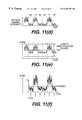
With reference to FIGS. 11(a)-11(f), functional features of the present invention will be compared with those of the circuitry shown in FIG. 7. The optical signal intensity is assumed to be located between Pmin1 and Pmin0 (see FIG. 8).
FIGS. 11(a)-11(c) respectively illustrate the optical signal, preamplifier output, and limiting amplifier output when the optical receiving element is an APD or the combination of an EDFA and PIN diode. As shown schematically in the drawing, noise is superposed over the signals, in correspondence with the signal distribution shown in FIG. 4. Particularly, the noise superposed over the “1” signal is greater than that superposed over the “0” signal.
The reference voltage VTH(LA) of the prior (or, conventional) limiting amplifier is set just intermediate between the average voltage of the “1” signal output and the average voltage of the “0” signal output of the preamplifier. The gain of the prior limiting amplifier is set so that the linear amplification range is several mV at most. Specifically, only a signal in the linear amplification range defined between the two thick curves is linearly amplified, whereas signals outside the region defined by the two thick curves are ignored, so that a constant voltage is output. Therefore, the limiting amplifier output VLA takes the waveform shown in FIG. 11(c), whereby the “0” signal can be correctly decided, but the “1” signal is buried in noise and cannot be decided correctly.
Referring to FIGS. 11(d)-11(f), on the other hand, the reference voltage of the present invention is set at the same level as that of VTH(LA), but the linear amplification range is as wide as several hundred mV, so that the preamplifier output VPRE is linearly amplified by AWL and further by the AGC amplifier, to achieve a signal VAGC having a desired swing. As a result, the output of the AGC amplifier is a faithful reproduction of the input optical signal waveform (that is, the optical signal is converted faithfully to an electric signal without eliminating or altering any data present in the optical signal). If the decision signal VTH(DEC) is set slightly closer to the “0” peak with respect to the VAGC, therefore, it is possible to decide the signal normally.
FIG. 12 illustrates certain circuit elements of FIG. 9 in greater detail. FIG. 12 omits the construction of the optical receiving element, the decision circuit, and the clock-extraction circuit.
The signal current from the optical receiving element is input to a terminal IIN of the preamplifier PRE. The AGC amplifier has a dedicated output terminal VAGC for providing an input to the decision circuit DEC and to the clock-extraction circuit CEXT. Further details of the circuitry shown in FIG. 12 and related embodiments will be discussed next. The optical receiver, however, is not limited to the circuitry shown in FIG. 12 or the related embodiments discussed below, but can take a variety of modes that are exemplified by the disclosed embodiments.
Turning to FIG. 13, an embodiment of an amplifier with a limiting function AWL is discussed. The amplifier AWL includes a differential amplifier constructed of bipolar transistors QA0 and QA1. When the signal input to terminal IN is close to the reference voltage Vref, the amplifier AWL acts as a linear amplifier having a gain A generally expressed by the following formula:
A=RC/((2VT/IA)+RE)  (Formula 2).
In Formula 2, RC is the resistance of the load resistance RC0, RE is the resistance of the emitter resistance REO. VT=q/kT, and IA is the bias current of the differential amplifier, wherein q, k, and T designate the amount of charge of an electron, Boltzmann's constant, and temperature, respectively. The differential amplification circuit shown in FIG. 13 needs to have its left circuit (comprising RC0, QA0, RE0, and CE0) be symmetrical with its right circuit (comprising RC1, QA1, RE1 and CE1), each of which expands from the ground level in the upper part of this figure to the constant current source in the bottom part of this figure. Practically, an error (a difference) of 3% at most can be allowed in a parameter (resistance, capacitance, etc.) of each circuit element between left and right; however, this error is deleted for designing the circuit. Thus, according to the circuit diagram, the resistance of RC1 is set to be equal to RC0 and RC, and the resistance of RE1 is set to be equal to RE0 and RE.
The linear amplification range VLR is generally expressed by the following formula:
VLR=2RE·IA  (Formula 3).
The capacitors CE0 and CE1 are peaking capacitors acting to improve the gain at high frequencies and to widen the bandwidth.
FIG. 14 shows another embodiment of the amplifier AWL. This embodiment is different from that shown in FIG. 13 in that cascode transistors QCS0 and QCS1 are connected with the collectors of transistors QA0 and QA1. The gain and the linear amplification range are expressed as in the embodiment shown in FIG. 13 by Formulas 2 and 3. By connecting the cascode transistors, the Miller capacitance of the transistor QA0 can be reduced, and the bandwidth can be widened more than in the embodiment of FIG. 13.
FIG. 15 shows another embodiment of the amplifier AWL, which uses a transimpedance circuit as the load circuit in place of the resistances RC0 and RC1. Transistors QF0 and QF1, resistances RF0, RF1, RC2, and RC3, and a current source IF constitute the transimpedance circuit, which acts to lower the input impedance as viewed from the collectors of the transistors QA0 and QA1, and to reduce the Miller capacitance. As a result, the bandwidth can be widened more than that of the embodiment shown FIG. 13.
The gain A of the circuit shown in FIG. 15 can be generally expressed by the following formula:
A=RF/((2VT/IA)+RE)  (Formula 4).
In Formula 4, RF is the resistance of the feedback resistance RF0. The differential amplification circuit shown in FIG. 15 needs to have its left and right circuits be symmetrical with each other expanding from the ground level downward to the constant current source in FIG. 13. Thus, although a difference in the resistance between RF0 and RF1 can be 3% at most in practice, RF1 must be set equal to RF0 for designing this circuit. The linear amplification range is expressed by Formula 3.
In each of the embodiments of FIGS. 13-15, the output is extracted directly from the differential amplifier, but the output may be extracted, if necessary, through a buffer circuit, such as an emitter follower.
FIG. 16 shows a preferred embodiment of the preamplifier PRE of the present invention, embodied as a transimpedance amplifier. The transimpedance ZT of the present circuit is substantially equal to RF2. The reason why ZT equals RF2 is explained with reference to the following Formula 5, defining the transimpedance ZT:
Z T=( RF 2 ·A 0)/(1+A 0)  (Formula 5)
In Formula 5, A0 is the gain of the circuit comprising the transistor QP0 and the load resistance RL, and RF2 is the resistance of RF2, shown in FIG. 16. The circuit comprising QP0 and RL is designed to have a large gain A0 so that the following Formula 6 becomes approximately effective:
A 0/(1+A 0)  (Formula 6)
According to Formula 6, it is clear that the transimpedance ZT can be expressed approximately as RF2.
On the other hand, the bandwidth of the preamplifier is dominated by the pole, which is determined by the product of the capacitance of the input unit (i.e., the input capacitance of the preamplifier and the capacitance of the photodiode) Cin and the input resistance of the preamplifier Zin. The pole is denoted by the time constant of τ=Resistance×Capacitance as −2π/τ. Therefore, the pole becomes larger (the time constant becomes smaller), and the preamplifier can respond to the received optical pulses more quickly. In other words, the larger pole enables the preamplifier to receive optical signals transmitted at shorter intervals. The input resistance Zin mentioned above is generally expressed by the following Formula 7:
Zin=RF 2 /AE  (Formula 7).
In Formula 7, AE is the open loop gain of an emitter common amplifier. According to Formula 7, the open loop gain can be retained so large even at high frequencies (setting the Zin smaller) that the bandwidth for receiving the optical signals can be widened.
FIG. 17 shows another embodiment of the preamplifier, using a cascode connection. This embodiment is different from that of FIG. 16 in that the cascode transistor QCS2 is connected with the collector of the transistor QP0. By connecting the cascode transistor in this manner, the Miller capacitance of the transistor QP0 can be reduced, to reduce the input capacitance of the preamplifier. As a result, the bandwidth can be made even wider. However, since the phase margin of the feedback loop is reduced, the flatness of the frequency response must be considered.
In each of FIGS. 16 and 17, the output is made through a one-stage emitter follower, but the emitter follower may have additional stages, if necessary.
FIG. 18 shows an example of an AGC amplifier suited for the optical receiver of the present invention. In this embodiment, a transimpedance circuit is employed as the load circuit, which can be a resistor. For example, the terminal INO in FIG. 18 is connected to one of the terminals of VAWL0 in FIGS. 13, 14 and 15, and the terminal IN1 in FIG. 18 is connected to one of the terminals of VAWL0 in FIGS. 13, 14 and 15, respectively. The gain of the AGC amplifier is increased if the voltage difference between control signals VCNT0 and VCNT1 is enlarged, and decreased if the voltage difference is reduced. A plural-stage cascade amplifier may be employed when the gain is too small with one stage of the present circuit. The control signals VCNT0 and VCNT1 may by controlled by a technique combining a peak detector PD, a reference circuit REF, and a gain controller GC, as disclosed in FIG. 1, for making the setting by detecting the swing of the VAGC and by comparing it with a nominal voltage VN.
Although this embodiment has been described with the output extracted directly from the AGC amplifier, the output may be extracted through a buffer circuit such as an emitter follower.
FIG. 19 shows an embodiment of a reference voltage generator VRG constituted by a low-pass filter constituted by a resistance RLP and a capacitance CLP. Here, this capacitance CLP may be either disposed in a semiconductor chip or connected from the outside. The center voltage of the preamplifier output VPRE can be obtained and output as the reference voltage Vref by extracting the DC component from VPRE using the low-pass filter.
FIG. 20 shows another possible embodiment for the reference voltage generator. The present circuit is composed of a circuit TH for detecting the high voltage of the preamplifier output VPRE(H), a circuit BH for detecting the low voltage VPRE(L), and resistances RA1 and RA2. These resistances are set equal to each other. When VPRE takes a high voltage, the capacitance CTH is charged by the transistor QTH to a voltage of VPRE(H)−VBE, wherein VBE is a bias voltage between the base and emitter of the transistor QTH. When the preamplifier output takes a low voltage, the capacitance CBH is discharged by the diode DBH to a voltage of VPRE(L)+VBE. When these two voltages are divided by the resistances RA1 and RA2, it is possible to generate a voltage just at the center between the high voltage and the low voltage of the preamplifier output VPRE.
FIG. 21 shows another embodiment for the optical receiver shown in FIG. 9. FIG. 21 does not show all of the elements of the FIG. 9 circuit, omitting the optical receiving element, the AGC amplifier, the decision circuit, and the clock-extraction circuit, although these elements are present in the optical receiver. The IIN terminal of the preamplifier PRE is fed with the signal current from the optical receiving element, and the VAWL terminal of the amplifier AWL is electrically connected with the voltage signal input terminal of the AGC amplifier.
As shown in FIG. 21, the optical receiver receives the signal current IIN, which is generated by the optical receiving element in accordance with the input optical signal, which may be transmitted at 10 Gb/s, over a wide dynamic range leading to the swing current value of 2 mA at most. In order to receive an input current signal IIN that has a wide dynamic range with a high transimpedance gain, the optical receiver includes a transimpedance amplification stage constituted by the preamplifier PRE, a present limiting amplification stage constituted by the present limiting amplifier AWL, and a reference voltage generator VRG for feeding the reference voltage Vref to the present limiting amplifier AWL. A bias voltage feeder Vbias feeds the bias voltage to the preamplifier PRE. Each unit is equipped with terminals for receiving supply voltages VCC and VEE (wherein VEE<VCC), and constant current sources (indicated by circled arrows) are provided at transistor emitters as shown.
The reference voltage generator, composed of the low-pass filter having the external capacitor CEXT, outputs the intermediate value of the output swing voltage, as generated by the transimpedance amplification stage, as the reference voltage Vref. One transistor T4 of the differential amplifier in the present limiting amplifier AWL receives the preamplifier output voltage VPRE at its base, and the other transistor T5 receives the reference voltage Vref at its base. As a result, linear amplification is performed at both the transimpedance amplification stage and the present limiting amplification stage for the signal current IIN to establish a high impedance gain if the IIN value is small, but the impedance gain is suppressed to a desired value by the limiting amplification function of the present limiting amplification stage if the IIN value is large.
More specifically, as shown in FIG. 22, the present limiting amplification stage exhibits the linear amplification function for a signal current IIN less than about 400 μA, which is predetermined by the circuitry of the present limiting amplifier AWL, and exhibits the limiting function for a signal current greater than 400 μA irrespective of the value of IIN As a result, in the present limiting amplification stage, a weak signal IIN can be transmitted without fail to the AGC amplifier, and the distortion of the output signal waveform can be suppressed even if the dynamic range of IIN extends from several μA to 2 mA. Consequently, the present limiting amplification stage keeps and improves the signal decision accuracy in the decision circuit DEC.
In FIG. 21, the preamplifier PRE includes an emitter common amplifier having the transistor T1 and the resistance R2, and a shunt feedback loop having the transistor T2, the diode D1, and the resistance R1. The present limiting amplifier AWL has a wide-band differential amplifier and an output buffer. To improve the frequency response characteristics of these two amplifiers, moreover, the bias voltage feeder Vbias is connected with the preamplifier PRE, and the peaking network is connected with the present limiting amplifier AWL.
In the preamplifier PRE, in order to suppress the transimpedance fluctuation for the frequency response to reduce the fluctuation of the eye-diagram, the bias voltage to be applied to the resistance R2 has to be stabilized. The emitter common amplifier of the preamplifier PRE is susceptible to the influences of the current fluctuation of the transistor T1, and determines the frequency response characteristics of the preamplifier. Therefore, the bias voltage must be free from the influences of the fluctuation of VCC so that it may be stabilized. The bias voltage, as shown in FIG. 21, is independent of the fluctuation of VCC because it is determined by the earth voltage and the circuit components.
On the other hand, the present limiting amplifier AWL must be able to respond to a wider frequency range than that of the preamplifier PRE, so that it is connected with the peaking network composed of resistances R3 and R4 and a capacitor CP. A load circuit composed of transistors T6 and T7 and resistances R5 and R6 exhibits a low input impedance by feedback through the resistances R5 and R6, so that the Miller effect of the transistor pair T4 and T5 (the differential input circuit) can be suppressed, and a wide frequency bandwidth of the present limiting amplifier AWL is realized.
For high driving capability and flatness of frequency response, the output buffer of the present limiting amplifier AWL is equipped with a two-stage emitter follower (transistors T8, T10 or T9, T11) and damping resistors R10 and R11. The output signal of the preamplifier is branched by the transistor T12 and input to the reference voltage generator VRG. This reference voltage generator is constructed of a low-pass filter composed of a resistor R14 and capacitors CLP and CEXT, and an emitter follower transistor T13. Its output voltage Vref indicates the intermediate value of the output voltage VPRE of the preamplifier PRE.
Each of the foregoing embodiments employs bipolar transistors, but the optical receiver can be realized in each case with field effect transistors (such as metal-oxide-semiconductor field effect transistors or metal-semiconductor field effect transistors) in place of the bipolar transistors, with appropriate modifications well understood by the person of ordinary skill.
FIG. 23 shows the optical receiver circuit of FIG. 12, substituting MOS (Metal-Oxide-Semiconductor)-type field effect transistors for all of the bipolar transistors thereof.
In the optical receiver of FIG. 12, the transistors QP0, QEF in the preamplification stage, the transistors QA0, QA1 in the present limiting amplification stage, and the transistors QIN(0), QIN(1), QAMP(1), QAMP(2), QAMP(3), QAMP(4), QF0, and QF1 in the AGC amplification stage have NPN-type bipolar transistor structures having collector and emitter regions of N-conduction type and base regions of P-conduction type. In contrast to the optical receiver of FIG. 12, each transistor in FIG. 23 has a MOS-type transistor structure having an N-channel (i.e., an N-channel MOSFET).
An N-channel MOSFET comprises source and drain regions of N-conduction type separated from each other by a semiconductor region of P-conduction type. On the main surface of the semiconductor region of P-type disposed between the source and drain regions, the oxide film (the insulating film) is formed, and furthermore, a gate electrode is formed on the oxide film so as to apply an electric field to the semiconductor region of P-type via the oxide film.
To optimize the signal processing rate for an optical communication system for a trunk line, bipolar transistors are preferable. However, for integrating the optical receiver circuit of the present invention on the same semiconductor substrate, MOSFETs are preferable, because the isolation between the transistors formed monolithically can be fabricated easier than the bipolar transistors.
Each N-channel MOSFET in FIG. 23 sets the potential of its semiconductor region of P-type between its source and drain regions equal to the lower side of the circuitry (the source potential), but the potential condition of the semiconductor region of P-type can be modified and is not limited to the manner of this embodiment.
FIG. 24 shows an optical communication system employing the present optical receiver.
To emphasize the concept of the present optical communication system, the functions of the telephone stations (central offices) designated as TS(A), TS(B), and TS(C) are limited to transmitting the optical signal toward the telephone station TS(R) via optical fiber cables designated as LINE A, LINE B, and LINE C in FIG. 24. In contrast to the telephone stations TS(A), TS(B), TS(C), the functions of the telephone station TS(R) are limited to receiving the optical signals from the telephone stations TS(A), TS(B), TS(C). In practice, the optical signals are transmitted bi-directionally between the telephone stations. In FIG. 24, the symbols of a telephone set and a computer within the circle designated USERS(A), USERS(B), USERS(C), and USERS(R) show the terminals of the subscribers of TS(A), TS(B), TS(C), and TS(R), respectively.
For the illustrated example, the process for transmitting the information from USERS(A), USERS(B), USERS(C) to the USERS(R) using the present optical communication system is explained below. The information from each subscriber of USERS(A), USERS(B), USERS(C) is transformed to an optical signal having its wavelength in the range of 1.3-1.6 μm in each telephone station, and input into one of the optical fiber cables of LINE A, LINE B, and LINE C bound for the telephone station TS(R). Each spectrum of the intensity of the optical signal transmitted from each telephone station of TS(A), TS(B), TS(C) versus time is shown in FIG. 24. Each information transmitted from the telephone stations of TS(A), TS(B), TS(C) is encoded as digital information consisting of “1”-signals Itrs and “0”-signals where there is no optical pulse.
All of the optical signals transmitted from the telephone station TS(A) during the time Ta0 and Ta1, from the telephone station TS(B) during the time Tb0 and Tb1, and from the telephone station TS(C) during the time Tc0 and Tc1 enter the optical fiber optically connected to the photodiode PD in the telephone station TS(R) via the optical coupler CL (for example, a star coupler disposed in the telephone station TS(R)) or on the trunk line bound therefor. Then, the optical signals received from the telephone stations TS(A), TS(B), TS(C) are processed serially along the time schedule provided for each of these telephone stations, and are decoded to the original information as sent by the subscriber thereof. The decoding apparatus is disposed in the telephone station TS(R) or the terminal of the subscriber thereof, as required by the manner of transmission.
In FIG. 24, the distance AR between the telephone stations TS(A) and TS(R) is set as 20 km, the distance BR between the telephone stations TS(B) and TS(R) is set as 100 km, and the distance CR between the telephone stations TS(C) and TS(R) is set as 500 km, respectively. The optical signals received by the photodiode PD in the telephone station (R) are converted to the voltage signals shown in FIG. 25(a) by the preamplifier PRE. The vertical axis of FIG. 25(a) denotes the voltage of the signal VPRE output by the preamplifier PRE. When the voltage swing of VPRE exceeds VDET, the waveform of the signal deteriorates in the AGC amplifier disposed downstream of the preamplifier PRE, and the error rate for discriminating the signals exceeds the level allowed for practical use. Since the optical signal transmitted from the telephone station TS(A) near the station TS(R) during the time Ta0 and Ta1 is not affected by the optical loss during its propagation through the optical fiber cable LINE A, therefore, it tends to be converted to a strong voltage pulse having its voltage swing Va exceeding VDET by the preamplifier.
In the present optical communication system, the amplifier with limiting function is disposed between the preamplifier PRE and the AGC amplifier AGC, and is designed to limit its output voltage VAWL to the voltage swing of the first voltage V1 (set at a value less then VDET) when the voltage swing of VPRE becomes equal to or larger than V1. Consequently, the digitized information from the telephone station TS(A) can be converted to VAGC without any deterioration of its waveform, and transmitted to the decision circuit DEC.
The threshold voltage VTH(DEC) of the decision circuit is predetermined to the voltage between the voltage V1 and the voltage of zero-level artificially (by the operator, etc.) in the telephone station TS(R). An example voltage of VTH(DEC) is half of V1. The AGC amplifier controls its gain with respect to the voltage swing of the signal input thereto, and gives the signal a sufficient voltage swing exceeding VTH(DEC) for the signal discrimination in the decision circuit. In practical use, the AGC amplifier tunes its gain with respect to the voltage swing of a dummy optical signal transmitted from each of the stations TS(A), TS(B), and TS(C) before transmission of the optical signal of the information to be sent. But such a function of the AGC amplifier is not complete because the AGC amplifier cannot give a sufficient voltage swing to an input signal having a voltage swing below the second voltage V2.
Since the optical signal transmitted from a telephone station TS(C) situated as far as 500 km from the station TS(R) during the time Tc0 and Tc1 is fairly affected by optical loss during its propagation through the optical fiber cable LINE C, therefore, the voltage swing of the signal VPRE to which the optical signal is converted by the preamplifier cannot reach V2 as shown in FIG. 25(a). To discrimination such a weak signal VPRE transmitted from the station TS(A), the decision circuit DEC must be designed to vary its threshold voltage of VTH(DEC) with respect to the voltage swing of the signal VPRE. However, this method cannot be applied to discriminate a signal consisting of pulses transmitted at such short intervals as 1 ns or less.
In the present optical communication system, the amplifier with limiting function mentioned above linearly amplifies the signal VPRE having a voltage swing of Vc, and converts it to the signal VAWL having a larger voltage swing than V2 as shown in FIG. 25(b). Although the voltage swing of the signal amplified by the amplifier with limiting function does not reach the threshold voltage of VTH(DEC), it can be discriminated in the decision circuit by an additional linear amplification by an AGC amplifier and conversion to the signal of VAGC as shown in FIG. 25(c).
As mentioned above, the present optical communication system inserts a linear amplifier between the preamplifier and the AGC amplifier, which assists the AGC amplifier and limits its linear amplification with respect to a voltage swing of the signal input thereto. Thus, in the present optical communication system, the signal transmitted from the preamplifier to the AGC amplifier can be processed, whether it is to be limited to the predetermined voltage or amplified linearly according to its swing voltage during its steady transmission. Processing the signal under its steady transmission form the preamplifier to the AGC amplifier enables the optical receiver to widen its dynamic range of optical signal intensity, to be received without any limitation of its transmission rate that might be caused by the prior art as tuning the gain of the preamplifier or the threshold voltage of the decision circuit.
Various modifications of the present invention will become apparent to those of ordinary skill in the art. All such modifications that basically rely upon the teachings through which the invention has advanced the state of the art are probably considered within the spirit and scope of the invention.

Claims (6)

We claim:
1. An optical receiver for converting an optical signal received into an electrical signal to output the electric signal, comprising:
a photoelectric converter having an electric current signal output;
a preamplifier connected to receive the current signal output by the photoelectric converter, and having a voltage signal output;
an amplifier having a limiting function and connected to receive the voltage signal output by the preamplifier, to linearly amplify the voltage signal when the voltage signal is different from a reference voltage by less than or equal to a predetermined voltage, and to limitedly amplify said voltage signal when the voltage signal is different from the reference voltage by more than the predetermined voltage; and
an automatic-gain-control amplifier connected to receive and amplify the output voltage signal of said amplifier having the limiting function, to output a signal having a constant swing,
wherein the output signal swing of said amplifier having the limiting function satisfies the following relation within a desired dynamic range of said optical signal:
ΔVAWL<Rs·Δt,
wherein ΔVAWL is the output signal swing of said amplifier having the limiting function; Δt is the time period to be occupied by a single optical bit; and Rs is the slew rate of said amplifier having the limiting function.
2. An optical receiver according to claim 1, wherein said photoelectric converter is an avalanche photodiode.
3. An optical receiver according to claim 1, wherein said photoelectric converter includes an optical fiber amplifier and a PIN photodiode.
4. An optical receiver according to claim 1, wherein the predetermined voltage is set larger than the difference between the voltage signal output by said preamplifier and said reference voltage at the minimum receiver sensitivity.
5. An optical receiver according to claim 4, wherein said photoelectric converter is an avalanche photodiode.
6. An optical receiver according to claim 4, wherein said photoelectric converter includes an optical fiber amplifier and a PIN photodiode.
US09/041,973 1997-03-13 1998-03-13 Optical receiver Expired - Fee Related US6304357B1 (en)

Priority Applications (1)

Application Number Priority Date Filing Date Title
US09/946,450 US6658217B2 (en) 1997-03-13 2001-09-06 Optical receiver

Applications Claiming Priority (2)

Application Number Priority Date Filing Date Title
JP9-058790 1997-03-13
JP5879097 1997-03-13

Related Child Applications (1)

Application Number Title Priority Date Filing Date
US09/946,450 Continuation US6658217B2 (en) 1997-03-13 2001-09-06 Optical receiver

Publications (1)

Publication Number Publication Date
US6304357B1 true US6304357B1 (en) 2001-10-16

Family

ID=13094376

Family Applications (2)

Application Number Title Priority Date Filing Date
US09/041,973 Expired - Fee Related US6304357B1 (en) 1997-03-13 1998-03-13 Optical receiver
US09/946,450 Expired - Fee Related US6658217B2 (en) 1997-03-13 2001-09-06 Optical receiver

Family Applications After (1)

Application Number Title Priority Date Filing Date
US09/946,450 Expired - Fee Related US6658217B2 (en) 1997-03-13 2001-09-06 Optical receiver

Country Status (1)

Country Link
US (2) US6304357B1 (en)

Cited By (24)

* Cited by examiner, † Cited by third party
Publication number Priority date Publication date Assignee Title
US20020063917A1 (en) * 2000-06-27 2002-05-30 Nec Corporation Optical data bus communication in an artificial satellite
US6433899B1 (en) * 1998-10-06 2002-08-13 Nortel Networks Limited Eye quality monitor for a 2R regenerator
US20020135845A1 (en) * 2001-03-26 2002-09-26 Robinson Michael A. Fiber optic receiver with an adjustable bandwidth post-amplifier
WO2002080481A1 (en) * 2001-04-02 2002-10-10 Adc Telecommunications, Inc. Increased transmission capacity for a fiber-optic link
US6504140B1 (en) * 1999-08-27 2003-01-07 Hitachi, Ltd. Optical interconnection receiving module
US20030011845A1 (en) * 2000-04-11 2003-01-16 Gilles Billet Wavelength multiplexing optical fibre transmission device
US20030122057A1 (en) * 2001-12-27 2003-07-03 Jin-Soo Han Optical signal receiving apparatus and method using the same
US6608710B1 (en) * 2000-01-31 2003-08-19 Leitch Technology International Inc. Automatic gain control circuit and optical receiver
US6674974B1 (en) 2000-07-28 2004-01-06 Terabeam Corporation Method and apparatus for tracking in an optical communications system
US20040057725A1 (en) * 2002-09-23 2004-03-25 Jyung-Chan Lee Method and apparatus for optimizing decision level of signal output from optical receiver
US20040070805A1 (en) * 2002-06-04 2004-04-15 Eiselt Michael H. Apparatus and method for optimum decision threshold setting
US6768876B1 (en) * 2000-07-28 2004-07-27 Terabeam Corporation Method and apparatus for tracking an optical communications system
US20040208645A1 (en) * 2002-05-31 2004-10-21 Buckman Lisa A. Method and apparatus for optical transmission of wavelength-encoded modulation formats
US20050135818A1 (en) * 2003-12-18 2005-06-23 Lee Jyung C. Apparatus for controlling decision threshold voltage to optical receiver
US6915083B1 (en) * 1998-12-15 2005-07-05 Zilog, Inc. Signal receiver having wide band amplification capability
US6917233B1 (en) * 2002-09-11 2005-07-12 Koninklijke Philips Electronics N.V. Limiting amplifier and method for amplifying an input signal
US6980747B1 (en) * 2000-11-28 2005-12-27 Harris Corporation Optically amplified receiver
US20060022750A1 (en) * 2004-07-28 2006-02-02 Industrial Technology Research Institute High frequency amplifier
WO2007014299A2 (en) * 2005-07-25 2007-02-01 Mrv Communications, Inc. Automatic gain control
US20080107424A1 (en) * 2002-07-22 2008-05-08 Broadcom Corporation Bit Stream Conditioning Circuit having Adjustable Input Sensitivity
US20080129378A1 (en) * 2006-12-05 2008-06-05 Sung Kyung Park Detector for automatic gain control
KR100866091B1 (en) * 2007-02-28 2008-10-31 고려대학교 산학협력단 Optical receiver with threshold convergence, Audio apparatus and Communication apparatus using this
TWI650963B (en) * 2014-06-19 2019-02-11 日商瑞薩電子股份有限公司 Optical receiver
EP3917037A1 (en) * 2020-05-27 2021-12-01 Molex, LLC Optical receiving device

Families Citing this family (15)

* Cited by examiner, † Cited by third party
Publication number Priority date Publication date Assignee Title
EP1357682A1 (en) * 2002-04-23 2003-10-29 Agilent Technologies, Inc. - a Delaware corporation - Module apparatus for optical communication and circuit pack therefor
US6784749B1 (en) * 2003-02-24 2004-08-31 Intel Corporation Limiting amplifier with active inductor
WO2005022784A1 (en) * 2003-08-29 2005-03-10 Koninklijke Philips Electronics N.V. Optical receiver
US7123098B2 (en) * 2004-03-15 2006-10-17 Intel Corporation Transimpedance amplifier with differential peak detector
US7349017B2 (en) * 2004-04-21 2008-03-25 Avago Technologies Ecbu Ip Pte Ltd Color sensor circuit with integrated programmable gain selection
KR100674087B1 (en) * 2004-11-22 2007-01-24 한국전자통신연구원 Clock signal generation apparatus and method using asymmetrical distortion of NRZ signal, and optical transmission and receiving system using its
US8064771B2 (en) * 2005-06-30 2011-11-22 Infinera Corporation Active control loop for power control of optical channel groups
US7388436B2 (en) * 2005-11-02 2008-06-17 Marvell World Trade Ltd High-bandwidth high-gain amplifier
US7397306B2 (en) * 2005-11-02 2008-07-08 Marvell World Trade Ltd. High-bandwidth high-gain amplifier
JP2009017265A (en) * 2007-07-05 2009-01-22 Eudyna Devices Inc Electronic circuit
US8744268B2 (en) 2008-03-10 2014-06-03 Emcore Corporation Passive optical network module
US8145060B2 (en) * 2008-05-09 2012-03-27 Emcore Corporation Passive optical network transceiver with temperature compensation circuit
US20100150561A1 (en) * 2008-12-12 2010-06-17 Seung-Hyun Cho Optical receiver, optical line terminal and method of recovering received signals
US10958230B2 (en) * 2018-09-10 2021-03-23 Elenion Technologies, Llc Reconfigurable optical receivers with extended dynamic range
US11218120B2 (en) * 2019-05-22 2022-01-04 Integrated Device Technology, Inc. Programmable amplifiers

Citations (14)

* Cited by examiner, † Cited by third party
Publication number Priority date Publication date Assignee Title
US4665560A (en) * 1985-05-20 1987-05-12 Texas Instruments Incorporated Wide band automatic gain control with limiting amplifiers
JPH0567930A (en) 1991-09-09 1993-03-19 Nec Eng Ltd Voltage amplifier circuit
JPH05218758A (en) 1992-02-07 1993-08-27 Japan Aviation Electron Ind Ltd Optical signal receiver
JPH05259752A (en) 1992-03-16 1993-10-08 Fujitsu Ltd Optical receiver
JPH0738342A (en) 1993-07-23 1995-02-07 Fujitsu Ltd Pre-amplifier
JPH07193437A (en) 1993-12-27 1995-07-28 Hitachi Ltd Gain switching optical receiver amplifier circuit
JPH08139526A (en) 1994-11-07 1996-05-31 Mitsubishi Electric Corp Optical reception equipment
US5636048A (en) * 1994-03-17 1997-06-03 Fujitsu Limited Equalizing amplifier, receiver using the same and preamplifier
JPH09246879A (en) 1996-03-14 1997-09-19 Fujitsu Ltd Preamplifier circuit
US5859718A (en) * 1994-12-28 1999-01-12 Canon Kabushiki Kaisha Simplified switching control device, and a network system for employing the device: and a simplified switching control method, and a communication method for employing the method
US5917639A (en) * 1995-05-01 1999-06-29 Nec Corporation Optical receiver
US6018554A (en) * 1996-05-17 2000-01-25 Texas Instruments Incorporated Automatic gain control circuit and method for full gain restart
US6031219A (en) * 1997-01-07 2000-02-29 Nec Corporation Bias voltage supply circuit for photoelectric converting element and photodetection circuit
US6191879B1 (en) * 1997-07-23 2001-02-20 Nec Corporation Offset control for burst-mode optical receiver

Family Cites Families (1)

* Cited by examiner, † Cited by third party
Publication number Priority date Publication date Assignee Title
JPS60501286A (en) * 1983-05-12 1985-08-08 アメリカン テレフオン アンド テレグラフ カムパニ− communication network

Patent Citations (14)

* Cited by examiner, † Cited by third party
Publication number Priority date Publication date Assignee Title
US4665560A (en) * 1985-05-20 1987-05-12 Texas Instruments Incorporated Wide band automatic gain control with limiting amplifiers
JPH0567930A (en) 1991-09-09 1993-03-19 Nec Eng Ltd Voltage amplifier circuit
JPH05218758A (en) 1992-02-07 1993-08-27 Japan Aviation Electron Ind Ltd Optical signal receiver
JPH05259752A (en) 1992-03-16 1993-10-08 Fujitsu Ltd Optical receiver
JPH0738342A (en) 1993-07-23 1995-02-07 Fujitsu Ltd Pre-amplifier
JPH07193437A (en) 1993-12-27 1995-07-28 Hitachi Ltd Gain switching optical receiver amplifier circuit
US5636048A (en) * 1994-03-17 1997-06-03 Fujitsu Limited Equalizing amplifier, receiver using the same and preamplifier
JPH08139526A (en) 1994-11-07 1996-05-31 Mitsubishi Electric Corp Optical reception equipment
US5859718A (en) * 1994-12-28 1999-01-12 Canon Kabushiki Kaisha Simplified switching control device, and a network system for employing the device: and a simplified switching control method, and a communication method for employing the method
US5917639A (en) * 1995-05-01 1999-06-29 Nec Corporation Optical receiver
JPH09246879A (en) 1996-03-14 1997-09-19 Fujitsu Ltd Preamplifier circuit
US6018554A (en) * 1996-05-17 2000-01-25 Texas Instruments Incorporated Automatic gain control circuit and method for full gain restart
US6031219A (en) * 1997-01-07 2000-02-29 Nec Corporation Bias voltage supply circuit for photoelectric converting element and photodetection circuit
US6191879B1 (en) * 1997-07-23 2001-02-20 Nec Corporation Offset control for burst-mode optical receiver

Non-Patent Citations (2)

* Cited by examiner, † Cited by third party
Title
M. Moller et al, "13 Gb/s si-Bipolar AGC Amplifier IC with High Gain and Wide Dynamic Range for Optical-Fiber Receivers", IEEE Journal of Solid-State Circuits, vol. 29, No. 7, Jul. 1994, p. 815-821.
M. Nakamura et al, "An Instantaneous Response CMOS Optical Receiver IC with Wide Dynamic Range and Extremely High Sensitivity Using Feed-Forward Auto-Bias Adjustment", IEEE Journal of Solid-State Circuits, vol. 30, No. 9, Sept. 1995, p. 991-997.

Cited By (42)

* Cited by examiner, † Cited by third party
Publication number Priority date Publication date Assignee Title
US6433899B1 (en) * 1998-10-06 2002-08-13 Nortel Networks Limited Eye quality monitor for a 2R regenerator
US7212749B2 (en) 1998-12-15 2007-05-01 Zilog, Inc. Signal receiver having wide band amplification capability
US6915083B1 (en) * 1998-12-15 2005-07-05 Zilog, Inc. Signal receiver having wide band amplification capability
US20050158053A1 (en) * 1998-12-15 2005-07-21 Hamilton T. A. Signal receiver having wide band amplification capability
US6504140B1 (en) * 1999-08-27 2003-01-07 Hitachi, Ltd. Optical interconnection receiving module
US6608710B1 (en) * 2000-01-31 2003-08-19 Leitch Technology International Inc. Automatic gain control circuit and optical receiver
US20030011845A1 (en) * 2000-04-11 2003-01-16 Gilles Billet Wavelength multiplexing optical fibre transmission device
US20020063917A1 (en) * 2000-06-27 2002-05-30 Nec Corporation Optical data bus communication in an artificial satellite
US6768876B1 (en) * 2000-07-28 2004-07-27 Terabeam Corporation Method and apparatus for tracking an optical communications system
US6674974B1 (en) 2000-07-28 2004-01-06 Terabeam Corporation Method and apparatus for tracking in an optical communications system
US6980747B1 (en) * 2000-11-28 2005-12-27 Harris Corporation Optically amplified receiver
US7072590B2 (en) * 2001-03-26 2006-07-04 Avago Technologies General Ip Pte. Ltd. Fiber optic receiver with an adjustable bandwidth post-amplifier
US20020135845A1 (en) * 2001-03-26 2002-09-26 Robinson Michael A. Fiber optic receiver with an adjustable bandwidth post-amplifier
US20050147418A1 (en) * 2001-04-02 2005-07-07 Adc Telecommunications, Inc. Increased transmission capacity for a fiber-optic link
US6643471B2 (en) * 2001-04-02 2003-11-04 Adc Telecommunications, Inc. Increased transmission capacity for a fiber-optic link
US6963697B2 (en) 2001-04-02 2005-11-08 Adc Telecommunications, Inc. Increased transmission capacity for a fiber-optic link
WO2002080481A1 (en) * 2001-04-02 2002-10-10 Adc Telecommunications, Inc. Increased transmission capacity for a fiber-optic link
US6822214B2 (en) * 2001-12-27 2004-11-23 Electronics And Telecommunications Research Institute Optical signal receiving apparatus and method using the same
US20030122057A1 (en) * 2001-12-27 2003-07-03 Jin-Soo Han Optical signal receiving apparatus and method using the same
US20040208645A1 (en) * 2002-05-31 2004-10-21 Buckman Lisa A. Method and apparatus for optical transmission of wavelength-encoded modulation formats
US7092641B2 (en) * 2002-05-31 2006-08-15 Avago Technologies Fiber Ip (Singapore) Pte. Ltd. Method and apparatus for optical transmission of wavelength-encoded modulation formats
US7603042B2 (en) * 2002-06-04 2009-10-13 Eiselt Michael H Apparatus and method for optimum decision threshold setting
US20040070805A1 (en) * 2002-06-04 2004-04-15 Eiselt Michael H. Apparatus and method for optimum decision threshold setting
US8014471B2 (en) * 2002-07-22 2011-09-06 Broadcom Corporation Bit stream conditioning circuit having adjustable input sensitivity
US20080107424A1 (en) * 2002-07-22 2008-05-08 Broadcom Corporation Bit Stream Conditioning Circuit having Adjustable Input Sensitivity
US6917233B1 (en) * 2002-09-11 2005-07-12 Koninklijke Philips Electronics N.V. Limiting amplifier and method for amplifying an input signal
US20040057725A1 (en) * 2002-09-23 2004-03-25 Jyung-Chan Lee Method and apparatus for optimizing decision level of signal output from optical receiver
KR100467323B1 (en) * 2002-09-23 2005-01-24 한국전자통신연구원 Optimization method and apparatus of decision level of output signal in optical receiver
US7298978B2 (en) * 2002-09-23 2007-11-20 Electronics And Telecommunications Research Institute Method and apparatus for optimizing decision level of signal output from optical receiver
US7313333B2 (en) * 2003-12-18 2007-12-25 Electronics And Telecommunications Research Institute Apparatus for controlling decision threshold voltage to optical receiver
US20050135818A1 (en) * 2003-12-18 2005-06-23 Lee Jyung C. Apparatus for controlling decision threshold voltage to optical receiver
US20060022750A1 (en) * 2004-07-28 2006-02-02 Industrial Technology Research Institute High frequency amplifier
US7157976B2 (en) 2004-07-28 2007-01-02 Industrial Technology Research Institute High frequency amplifier
WO2007014299A3 (en) * 2005-07-25 2007-12-13 Mrv Communications Inc Automatic gain control
WO2007014299A2 (en) * 2005-07-25 2007-02-01 Mrv Communications, Inc. Automatic gain control
US20070071455A1 (en) * 2005-07-25 2007-03-29 Near Margalit Automatic gain control
US20080129378A1 (en) * 2006-12-05 2008-06-05 Sung Kyung Park Detector for automatic gain control
US7466196B2 (en) * 2006-12-05 2008-12-16 Electronics And Telecommunications Research Institute Detector for automatic gain control
KR100866091B1 (en) * 2007-02-28 2008-10-31 고려대학교 산학협력단 Optical receiver with threshold convergence, Audio apparatus and Communication apparatus using this
TWI650963B (en) * 2014-06-19 2019-02-11 日商瑞薩電子股份有限公司 Optical receiver
EP3917037A1 (en) * 2020-05-27 2021-12-01 Molex, LLC Optical receiving device
US11411655B2 (en) 2020-05-27 2022-08-09 Molex, Llc Optical receiving device

Also Published As

Publication number Publication date
US6658217B2 (en) 2003-12-02
US20020005974A1 (en) 2002-01-17

Similar Documents

Publication Publication Date Title
US6304357B1 (en) Optical receiver
US6583671B2 (en) Stable AGC transimpedance amplifier with expanded dynamic range
US5844445A (en) Feedback type pre-amplifier
US6072366A (en) Receiver capable of outputting a high quality signal without regard to an input signal level
JPH05304422A (en) Preamplifier for optical communication
US6847263B2 (en) Optical receiver with wide dynamic range transimpedance amplifier
US5146079A (en) Broadband optical receiver with active bias feedback circuit
JPH06177664A (en) Digital photoreception circuit, trans-impedance amplifier circuit and preamplifier circuit
US8248165B2 (en) Amplifier and optical module performing gain control
JP2008211702A (en) Pre-amplifier and optical receiving device using the same
JPS59216339A (en) Light receiver and light transmission system
JP2009010741A (en) Preamplifier, and optical receiver
EP1355464A2 (en) DC removal in an optical receiver
US8144813B2 (en) Receiving method and receiving circuit
US6876260B2 (en) Elevated front-end transimpedance amplifier
CN113300675B (en) Burst mode optical receiver transimpedance amplifier circuit with reduced settling time
JP4072232B2 (en) Optical receiver circuit
KR100381410B1 (en) Burst mode type optical receiver by using multi-stage feedback
US20060078269A1 (en) Video optical receiver
US6785477B1 (en) Optical receiver using variable negative-capacitance circuit
US6844784B1 (en) Wide dynamic range transimpedance amplifier
US20050140396A1 (en) Detecting peak signals
JP3532633B2 (en) Optical receiver
JP3415986B2 (en) Optical receiver amplifier
EP1359673A1 (en) Radio frequency tuner front end with adaptive supply current

Legal Events

Date Code Title Description
AS Assignment

Owner name: HITACHI, LTD., JAPAN

Free format text: ASSIGNMENT OF ASSIGNORS INTEREST;ASSIGNORS:OHHATA, KENICHI;TAKEYARI, RYOJI;MASUDA, TORU;AND OTHERS;REEL/FRAME:011998/0132

Effective date: 19980618

Owner name: HITACHI DEVICE ENGINEERING CO., LTD., JAPAN

Free format text: ASSIGNMENT OF ASSIGNORS INTEREST;ASSIGNORS:OHHATA, KENICHI;TAKEYARI, RYOJI;MASUDA, TORU;AND OTHERS;REEL/FRAME:011998/0132

Effective date: 19980618

FEPP Fee payment procedure

Free format text: PAYOR NUMBER ASSIGNED (ORIGINAL EVENT CODE: ASPN); ENTITY STATUS OF PATENT OWNER: LARGE ENTITY

FPAY Fee payment

Year of fee payment: 4

FPAY Fee payment

Year of fee payment: 8

FEPP Fee payment procedure

Free format text: PAYER NUMBER DE-ASSIGNED (ORIGINAL EVENT CODE: RMPN); ENTITY STATUS OF PATENT OWNER: LARGE ENTITY

FEPP Fee payment procedure

Free format text: PAYOR NUMBER ASSIGNED (ORIGINAL EVENT CODE: ASPN); ENTITY STATUS OF PATENT OWNER: LARGE ENTITY

REMI Maintenance fee reminder mailed
LAPS Lapse for failure to pay maintenance fees
STCH Information on status: patent discontinuation

Free format text: PATENT EXPIRED DUE TO NONPAYMENT OF MAINTENANCE FEES UNDER 37 CFR 1.362

FP Lapsed due to failure to pay maintenance fee

Effective date: 20131016