US6303872B1 - Anti-tombstoning solder joints - Google Patents
Anti-tombstoning solder joints Download PDFInfo
- Publication number
- US6303872B1 US6303872B1 US08/882,482 US88248297A US6303872B1 US 6303872 B1 US6303872 B1 US 6303872B1 US 88248297 A US88248297 A US 88248297A US 6303872 B1 US6303872 B1 US 6303872B1
- Authority
- US
- United States
- Prior art keywords
- electronic circuit
- circuit assembly
- assembly according
- solder joint
- mounting pad
- Prior art date
- Legal status (The legal status is an assumption and is not a legal conclusion. Google has not performed a legal analysis and makes no representation as to the accuracy of the status listed.)
- Expired - Fee Related
Links
Images


Classifications
-
- H—ELECTRICITY
- H05—ELECTRIC TECHNIQUES NOT OTHERWISE PROVIDED FOR
- H05K—PRINTED CIRCUITS; CASINGS OR CONSTRUCTIONAL DETAILS OF ELECTRIC APPARATUS; MANUFACTURE OF ASSEMBLAGES OF ELECTRICAL COMPONENTS
- H05K3/00—Apparatus or processes for manufacturing printed circuits
- H05K3/30—Assembling printed circuits with electric components, e.g. with resistor
- H05K3/32—Assembling printed circuits with electric components, e.g. with resistor electrically connecting electric components or wires to printed circuits
- H05K3/34—Assembling printed circuits with electric components, e.g. with resistor electrically connecting electric components or wires to printed circuits by soldering
- H05K3/341—Surface mounted components
- H05K3/3431—Leadless components
- H05K3/3442—Leadless components having edge contacts, e.g. leadless chip capacitors, chip carriers
-
- H—ELECTRICITY
- H01—ELECTRIC ELEMENTS
- H01L—SEMICONDUCTOR DEVICES NOT COVERED BY CLASS H10
- H01L2224/00—Indexing scheme for arrangements for connecting or disconnecting semiconductor or solid-state bodies and methods related thereto as covered by H01L24/00
- H01L2224/01—Means for bonding being attached to, or being formed on, the surface to be connected, e.g. chip-to-package, die-attach, "first-level" interconnects; Manufacturing methods related thereto
- H01L2224/02—Bonding areas; Manufacturing methods related thereto
- H01L2224/04—Structure, shape, material or disposition of the bonding areas prior to the connecting process
- H01L2224/0401—Bonding areas specifically adapted for bump connectors, e.g. under bump metallisation [UBM]
-
- H—ELECTRICITY
- H01—ELECTRIC ELEMENTS
- H01L—SEMICONDUCTOR DEVICES NOT COVERED BY CLASS H10
- H01L2224/00—Indexing scheme for arrangements for connecting or disconnecting semiconductor or solid-state bodies and methods related thereto as covered by H01L24/00
- H01L2224/01—Means for bonding being attached to, or being formed on, the surface to be connected, e.g. chip-to-package, die-attach, "first-level" interconnects; Manufacturing methods related thereto
- H01L2224/02—Bonding areas; Manufacturing methods related thereto
- H01L2224/04—Structure, shape, material or disposition of the bonding areas prior to the connecting process
- H01L2224/04026—Bonding areas specifically adapted for layer connectors
-
- H—ELECTRICITY
- H01—ELECTRIC ELEMENTS
- H01L—SEMICONDUCTOR DEVICES NOT COVERED BY CLASS H10
- H01L2224/00—Indexing scheme for arrangements for connecting or disconnecting semiconductor or solid-state bodies and methods related thereto as covered by H01L24/00
- H01L2224/01—Means for bonding being attached to, or being formed on, the surface to be connected, e.g. chip-to-package, die-attach, "first-level" interconnects; Manufacturing methods related thereto
- H01L2224/10—Bump connectors; Manufacturing methods related thereto
- H01L2224/15—Structure, shape, material or disposition of the bump connectors after the connecting process
- H01L2224/16—Structure, shape, material or disposition of the bump connectors after the connecting process of an individual bump connector
- H01L2224/161—Disposition
- H01L2224/16104—Disposition relative to the bonding area, e.g. bond pad
- H01L2224/16105—Disposition relative to the bonding area, e.g. bond pad the bump connector connecting bonding areas being not aligned with respect to each other
-
- H—ELECTRICITY
- H01—ELECTRIC ELEMENTS
- H01L—SEMICONDUCTOR DEVICES NOT COVERED BY CLASS H10
- H01L2224/00—Indexing scheme for arrangements for connecting or disconnecting semiconductor or solid-state bodies and methods related thereto as covered by H01L24/00
- H01L2224/01—Means for bonding being attached to, or being formed on, the surface to be connected, e.g. chip-to-package, die-attach, "first-level" interconnects; Manufacturing methods related thereto
- H01L2224/10—Bump connectors; Manufacturing methods related thereto
- H01L2224/15—Structure, shape, material or disposition of the bump connectors after the connecting process
- H01L2224/16—Structure, shape, material or disposition of the bump connectors after the connecting process of an individual bump connector
- H01L2224/161—Disposition
- H01L2224/16151—Disposition the bump connector connecting between a semiconductor or solid-state body and an item not being a semiconductor or solid-state body, e.g. chip-to-substrate, chip-to-passive
- H01L2224/16221—Disposition the bump connector connecting between a semiconductor or solid-state body and an item not being a semiconductor or solid-state body, e.g. chip-to-substrate, chip-to-passive the body and the item being stacked
- H01L2224/16225—Disposition the bump connector connecting between a semiconductor or solid-state body and an item not being a semiconductor or solid-state body, e.g. chip-to-substrate, chip-to-passive the body and the item being stacked the item being non-metallic, e.g. insulating substrate with or without metallisation
- H01L2224/16238—Disposition the bump connector connecting between a semiconductor or solid-state body and an item not being a semiconductor or solid-state body, e.g. chip-to-substrate, chip-to-passive the body and the item being stacked the item being non-metallic, e.g. insulating substrate with or without metallisation the bump connector connecting to a bonding area protruding from the surface of the item
-
- H—ELECTRICITY
- H01—ELECTRIC ELEMENTS
- H01L—SEMICONDUCTOR DEVICES NOT COVERED BY CLASS H10
- H01L2924/00—Indexing scheme for arrangements or methods for connecting or disconnecting semiconductor or solid-state bodies as covered by H01L24/00
- H01L2924/30—Technical effects
- H01L2924/38—Effects and problems related to the device integration
- H01L2924/384—Bump effects
-
- H—ELECTRICITY
- H05—ELECTRIC TECHNIQUES NOT OTHERWISE PROVIDED FOR
- H05K—PRINTED CIRCUITS; CASINGS OR CONSTRUCTIONAL DETAILS OF ELECTRIC APPARATUS; MANUFACTURE OF ASSEMBLAGES OF ELECTRICAL COMPONENTS
- H05K2201/00—Indexing scheme relating to printed circuits covered by H05K1/00
- H05K2201/10—Details of components or other objects attached to or integrated in a printed circuit board
- H05K2201/10613—Details of electrical connections of non-printed components, e.g. special leads
- H05K2201/10621—Components characterised by their electrical contacts
- H05K2201/10636—Leadless chip, e.g. chip capacitor or resistor
-
- H—ELECTRICITY
- H05—ELECTRIC TECHNIQUES NOT OTHERWISE PROVIDED FOR
- H05K—PRINTED CIRCUITS; CASINGS OR CONSTRUCTIONAL DETAILS OF ELECTRIC APPARATUS; MANUFACTURE OF ASSEMBLAGES OF ELECTRICAL COMPONENTS
- H05K2203/00—Indexing scheme relating to apparatus or processes for manufacturing printed circuits covered by H05K3/00
- H05K2203/04—Soldering or other types of metallurgic bonding
- H05K2203/0465—Shape of solder, e.g. differing from spherical shape, different shapes due to different solder pads
-
- Y—GENERAL TAGGING OF NEW TECHNOLOGICAL DEVELOPMENTS; GENERAL TAGGING OF CROSS-SECTIONAL TECHNOLOGIES SPANNING OVER SEVERAL SECTIONS OF THE IPC; TECHNICAL SUBJECTS COVERED BY FORMER USPC CROSS-REFERENCE ART COLLECTIONS [XRACs] AND DIGESTS
- Y02—TECHNOLOGIES OR APPLICATIONS FOR MITIGATION OR ADAPTATION AGAINST CLIMATE CHANGE
- Y02P—CLIMATE CHANGE MITIGATION TECHNOLOGIES IN THE PRODUCTION OR PROCESSING OF GOODS
- Y02P70/00—Climate change mitigation technologies in the production process for final industrial or consumer products
- Y02P70/50—Manufacturing or production processes characterised by the final manufactured product
Definitions
- the present invention relates generally to electronic circuit assemblies. More particularly, the present invention relates to electronic circuit assemblies having surface mount devices with anti-tombstoning solder joints.
- a typical surface mount device is mechanically and electrically attached to a printed circuit board (PCB) substrate by providing mounting pads on the substrate, depositing solder paste onto these pads, placing the SMD on the solder paste/mounting pads such that its terminations are aligned with their respective mounting pads, reflowing the solder through the application of heat, and allowing the solder to cool so as to form a solder joint connecting each termination with its respective mounting pad.
- PCB printed circuit board
- Tombstoning occurs when a net moment is exerted on the SMD by melted solder joints at one end of the device such that the device rotates—first about the device's center of mass, and then about a fulcrum point G, located at the outer edge of the bottom termination adjacent the molten solder joint, when the fulcrum point touches down upon the top surface of the adjacent mounting pad—whereupon the SMD “stands up” on that end.
- This causes the device to detach from the unmelted or partially melted solder paste at the opposite end.
- Decentering occurs when a net force is exerted on the device in a direction toward the molten solder joint, thus tending to pull the opposite end of the device off of its unmelted or partially melted solder paste.
- the present invention overcomes the disadvantages of the prior art by providing an electronic circuit assembly having anti-tombstoning solder joints comprising: a substrate having at least one mounting pad thereon; an SMD having at least one termination; and at least one solder joint connecting each termination to its respective mounting pad.
- Each solder joint is convex in shape, having a continuous and substantially circular arcuate outer profile and covering substantially all of the mounting pad and substantially all of a top portion of each termination.
- Each mounting pad has a predetermined length and each solder joint has a predetermined volume of solder selected such that a positive net anti-tombstoning moment is exerted upon the SMD when at least one solder joint is in a molten state.
- the present invention reduces tombstoning while providing flexibility in the spacing apart of mounting pads located at opposing ends of the SMD.
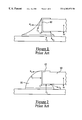
- FIG. 1 is an elevational view of a concave prior art solder joint subjected to tombstoning forces.
- FIG. 2 is an elevational view of a convex prior art solder joint subjected to tombstoning forces.
- FIG. 3 is an elevational view of an over-the-top anti-tombstoning solder joint according to the present invention.
- FIG. 4 is a free-body diagram of an SMD and the forces acting thereon according to the present invention when a solder joint is molten and any decentering/recentering have occurred, but before any tombstoning might occur.
- FIGS. 5A and 5B are tables of calculation results for a given SMD according to the present invention.
- FIG. 3 shows an electronic circuit assembly having anti-tombstoning solder joints according to the present invention.
- the assembly comprises: a substrate 10 having at least one mounting pad 20 thereon, wherein each mounting pad is of a predetermined length l p ; an SMD 30 having at least one termination 40 , wherein each termination 40 has a top portion 42 , a side portion 44 , and an optional bottom portion 46 ; and at least one solder joint 50 connecting each termination 40 to its respective mounting pad 20 .
- Each solder joint 50 has a predetermined volume V of solder and is convex in shape, rather than being concave as conventional solder joints are.
- the solder joint 50 has a continuous and substantially circular arcuate outer profile 60 , and covers substantially all of the respective mounting pad 20 and substantially all of the top and side portions 42 / 44 of the respective termination 40 .
- this type of solder joint 50 will be referred to hereinafter as an “over-the-top joint”, or an “OTTJ”.
- This type of solder joint structure arranges the pressure forces and surface tension forces in such a way that a positive net anti-tombstoning moment and a positive net recentering force are both exerted on the device 30 by each solder joint 50 when each joint 50 is in a molten state (i.e., after reflow but before cooling of the joint 50 ).
- solder joint 50 In order to optimize the design of the solder joint 50 such that an OTTJ is formed and a positive net anti-tombstoning moment and a positive net recentering force are both exerted on the SMD 30 when each solder joint 50 melts, it is necessary to determine the amount of solder to be deposited on each mounting pad 20 in order to form such a joint 50 , and to specially design the mounting pad length l p such that the forces and moments are arranged as desired while each joint is molten.
- FIG. 4 shows the forces acting at one termination 40 at a time when the solder joint 50 thereat is molten, but while the solder at any other termination 40 is not yet molten.
- the molten paste may pull (i.e., decenter) the device toward the molten paste.
- the outward pressure of the joint against the device will tend to recenter the device.
- the forces shown in FIG. 4 are those present after any such decentering and recentering may occur, but before any tombstoning might occur.
- P 1 , P 2 , and P 3 are the pressure forces acting on the side 44 , bottom 46 , and top 42 terminations of the device 30 , respectively, due to the higher-than-ambient pressure found within a convex solder joint 50 .
- F 1 and F 2 are the surface tension forces acting on the device 30 at the interior edge 48 of the top termination 42 and on the interior edge 49 of the bottom termination 46 , respectively.
- W is the weight of the device 30 acting at the device's center of gravity located at a distance d from the fulcrum point G about which the device tends to pivot when tombstoning.
- ⁇ M G Wd+P 1 (H o /2)+F 2 l m sin ⁇ 3 ⁇ F 1 R m sin ⁇ 0 2 (2)
- ⁇ P is the pressure in the solder joint above ambient (in p.s.i. or N/m 2 ) and K is a correction factor (e.g., 1.5) used to account for the difference between what the actual 3D pressure would be and what the present calculations based on 2D cross-sectional area would provide.
- K is a correction factor (e.g., 1.5) used to account for the difference between what the actual 3D pressure would be and what the present calculations based on 2D cross-sectional area would provide.
- the present invention accomplishes this by providing an appropriate design for the mounting pad length l p and by determining the volume of solder V needed to be deposited on the mounting pad 20 in order to provide an OTTJ which yields the desired forces and moments when the solder joint 50 is molten, as described above.
- One way of designing an electronic circuit assembly having SMDs which utilize such OTTJs is to follow the iterative design steps given below. (Note that the geometry and forces referred to below are those present at a time when at least one solder joint is molten and after any decentering and recentering have occurred, but before any tombstoning might occur.
- the dimensions l i and l o refer to the “effective” inner and outer mounting pad extension lengths, respectively, at the just-mentioned point in time, rather than to the “final” inner and outer mounting pad extension lengths as measured when all joints have reflowed and solidified.
- the first step is to determine the criteria for selecting the “best” anti-tombstoning joint design. For example, one criterion might be that for a given SMD, the OTTJ must provide the greatest positive anti-tombstoning moment on the SMD when at least one joint is molten. An alternative criterion might be that the OTTJ must provide the largest window of positive anti-tombstoning moments. An additional criterion might be that the joint design must fit within the given solder deposition or manufacturing constraints. Other predetermined criteria may be used as well.
- W the number of terminations
- H o the height of each side termination 44
- h the distance between the top of the mounting pad 20 and the underside of the bottom termination 46 (or the bottom of the device, if
- the inner pad extension l i to be of zero length, and select a range within which the outer pad extension length l o may be iterated.
- the range should be chosen based on experience, expected available board space, the size of device 30 to be used, etc. For example, for an 0.06-inch ⁇ 0.03-inch surface mount resistor, a range of 6 to 14 mils might be chosen for l o .
- R min which provides the smallest volume of solder V min that will form a convex, continuous, substantially circular arc covering substantially all of the top termination 42 and substantially all of the mounting pad 20 (or, more specifically, substantially all of the outer pad extension 26 ).
- this radius R min corresponds to the arc 60 min circumscribing points A, B and C.
- the following formula may be iteratively solved for R min :
- a min ( ⁇ 01 + ⁇ 02 )R min 2 ⁇ 0.5R(C o cos ⁇ 01 +l m cos ⁇ 02 )+0.5Hl o +hl m (9)
- the inner pad length l i , total mounting pad length l p , and the sum of the moments about the fulcrum point G ⁇ M G may be calculated, using:
- ⁇ M G Wd+P 1 (H o /2)+F 2 l m sin ⁇ 3 ⁇ F 1 R m sin ⁇ 0 2 .
- R may be incrementally decreased from R min down to a value R semi corresponding to the semi-circular arc 60 semi spanning between points A and C, where
- A, V, ⁇ 3 , l i , l p , and ⁇ M G may be calculated using:
- the calculation results from the above steps may be organized in a table or spreadsheet such as that shown in FIGS. 5A-5B, and the mounting pad length l p and volume V combination which meets the predetermined selection criteria may be selected as the targeted anti-tombstoning OTTJ design. For example, using the SMD values in FIGS.
- the volume V and pad length l p combinations which provide a positive net anti-tombstoning moment may be expressed as a range of R values, where R is the radius of curvature of the substantially circular arcuate outer profile 60 as viewed at a generally centerline cross-section of the device.
- This range for R may be expressed as: 0.5 ⁇ [ ( l o + l m ) 2 + H 2 ] 1 / 2 ⁇ R ⁇ ( H 2 + l o 2 ) 1 / 2 + l m 1.88 ⁇ ( ⁇ / 2 - tan - 1 ⁇ ⁇ l o / H ⁇ ) . ( 19 )
- the foregoing design steps address the case of a single molten solder joint.
- no further calculations need be done in order to design an OTTJ according to the present invention.
- additional calculations need to be done for SMDs having three or more terminations, or two terminations both on the same side of the device, as well as other cases. These additional calculations would be necessary because the foregoing steps cover the case of only one molten joint, while the presently-mentioned types of SMDs may have two or more joints molten at any given time which might contribute toward tombstoning.
- the same type of analysis as given above is conducted, but with a modified version of the foregoing equations adapted to include all of the forces and moments acting on the device due to the two or more molten (and potentially tombstoning) solder joints.
- Paste equals the product of: (1) the deposition thickness T; (2) the percent of solder in the solder paste S % ; (3) the pad length (approximated here as l o +l m ) plus the maximum overprinting length beyond each pad O L ; and (4) the width w of the pad plus the maximum overprinting on the two sides of the pad O s .) Note that in FIGS. 5A-5B all iterations in which ⁇ M G ⁇ O and V ⁇ Max. Paste have been marked with a diamond to denote those iterations which are both producible and anti-tombstoning. It can thus be seen that any such solder deposition, manufacturing, and/or other practical constraints should be included as part of the selection criteria.
- the designer has determined the optimum combination of mounting pad length l p and solder joint volume V which provide an anti-tombstoning OTTJ and which meet the predetermined selection criteria, the designer has some flexibility in determining the spacing to be used between mounting pads placed at opposite ends of the device. This flexibility exists because the success of the present invention does not rely upon the spacing between opposite mounting pads. This is due to the fact that the force balance on the device provided by the present invention after all joints have melted tends to leave the part substantially centered with respect to the mounting pads.
- One design option that would minimize decentering and recentering during reflow is to space the mounting pads such that when the SMD is placed thereon, the same SMD-to-mounting pad orientation is achieved as would be found when at least one solder deposition is molten.
- the placement of the pads and SMD are such that when one joint is molten, the SMD will already be positioned on the pads so as to achieve horizontal force equilibrium, thus requiring no decentering and/or recentering of the device.
- the mounting pads may be spaced such that the interior edge 24 of their inner pad extensions 22 are substantially flush with the interior edge 48 of their respective bottom terminations 46 , since the calculated l i value is generally so small.
- FIGS. 3 and 4 show the SMD's terminations 40 comprising contiguous top, side, and bottom portions, with the top and bottom portions being substantially equal in length (which is typical of many SMDs), it is not necessary that each termination have a bottom portion 46 , nor that the side portion 44 extend down the full height of the device, nor that the top and bottom portions be equal in length. It is the following claims, including all equivalents, which define the scope of the invention.
Abstract
Description

Claims (32)


Priority Applications (2)
| Application Number | Priority Date | Filing Date | Title |
|---|---|---|---|
| US08/882,482 US6303872B1 (en) | 1997-06-25 | 1997-06-25 | Anti-tombstoning solder joints |
| CA002232236A CA2232236A1 (en) | 1997-06-25 | 1998-03-16 | Anti-tombstoning solder joints |
Applications Claiming Priority (1)
| Application Number | Priority Date | Filing Date | Title |
|---|---|---|---|
| US08/882,482 US6303872B1 (en) | 1997-06-25 | 1997-06-25 | Anti-tombstoning solder joints |
Publications (1)
| Publication Number | Publication Date |
|---|---|
| US6303872B1 true US6303872B1 (en) | 2001-10-16 |
Family
ID=25380678
Family Applications (1)
| Application Number | Title | Priority Date | Filing Date |
|---|---|---|---|
| US08/882,482 Expired - Fee Related US6303872B1 (en) | 1997-06-25 | 1997-06-25 | Anti-tombstoning solder joints |
Country Status (2)
| Country | Link |
|---|---|
| US (1) | US6303872B1 (en) |
| CA (1) | CA2232236A1 (en) |
Cited By (5)
| Publication number | Priority date | Publication date | Assignee | Title |
|---|---|---|---|---|
| US20020047199A1 (en) * | 2000-09-11 | 2002-04-25 | Shinji Ohuchi | Semiconductor device, manufacturing method of semiconductor device, stack type semiconductor device, and manufacturing method of stack type semiconductor device |
| US6550666B2 (en) * | 2001-08-21 | 2003-04-22 | Advanpack Solutions Pte Ltd | Method for forming a flip chip on leadframe semiconductor package |
| US20040180469A1 (en) * | 2002-05-13 | 2004-09-16 | Fortin Clement J. | SMT passive device noflow underfill methodology and structure |
| US20090056985A1 (en) * | 2007-08-28 | 2009-03-05 | Fujitsu Limited | Printed circuit board and method of production of an electronic apparatus |
| US20180350727A1 (en) * | 2017-05-30 | 2018-12-06 | Infineon Technologies Ag | Package with component connected at carrier level |
Citations (11)
| Publication number | Priority date | Publication date | Assignee | Title |
|---|---|---|---|---|
| JPH0254989A (en) * | 1988-08-19 | 1990-02-23 | Sony Corp | Soldering method for electronic parts |
| US4926151A (en) | 1987-12-21 | 1990-05-15 | Murata Manufacturing Co., Ltd. | Chip-type coil element |
| US4928387A (en) | 1989-09-07 | 1990-05-29 | Rockwell International Corp. | Temporary soldering aid for manufacture of printed wiring assemblies |
| US4959505A (en) | 1988-02-10 | 1990-09-25 | Siemens Aktiengesellschaft | Electrical component in chip structure and method for the manufacture thereof |
| US5012388A (en) | 1988-10-20 | 1991-04-30 | Matsushita Electric Industrial Co., Ltd. | Electrode structure of a chip type electronic component |
| JPH0621604A (en) * | 1992-07-06 | 1994-01-28 | Matsushita Electric Ind Co Ltd | Circuit board device having chip electronic components mounted thereon |
| US5311405A (en) | 1993-08-02 | 1994-05-10 | Motorola, Inc. | Method and apparatus for aligning and attaching a surface mount component |
| US5442852A (en) | 1993-10-26 | 1995-08-22 | Pacific Microelectronics Corporation | Method of fabricating solder ball array |
| US5468919A (en) | 1993-04-12 | 1995-11-21 | Matsushita Electric Industrial Co., Ltd. | Printed circuit board device with surface-mounted bar-like connectors |
| US5508562A (en) | 1992-12-08 | 1996-04-16 | Murata Manufacturing Co., Ltd. | Outer electrode structure for a chip type electronic part appropriate for reflow soldering |
| US5569880A (en) | 1994-12-02 | 1996-10-29 | Avx Corporation | Surface mountable electronic component and method of making same |
-
1997
- 1997-06-25 US US08/882,482 patent/US6303872B1/en not_active Expired - Fee Related
-
1998
- 1998-03-16 CA CA002232236A patent/CA2232236A1/en not_active Abandoned
Patent Citations (12)
| Publication number | Priority date | Publication date | Assignee | Title |
|---|---|---|---|---|
| US4926151A (en) | 1987-12-21 | 1990-05-15 | Murata Manufacturing Co., Ltd. | Chip-type coil element |
| US4959505A (en) | 1988-02-10 | 1990-09-25 | Siemens Aktiengesellschaft | Electrical component in chip structure and method for the manufacture thereof |
| JPH0254989A (en) * | 1988-08-19 | 1990-02-23 | Sony Corp | Soldering method for electronic parts |
| US5012388A (en) | 1988-10-20 | 1991-04-30 | Matsushita Electric Industrial Co., Ltd. | Electrode structure of a chip type electronic component |
| US4928387A (en) | 1989-09-07 | 1990-05-29 | Rockwell International Corp. | Temporary soldering aid for manufacture of printed wiring assemblies |
| JPH0621604A (en) * | 1992-07-06 | 1994-01-28 | Matsushita Electric Ind Co Ltd | Circuit board device having chip electronic components mounted thereon |
| US5508562A (en) | 1992-12-08 | 1996-04-16 | Murata Manufacturing Co., Ltd. | Outer electrode structure for a chip type electronic part appropriate for reflow soldering |
| US5468919A (en) | 1993-04-12 | 1995-11-21 | Matsushita Electric Industrial Co., Ltd. | Printed circuit board device with surface-mounted bar-like connectors |
| US5311405A (en) | 1993-08-02 | 1994-05-10 | Motorola, Inc. | Method and apparatus for aligning and attaching a surface mount component |
| US5442852A (en) | 1993-10-26 | 1995-08-22 | Pacific Microelectronics Corporation | Method of fabricating solder ball array |
| US5504277A (en) | 1993-10-26 | 1996-04-02 | Pacific Microelectronics Corporation | Solder ball array |
| US5569880A (en) | 1994-12-02 | 1996-10-29 | Avx Corporation | Surface mountable electronic component and method of making same |
Cited By (13)
| Publication number | Priority date | Publication date | Assignee | Title |
|---|---|---|---|---|
| US20020047199A1 (en) * | 2000-09-11 | 2002-04-25 | Shinji Ohuchi | Semiconductor device, manufacturing method of semiconductor device, stack type semiconductor device, and manufacturing method of stack type semiconductor device |
| US7405138B2 (en) | 2000-09-11 | 2008-07-29 | Oki Electric Industry Co., Ltd. | Manufacturing method of stack-type semiconductor device |
| US20060046436A1 (en) * | 2000-09-11 | 2006-03-02 | Shinji Ohuchi | Manufacturing method of stack-type semiconductor device |
| US7019397B2 (en) * | 2000-09-11 | 2006-03-28 | Oki Electric Industry Co., Ltd. | Semiconductor device, manufacturing method of semiconductor device, stack type semiconductor device, and manufacturing method of stack type semiconductor device |
| US6550666B2 (en) * | 2001-08-21 | 2003-04-22 | Advanpack Solutions Pte Ltd | Method for forming a flip chip on leadframe semiconductor package |
| US20060290008A1 (en) * | 2002-05-13 | 2006-12-28 | International Business Machines Corporation | SMT passive device noflow underfill methodology and structure |
| US7109592B2 (en) * | 2002-05-13 | 2006-09-19 | International Business Machines Corporation | SMT passive device noflow underfill methodology and structure |
| US20040180469A1 (en) * | 2002-05-13 | 2004-09-16 | Fortin Clement J. | SMT passive device noflow underfill methodology and structure |
| US7408264B2 (en) * | 2002-05-13 | 2008-08-05 | International Business Machines Corporation | SMT passive device noflow underfill methodology and structure |
| US20090056985A1 (en) * | 2007-08-28 | 2009-03-05 | Fujitsu Limited | Printed circuit board and method of production of an electronic apparatus |
| US8338715B2 (en) * | 2007-08-28 | 2012-12-25 | Fujitsu Limited | PCB with soldering pad projections forming fillet solder joints and method of production thereof |
| US20180350727A1 (en) * | 2017-05-30 | 2018-12-06 | Infineon Technologies Ag | Package with component connected at carrier level |
| US10515879B2 (en) * | 2017-05-30 | 2019-12-24 | Infineon Technologies Ag | Package with component connected at carrier level |
Also Published As
| Publication number | Publication date |
|---|---|
| CA2232236A1 (en) | 1998-12-25 |
Similar Documents
| Publication | Publication Date | Title |
|---|---|---|
| US6316736B1 (en) | Anti-bridging solder ball collection zones | |
| US7626273B2 (en) | Low profile stacking system and method | |
| US5569880A (en) | Surface mountable electronic component and method of making same | |
| US5453581A (en) | Pad arrangement for surface mount components | |
| US8562906B2 (en) | Lead-free solder alloy, solder ball and electronic member, and lead-free solder alloy, solder ball and electronic member for automobile-mounted electronic member | |
| US20050178002A1 (en) | Surface mounting structure for surface mounting an electronic component | |
| EP0615283A1 (en) | Interconnection structure of electronic parts comprising solder bumps with metal core members | |
| US20030117784A1 (en) | Circuit board device and mounting method therefor | |
| US5926731A (en) | Method for controlling solder bump shape and stand-off height | |
| JPH0774450A (en) | Electronic circuit device | |
| US6175086B1 (en) | Method for mounting terminal on circuit board and circuit board | |
| US6303872B1 (en) | Anti-tombstoning solder joints | |
| KR100483394B1 (en) | A method of packaging electronic components with high reliability | |
| US5743007A (en) | Method of mounting electronics component | |
| EP0598006A4 (en) | Solder plate reflow method for forming a solder bump on a circuit trace. | |
| EP0888037B1 (en) | Anti-tombstoning solder joints | |
| US20050000730A1 (en) | Printed wiring board, electronic component mounting method, and electronic apparatus | |
| US7013557B2 (en) | Method of packaging electronic components without creating unnecessary solder balls | |
| EP0631461B1 (en) | Electronic circuit device | |
| EP0245713B1 (en) | Solder pads for use on printed circuit boards | |
| US20070205251A1 (en) | Soldering structure of through hole | |
| US8390126B2 (en) | Method and arrangement for reduced thermal stress between substrates | |
| EP0921716A1 (en) | Reinforced solder joints for printed circuit boards | |
| GB2378042A (en) | Fixing mechanical parts to PCBs | |
| JP4527617B2 (en) | Circuit board and electronic device using the same |
Legal Events
| Date | Code | Title | Description |
|---|---|---|---|
| AS | Assignment |
Owner name: FORD MOTOR COMPANY, MICHIGAN Free format text: ASSIGNMENT OF ASSIGNORS INTEREST;ASSIGNORS:JAIRAZBHOY, VIVEK AMIR;MCMILLAN II, RICHARD KEITH;REEL/FRAME:008976/0900 Effective date: 19970620 |
|
| AS | Assignment |
Owner name: VISTEON GLOBAL TECHNOLOGIES, INC., MICHIGAN Free format text: ASSIGNMENT OF ASSIGNORS INTEREST;ASSIGNOR:FORD MOTOR COMPANY;REEL/FRAME:010968/0220 Effective date: 20000615 |
|
| FPAY | Fee payment |
Year of fee payment: 4 |
|
| AS | Assignment |
Owner name: JPMORGAN CHASE BANK, N.A., AS ADMINISTRATIVE AGENT Free format text: SECURITY AGREEMENT;ASSIGNOR:VISTEON GLOBAL TECHNOLOGIES, INC.;REEL/FRAME:020497/0733 Effective date: 20060613 |
|
| AS | Assignment |
Owner name: JPMORGAN CHASE BANK, TEXAS Free format text: SECURITY INTEREST;ASSIGNOR:VISTEON GLOBAL TECHNOLOGIES, INC.;REEL/FRAME:022368/0001 Effective date: 20060814 Owner name: JPMORGAN CHASE BANK,TEXAS Free format text: SECURITY INTEREST;ASSIGNOR:VISTEON GLOBAL TECHNOLOGIES, INC.;REEL/FRAME:022368/0001 Effective date: 20060814 |
|
| AS | Assignment |
Owner name: WILMINGTON TRUST FSB, AS ADMINISTRATIVE AGENT, MIN Free format text: ASSIGNMENT OF SECURITY INTEREST IN PATENTS;ASSIGNOR:JPMORGAN CHASE BANK, N.A., AS ADMINISTRATIVE AGENT;REEL/FRAME:022575/0186 Effective date: 20090415 Owner name: WILMINGTON TRUST FSB, AS ADMINISTRATIVE AGENT,MINN Free format text: ASSIGNMENT OF SECURITY INTEREST IN PATENTS;ASSIGNOR:JPMORGAN CHASE BANK, N.A., AS ADMINISTRATIVE AGENT;REEL/FRAME:022575/0186 Effective date: 20090415 |
|
| REMI | Maintenance fee reminder mailed | ||
| LAPS | Lapse for failure to pay maintenance fees | ||
| STCH | Information on status: patent discontinuation |
Free format text: PATENT EXPIRED DUE TO NONPAYMENT OF MAINTENANCE FEES UNDER 37 CFR 1.362 |
|
| FP | Lapsed due to failure to pay maintenance fee |
Effective date: 20091016 |
|
| AS | Assignment |
Owner name: VISTEON GLOBAL TECHNOLOGIES, INC., MICHIGAN Free format text: RELEASE BY SECURED PARTY AGAINST SECURITY INTEREST IN PATENTS RECORDED AT REEL 022575 FRAME 0186;ASSIGNOR:WILMINGTON TRUST FSB, AS ADMINISTRATIVE AGENT;REEL/FRAME:025105/0201 Effective date: 20101001 |