US6300687B1 - Micro-flex technology in semiconductor packages - Google Patents
Micro-flex technology in semiconductor packages Download PDFInfo
- Publication number
- US6300687B1 US6300687B1 US09/105,382 US10538298A US6300687B1 US 6300687 B1 US6300687 B1 US 6300687B1 US 10538298 A US10538298 A US 10538298A US 6300687 B1 US6300687 B1 US 6300687B1
- Authority
- US
- United States
- Prior art keywords
- thin
- film
- chip
- microflex
- connector
- Prior art date
- Legal status (The legal status is an assumption and is not a legal conclusion. Google has not performed a legal analysis and makes no representation as to the accuracy of the status listed.)
- Expired - Fee Related
Links
Images


Classifications
-
- H—ELECTRICITY
- H01—ELECTRIC ELEMENTS
- H01L—SEMICONDUCTOR DEVICES NOT COVERED BY CLASS H10
- H01L23/00—Details of semiconductor or other solid state devices
- H01L23/48—Arrangements for conducting electric current to or from the solid state body in operation, e.g. leads, terminal arrangements ; Selection of materials therefor
- H01L23/488—Arrangements for conducting electric current to or from the solid state body in operation, e.g. leads, terminal arrangements ; Selection of materials therefor consisting of soldered or bonded constructions
- H01L23/498—Leads, i.e. metallisations or lead-frames on insulating substrates, e.g. chip carriers
- H01L23/49811—Additional leads joined to the metallisation on the insulating substrate, e.g. pins, bumps, wires, flat leads
- H01L23/49816—Spherical bumps on the substrate for external connection, e.g. ball grid arrays [BGA]
-
- H—ELECTRICITY
- H01—ELECTRIC ELEMENTS
- H01L—SEMICONDUCTOR DEVICES NOT COVERED BY CLASS H10
- H01L23/00—Details of semiconductor or other solid state devices
- H01L23/48—Arrangements for conducting electric current to or from the solid state body in operation, e.g. leads, terminal arrangements ; Selection of materials therefor
- H01L23/488—Arrangements for conducting electric current to or from the solid state body in operation, e.g. leads, terminal arrangements ; Selection of materials therefor consisting of soldered or bonded constructions
- H01L23/495—Lead-frames or other flat leads
- H01L23/49517—Additional leads
- H01L23/49524—Additional leads the additional leads being a tape carrier or flat leads
-
- H—ELECTRICITY
- H01—ELECTRIC ELEMENTS
- H01L—SEMICONDUCTOR DEVICES NOT COVERED BY CLASS H10
- H01L23/00—Details of semiconductor or other solid state devices
- H01L23/48—Arrangements for conducting electric current to or from the solid state body in operation, e.g. leads, terminal arrangements ; Selection of materials therefor
- H01L23/488—Arrangements for conducting electric current to or from the solid state body in operation, e.g. leads, terminal arrangements ; Selection of materials therefor consisting of soldered or bonded constructions
- H01L23/495—Lead-frames or other flat leads
- H01L23/49517—Additional leads
- H01L23/49531—Additional leads the additional leads being a wiring board
-
- H—ELECTRICITY
- H01—ELECTRIC ELEMENTS
- H01L—SEMICONDUCTOR DEVICES NOT COVERED BY CLASS H10
- H01L25/00—Assemblies consisting of a plurality of individual semiconductor or other solid state devices ; Multistep manufacturing processes thereof
- H01L25/03—Assemblies consisting of a plurality of individual semiconductor or other solid state devices ; Multistep manufacturing processes thereof all the devices being of a type provided for in the same subgroup of groups H01L27/00 - H01L33/00, or in a single subclass of H10K, H10N, e.g. assemblies of rectifier diodes
- H01L25/04—Assemblies consisting of a plurality of individual semiconductor or other solid state devices ; Multistep manufacturing processes thereof all the devices being of a type provided for in the same subgroup of groups H01L27/00 - H01L33/00, or in a single subclass of H10K, H10N, e.g. assemblies of rectifier diodes the devices not having separate containers
- H01L25/065—Assemblies consisting of a plurality of individual semiconductor or other solid state devices ; Multistep manufacturing processes thereof all the devices being of a type provided for in the same subgroup of groups H01L27/00 - H01L33/00, or in a single subclass of H10K, H10N, e.g. assemblies of rectifier diodes the devices not having separate containers the devices being of a type provided for in group H01L27/00
- H01L25/0657—Stacked arrangements of devices
-
- H—ELECTRICITY
- H01—ELECTRIC ELEMENTS
- H01L—SEMICONDUCTOR DEVICES NOT COVERED BY CLASS H10
- H01L2224/00—Indexing scheme for arrangements for connecting or disconnecting semiconductor or solid-state bodies and methods related thereto as covered by H01L24/00
- H01L2224/01—Means for bonding being attached to, or being formed on, the surface to be connected, e.g. chip-to-package, die-attach, "first-level" interconnects; Manufacturing methods related thereto
- H01L2224/10—Bump connectors; Manufacturing methods related thereto
- H01L2224/15—Structure, shape, material or disposition of the bump connectors after the connecting process
- H01L2224/16—Structure, shape, material or disposition of the bump connectors after the connecting process of an individual bump connector
-
- H—ELECTRICITY
- H01—ELECTRIC ELEMENTS
- H01L—SEMICONDUCTOR DEVICES NOT COVERED BY CLASS H10
- H01L2224/00—Indexing scheme for arrangements for connecting or disconnecting semiconductor or solid-state bodies and methods related thereto as covered by H01L24/00
- H01L2224/01—Means for bonding being attached to, or being formed on, the surface to be connected, e.g. chip-to-package, die-attach, "first-level" interconnects; Manufacturing methods related thereto
- H01L2224/42—Wire connectors; Manufacturing methods related thereto
- H01L2224/44—Structure, shape, material or disposition of the wire connectors prior to the connecting process
- H01L2224/45—Structure, shape, material or disposition of the wire connectors prior to the connecting process of an individual wire connector
- H01L2224/45001—Core members of the connector
- H01L2224/45099—Material
- H01L2224/451—Material with a principal constituent of the material being a metal or a metalloid, e.g. boron (B), silicon (Si), germanium (Ge), arsenic (As), antimony (Sb), tellurium (Te) and polonium (Po), and alloys thereof
-
- H—ELECTRICITY
- H01—ELECTRIC ELEMENTS
- H01L—SEMICONDUCTOR DEVICES NOT COVERED BY CLASS H10
- H01L2224/00—Indexing scheme for arrangements for connecting or disconnecting semiconductor or solid-state bodies and methods related thereto as covered by H01L24/00
- H01L2224/01—Means for bonding being attached to, or being formed on, the surface to be connected, e.g. chip-to-package, die-attach, "first-level" interconnects; Manufacturing methods related thereto
- H01L2224/42—Wire connectors; Manufacturing methods related thereto
- H01L2224/47—Structure, shape, material or disposition of the wire connectors after the connecting process
- H01L2224/48—Structure, shape, material or disposition of the wire connectors after the connecting process of an individual wire connector
- H01L2224/4805—Shape
- H01L2224/4809—Loop shape
- H01L2224/48091—Arched
-
- H—ELECTRICITY
- H01—ELECTRIC ELEMENTS
- H01L—SEMICONDUCTOR DEVICES NOT COVERED BY CLASS H10
- H01L2224/00—Indexing scheme for arrangements for connecting or disconnecting semiconductor or solid-state bodies and methods related thereto as covered by H01L24/00
- H01L2224/01—Means for bonding being attached to, or being formed on, the surface to be connected, e.g. chip-to-package, die-attach, "first-level" interconnects; Manufacturing methods related thereto
- H01L2224/42—Wire connectors; Manufacturing methods related thereto
- H01L2224/47—Structure, shape, material or disposition of the wire connectors after the connecting process
- H01L2224/48—Structure, shape, material or disposition of the wire connectors after the connecting process of an individual wire connector
- H01L2224/481—Disposition
- H01L2224/48151—Connecting between a semiconductor or solid-state body and an item not being a semiconductor or solid-state body, e.g. chip-to-substrate, chip-to-passive
- H01L2224/48221—Connecting between a semiconductor or solid-state body and an item not being a semiconductor or solid-state body, e.g. chip-to-substrate, chip-to-passive the body and the item being stacked
- H01L2224/48225—Connecting between a semiconductor or solid-state body and an item not being a semiconductor or solid-state body, e.g. chip-to-substrate, chip-to-passive the body and the item being stacked the item being non-metallic, e.g. insulating substrate with or without metallisation
- H01L2224/4824—Connecting between the body and an opposite side of the item with respect to the body
-
- H—ELECTRICITY
- H01—ELECTRIC ELEMENTS
- H01L—SEMICONDUCTOR DEVICES NOT COVERED BY CLASS H10
- H01L2224/00—Indexing scheme for arrangements for connecting or disconnecting semiconductor or solid-state bodies and methods related thereto as covered by H01L24/00
- H01L2224/73—Means for bonding being of different types provided for in two or more of groups H01L2224/10, H01L2224/18, H01L2224/26, H01L2224/34, H01L2224/42, H01L2224/50, H01L2224/63, H01L2224/71
- H01L2224/732—Location after the connecting process
- H01L2224/73201—Location after the connecting process on the same surface
- H01L2224/73203—Bump and layer connectors
- H01L2224/73204—Bump and layer connectors the bump connector being embedded into the layer connector
-
- H—ELECTRICITY
- H01—ELECTRIC ELEMENTS
- H01L—SEMICONDUCTOR DEVICES NOT COVERED BY CLASS H10
- H01L2225/00—Details relating to assemblies covered by the group H01L25/00 but not provided for in its subgroups
- H01L2225/03—All the devices being of a type provided for in the same subgroup of groups H01L27/00 - H01L33/648 and H10K99/00
- H01L2225/04—All the devices being of a type provided for in the same subgroup of groups H01L27/00 - H01L33/648 and H10K99/00 the devices not having separate containers
- H01L2225/065—All the devices being of a type provided for in the same subgroup of groups H01L27/00 - H01L33/648 and H10K99/00 the devices not having separate containers the devices being of a type provided for in group H01L27/00
- H01L2225/06503—Stacked arrangements of devices
- H01L2225/06517—Bump or bump-like direct electrical connections from device to substrate
-
- H—ELECTRICITY
- H01—ELECTRIC ELEMENTS
- H01L—SEMICONDUCTOR DEVICES NOT COVERED BY CLASS H10
- H01L2225/00—Details relating to assemblies covered by the group H01L25/00 but not provided for in its subgroups
- H01L2225/03—All the devices being of a type provided for in the same subgroup of groups H01L27/00 - H01L33/648 and H10K99/00
- H01L2225/04—All the devices being of a type provided for in the same subgroup of groups H01L27/00 - H01L33/648 and H10K99/00 the devices not having separate containers
- H01L2225/065—All the devices being of a type provided for in the same subgroup of groups H01L27/00 - H01L33/648 and H10K99/00 the devices not having separate containers the devices being of a type provided for in group H01L27/00
- H01L2225/06503—Stacked arrangements of devices
- H01L2225/06527—Special adaptation of electrical connections, e.g. rewiring, engineering changes, pressure contacts, layout
-
- H—ELECTRICITY
- H01—ELECTRIC ELEMENTS
- H01L—SEMICONDUCTOR DEVICES NOT COVERED BY CLASS H10
- H01L2225/00—Details relating to assemblies covered by the group H01L25/00 but not provided for in its subgroups
- H01L2225/03—All the devices being of a type provided for in the same subgroup of groups H01L27/00 - H01L33/648 and H10K99/00
- H01L2225/04—All the devices being of a type provided for in the same subgroup of groups H01L27/00 - H01L33/648 and H10K99/00 the devices not having separate containers
- H01L2225/065—All the devices being of a type provided for in the same subgroup of groups H01L27/00 - H01L33/648 and H10K99/00 the devices not having separate containers the devices being of a type provided for in group H01L27/00
- H01L2225/06503—Stacked arrangements of devices
- H01L2225/06551—Conductive connections on the side of the device
-
- H—ELECTRICITY
- H01—ELECTRIC ELEMENTS
- H01L—SEMICONDUCTOR DEVICES NOT COVERED BY CLASS H10
- H01L2225/00—Details relating to assemblies covered by the group H01L25/00 but not provided for in its subgroups
- H01L2225/03—All the devices being of a type provided for in the same subgroup of groups H01L27/00 - H01L33/648 and H10K99/00
- H01L2225/04—All the devices being of a type provided for in the same subgroup of groups H01L27/00 - H01L33/648 and H10K99/00 the devices not having separate containers
- H01L2225/065—All the devices being of a type provided for in the same subgroup of groups H01L27/00 - H01L33/648 and H10K99/00 the devices not having separate containers the devices being of a type provided for in group H01L27/00
- H01L2225/06503—Stacked arrangements of devices
- H01L2225/06579—TAB carriers; beam leads
-
- H—ELECTRICITY
- H01—ELECTRIC ELEMENTS
- H01L—SEMICONDUCTOR DEVICES NOT COVERED BY CLASS H10
- H01L24/00—Arrangements for connecting or disconnecting semiconductor or solid-state bodies; Methods or apparatus related thereto
- H01L24/01—Means for bonding being attached to, or being formed on, the surface to be connected, e.g. chip-to-package, die-attach, "first-level" interconnects; Manufacturing methods related thereto
- H01L24/42—Wire connectors; Manufacturing methods related thereto
- H01L24/44—Structure, shape, material or disposition of the wire connectors prior to the connecting process
- H01L24/45—Structure, shape, material or disposition of the wire connectors prior to the connecting process of an individual wire connector
-
- H—ELECTRICITY
- H01—ELECTRIC ELEMENTS
- H01L—SEMICONDUCTOR DEVICES NOT COVERED BY CLASS H10
- H01L24/00—Arrangements for connecting or disconnecting semiconductor or solid-state bodies; Methods or apparatus related thereto
- H01L24/01—Means for bonding being attached to, or being formed on, the surface to be connected, e.g. chip-to-package, die-attach, "first-level" interconnects; Manufacturing methods related thereto
- H01L24/42—Wire connectors; Manufacturing methods related thereto
- H01L24/47—Structure, shape, material or disposition of the wire connectors after the connecting process
- H01L24/48—Structure, shape, material or disposition of the wire connectors after the connecting process of an individual wire connector
-
- H—ELECTRICITY
- H01—ELECTRIC ELEMENTS
- H01L—SEMICONDUCTOR DEVICES NOT COVERED BY CLASS H10
- H01L2924/00—Indexing scheme for arrangements or methods for connecting or disconnecting semiconductor or solid-state bodies as covered by H01L24/00
- H01L2924/0001—Technical content checked by a classifier
- H01L2924/00013—Fully indexed content
-
- H—ELECTRICITY
- H01—ELECTRIC ELEMENTS
- H01L—SEMICONDUCTOR DEVICES NOT COVERED BY CLASS H10
- H01L2924/00—Indexing scheme for arrangements or methods for connecting or disconnecting semiconductor or solid-state bodies as covered by H01L24/00
- H01L2924/01—Chemical elements
- H01L2924/01079—Gold [Au]
-
- H—ELECTRICITY
- H01—ELECTRIC ELEMENTS
- H01L—SEMICONDUCTOR DEVICES NOT COVERED BY CLASS H10
- H01L2924/00—Indexing scheme for arrangements or methods for connecting or disconnecting semiconductor or solid-state bodies as covered by H01L24/00
- H01L2924/06—Polymers
- H01L2924/078—Adhesive characteristics other than chemical
- H01L2924/0781—Adhesive characteristics other than chemical being an ohmic electrical conductor
- H01L2924/07811—Extrinsic, i.e. with electrical conductive fillers
-
- H—ELECTRICITY
- H01—ELECTRIC ELEMENTS
- H01L—SEMICONDUCTOR DEVICES NOT COVERED BY CLASS H10
- H01L2924/00—Indexing scheme for arrangements or methods for connecting or disconnecting semiconductor or solid-state bodies as covered by H01L24/00
- H01L2924/10—Details of semiconductor or other solid state devices to be connected
- H01L2924/102—Material of the semiconductor or solid state bodies
- H01L2924/1025—Semiconducting materials
- H01L2924/10251—Elemental semiconductors, i.e. Group IV
- H01L2924/10253—Silicon [Si]
-
- H—ELECTRICITY
- H01—ELECTRIC ELEMENTS
- H01L—SEMICONDUCTOR DEVICES NOT COVERED BY CLASS H10
- H01L2924/00—Indexing scheme for arrangements or methods for connecting or disconnecting semiconductor or solid-state bodies as covered by H01L24/00
- H01L2924/10—Details of semiconductor or other solid state devices to be connected
- H01L2924/11—Device type
- H01L2924/14—Integrated circuits
-
- H—ELECTRICITY
- H01—ELECTRIC ELEMENTS
- H01L—SEMICONDUCTOR DEVICES NOT COVERED BY CLASS H10
- H01L2924/00—Indexing scheme for arrangements or methods for connecting or disconnecting semiconductor or solid-state bodies as covered by H01L24/00
- H01L2924/15—Details of package parts other than the semiconductor or other solid state devices to be connected
- H01L2924/181—Encapsulation
-
- H—ELECTRICITY
- H01—ELECTRIC ELEMENTS
- H01L—SEMICONDUCTOR DEVICES NOT COVERED BY CLASS H10
- H01L2924/00—Indexing scheme for arrangements or methods for connecting or disconnecting semiconductor or solid-state bodies as covered by H01L24/00
- H01L2924/19—Details of hybrid assemblies other than the semiconductor or other solid state devices to be connected
- H01L2924/1901—Structure
- H01L2924/1904—Component type
- H01L2924/19041—Component type being a capacitor
-
- H—ELECTRICITY
- H01—ELECTRIC ELEMENTS
- H01L—SEMICONDUCTOR DEVICES NOT COVERED BY CLASS H10
- H01L2924/00—Indexing scheme for arrangements or methods for connecting or disconnecting semiconductor or solid-state bodies as covered by H01L24/00
- H01L2924/19—Details of hybrid assemblies other than the semiconductor or other solid state devices to be connected
- H01L2924/191—Disposition
- H01L2924/19101—Disposition of discrete passive components
- H01L2924/19107—Disposition of discrete passive components off-chip wires
-
- H—ELECTRICITY
- H01—ELECTRIC ELEMENTS
- H01L—SEMICONDUCTOR DEVICES NOT COVERED BY CLASS H10
- H01L2924/00—Indexing scheme for arrangements or methods for connecting or disconnecting semiconductor or solid-state bodies as covered by H01L24/00
- H01L2924/30—Technical effects
- H01L2924/301—Electrical effects
- H01L2924/30107—Inductance
-
- H—ELECTRICITY
- H01—ELECTRIC ELEMENTS
- H01L—SEMICONDUCTOR DEVICES NOT COVERED BY CLASS H10
- H01L2924/00—Indexing scheme for arrangements or methods for connecting or disconnecting semiconductor or solid-state bodies as covered by H01L24/00
- H01L2924/30—Technical effects
- H01L2924/301—Electrical effects
- H01L2924/3011—Impedance
-
- H—ELECTRICITY
- H05—ELECTRIC TECHNIQUES NOT OTHERWISE PROVIDED FOR
- H05K—PRINTED CIRCUITS; CASINGS OR CONSTRUCTIONAL DETAILS OF ELECTRIC APPARATUS; MANUFACTURE OF ASSEMBLAGES OF ELECTRICAL COMPONENTS
- H05K1/00—Printed circuits
- H05K1/02—Details
- H05K1/0213—Electrical arrangements not otherwise provided for
- H05K1/0216—Reduction of cross-talk, noise or electromagnetic interference
- H05K1/0228—Compensation of cross-talk by a mutually correlated lay-out of printed circuit traces, e.g. for compensation of cross-talk in mounted connectors
Definitions
- the invention relates generally to semiconductor devices, and more specifically, to packaging in semiconductor devices.
- electrical connections to the bonding pads of a chip may be provided through a thin metal leadframe, which is typically stamped or chemically etched from strips of copper-containing materials.
- the leadframe includes a number of thin, closely-spaced conductive inner leads that radially extend away from the edges of the chip.
- the inner leads diverge away from the chip and extend through the exterior walls of the molded package where they form the external I/O leads for the package.
- microflex connectors such as thin-film microflex twisted-wire pair connectors. that electrically connect at least one chip to another level of packaging.
- microflex connectors according to the present invention provide superior electrical performance, which includes reduced line inductance, incorporation of integrated passive components, and attachment of discrete passive and active components to the microflex. All of these features enable operation of a chip at increased frequencies.
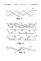
- FIG. 1 is a plan view showing a thin-film wiring configured into a twisted-wire pair in accordance with a preferred embodiment of the present invention
- FIG. 2 is an exploded view of FIG. 1 including the thin-film layers
- FIG. 3 is a top perspective view of one of the thin-film wiring of FIG. 1;
- FIGS. 4, 5 and 6 are cross-sectional views showing exemplary embodiments of the twisted-wire pair of FIG. 1;
- FIG. 7 is a flowchart illustrating a fabrication sequence of the twisted-wire pair of FIG. 6;
- FIG. 8 is an exemplary package utilizing the thin-film microflex in accordance with a second embodiment of the present invention.
- FIGS. 9, 10 , 11 , 12 , and 13 are cross-sectional views showing exemplary embodiments of the thin-film microflex structures of FIG. 8;
- FIG. 14 is an exemplary package utilizing the twisted-wire pair of FIG. 6;
- FIGS. 15 and 16 are exemplary packages utilizing the twisted-wire pair of FIG. 5;
- FIG. 17 is a plan view of a semiconductor leadframe package using the twisted-wire pair of FIG. 1 in accordance with an embodiment of the present invention
- FIG. 18 is a cross-sectional view of a semiconductor package including two chips utilizing the twisted-wire pair of FIG. 6;
- FIGS. 19 and 20 are cross-sectional views of exemplary semiconductor packages using the twisted-wire pair of FIG. 5 for connections to other devices;
- FIG. 21 is a plan view of FIG. 19;
- FIG. 22 is a plan view of two chips connected with the twisted-wire pair of FIG. 1;
- FIGS. 23, 24 and 25 are cross-sectional views of chip-scale packaging utilizing the twisted-wire pair of FIG. 5;
- FIG. 26 is a plan view of a vertical leadframe package using the twisted-wire pair of FIG. 1 in accordance with an embodiment of the present invention.
- FIGS. 27 and 28 are cross-sectional views of stacked chip packaging utilizing the twisted-wire pair of FIG. 5 .
- the twisted-wire pair 10 comprises termination pad 15 , thin-film wire having a middle portion and end portions made from a top layer of thin-film 14 , a thin-film wire having a middle portion and end portions made from a bottom layer of thin-film 12 and vias, or studs 18 , in an interconnection layer of thin-film connecting the end portions of the top layer thin-film wire 14 to the end portions of the bottom layer thin-film wire 12 , wherein the middle portions of the top and bottom layer cross each other.
- FIG. 2 illustrates each of the layers—top 14 , interconnection 18 and bottom 12 , with ihe respective thin-film wiring.
- FIG. 3 shows one completed wire fabricated from the top layer 14 , interconnection layer 18 and bottom layer 12 of thin-film, extending from termination pad to termination pad.
- the twisted-wire pair is the preferred embodiment of this invention, it is to be understood that other wiring and/or elements may also be made from the microflex thin-film, such as a single wire, capacitors, resistors, etc., which will be discussed in reference to FIGS. 9-13 below.
- the microflex connectors greatly enhance electrical performance and compactability in semiconductor packaging. As will be seen in subsequent examples, replacing long inner leads with a microflex twisted-pair wire in semiconductor leadframe packaging reduces the inner-lead inductance, thus enhancing the electrical performance, and reduces package stresses since the chip connects mechanically to a more compliant material. This enables new product applications for larger, higher I/O and more electrically-enhanced chips.
- FIGS. 4-7 illustrate exemplary procedures in fabricating a microflex twisted-wire pair for semiconductor packaging, wherein FIG. 7 is a flowchart depicting the process of fabricating FIG. 6 .
- metal lines 22 and 26 are plated onto a kapton carrier 28 and an inter-layer connection is made using plated thru-holes 24 .
- the resulting flexible, thin-film wire 20 A is similar to the microflex thin-film wire 10 of FIG. 3, except that thin-film wire 20 A is generally larger than the microflex thin-film wire 10 and will thus differ from microflex thin-film wire 10 in electrical characteristics and wiring ground rules.
- FIG. 5 illustrates a cross-section of a microflex twisted-wire pair 20 B just prior to release from silicon wafer carrier 30 .
- the twisted-wire pair 20 B comprises dielectric layers 32 , passivation layers 38 , barrier layer 36 , release layer 34 , and silicon wafer carrier 30 .
- the resulting twisted-wire pair is a free-standing microflex wire.
- FIG. 6 illustrates an example of fabricating a microflex twisted-wire pair 20 C, or other microflex connectors (hereinafter referred to as microflex), wherein the microflex may be in contact, both mechanically and electrically, to a dielectric or other substrate (e.g., an outer lead in a leadframe) via substrate connection 42 and may also comprise a free-standing microflex 50 .
- the free-standing microflex 50 is formed by etching away 44 substrate 40 .
- the free-standing microflex 50 may then be mechanically coupled to the top surface of the chip through adhesives, lamination etc.
- a microflex/leadframe structure as discussed in reference to FIGS. 8-12 below may also be fabricated by mechanically and electrically coupling the microflex to the leadframe/microflex substrate. This coupling allows the utilization of standard plastic encapsulated packing tooling and processing.
- FIG. 7 is a flowchart 100 illustrating a process by which a microflex/leadframe structure, such as one in FIG. 6, may be fabricated.
- the first step (step 102 ) includes coating a substrate (metal) sheet with a first thin-film dielectric layer, such as a photodcfineable epoxy or polyimide. Then, the first thin-film dielectric layer is exposed and developed (step 104 ) to form vias for connection between the substrate and the microflex wiring (including twisted-wire pair wiring) and cleared areas and openings. If necessary, a cure is applied (step 106 ), and then a first thin-film metal is deposited (step 108 ).
- a first thin-film dielectric layer such as a photodcfineable epoxy or polyimide.
- the thin-film metal is coated with photoresist (step 108 ) and the metal is exposed and developed (step 110 ) to create metal lines.
- a second thin-film dielectric layer, such as a passivation layer is then applied (step 112 ), vias are developed (step 114 ) and a cure is applied (step 116 ).
- a second thin-film metal layer is then deposited (step 118 ), and is coated with photoresist (step 120 ).
- step 124 no
- the microflex side of the microflex/leadframe structure is protected (step 126 ) and photoresist is deposited on the bottom side of the structure (step 128 ).
- the substrate (metal) features are then defined and etched (step 130 ) and the microflex protection layer is removed (step 132 ).
- the steps enclosed by box 113 may be repeated depending upon the layers of microflex desired.
- microflex separate from the metal substrate (such as in FIG. 5 ).
- the free-standing microflex can then be mechanically and electrically coupled either to a patterned or unpatterned leadframe, or used in other applications, such as chip-scale packaging, and stacked-chip packaging as discussed below.
- FIG. 8 illustrates a semiconductor package 21 A wherein chip 60 is electrically connected to the outer lead 56 through microflex 45 .
- Microflex 45 is fabricated with an opening which enables a wirebond connection 53 to connect to the I/O pads of chip 60 .
- Chip 60 , lead frame 56 , microflex 45 , and wirebond 53 assembly is encapsulated in plastic 54 , forming semiconductor package 21 A.
- Adhesive film 62 is placed between chip 60 and microflex 45 .
- FIGS. 9-13 illustrate exemplary microflex 45 that may be utilized in FIG. 8 .
- a microflex twisted-wire pair 55 is used to electrically connect chip 60 to outer lead 56 .
- An electrical connection 52 connects microflex 55 to outer lead 56 .
- microflex twisted-wire pair 55 replaces the long inner leads in semiconductor leadframe packaging and thus reduces the inner-lead inductance.
- FIG. 10 illustrates a microflex connector 45 having an integrated resistor 41 .
- Integrated resistor 41 is formed through the incorporation of a high resistance link 41 in the thin-film. This resistance link is used for enhanced electrical performance where circuit inductance is high. Thus, the input is dampened when there is too much inductance, allowing for a high performance system.
- FIG. 11 illustrates a microflex connector 45 with an integrated capacitor 41 in parallel with the power supply, and located between power supply and ground.
- a three level thin-film capacitor e.g., metal-polyimide-metal
- a wirebond 48 is shown, which couples the microflex to the chip 60 (FIG. 8 ).
- Capacitor 41 may also be created with two levels of metal.
- FIG. 12 shows a microflex connector 45 that allows for C4 connections with discrete devices, such as discrete device 46 .
- Discrete device 46 may be connected to any portion of microflex connector 45 , such as a middle portion.
- a discrete device may be electrically connected to chip 60 (FIG. 8) through microflex connector 45 .
- the discrete device characteristics may include passive circuitry (e.g., capacitor, resistor, or diode) and/or active circuitry.
- FIG. 13 shows a microflex connector 45 that allows for the connection of a discrete device 47 A through a fillet interconnection 47 B.
- a discrete device 47 A typical of industry-standard surface mount technology (SMT).
- SMT surface mount technology
- the discrete device may be electrically connected to chip 60 (FIG. 8 ).
- FIG. 14 illustrates a semiconductor package 21 B wherein chip 60 is electrically connected to the outer lead 56 through microflex 55 , which is similar to microflex 20 C of FIG. 6 .
- Microflex 55 is fabricated with an opening which enables a solder ball (C4) connection 64 to connect to the I/O pads of chip 60 .
- An electrical connection 52 connects microflex 55 to outer lead 56 .
- a plastic encapsulation 54 encloses semiconductor package 21 B.
- one of the many advantage of the present invention is the ability of utilizing C4 technology with leadframes and plastic encapsulation. This combination is possible because of the microflex technology of the present invention.
- FIGS. 15 and 16 illustrate semiconductor packages 23 A and 23 B wherein microflex 55 is attached to (as a free-standing microflex such as in FIG. 5) or fabricated on a carrier/support 58 .
- the outer leads 56 are electrically coupled to microflex 55 via wirebonding 53 and also mechanically coupled to microflex 55 and carrier/support 58 .
- FIG. 15 shows a wirebond connection 57 electrically connecting chip 60 to microflex 55 .
- FIG. 16 illustrates a solder ball connection 64 electrically connecting chip 60 to microflex 55 .
- FIG. 17 illustrates a top-down view of a semiconductor package similar to one depicted in FIG. 8 .
- the microflex leadframe structure depicted in FIG. 17 is fabricated using the process outlined in FIG. 7, built on metal substrate 71 .
- Cross-hatched region 68 is the microflex region, which contains microflex, such is twisted-wire pair, line/ground plane, microflex with a capacitor, etc.
- the leadframe support (element 58 of FIG. 8) is depicted by lines 72 .
- Region 66 portrays the outer lead regions (containing outer lead 56 of FIG. 8 ).
- the microflex electrically connects the package to leads 66 .
- the package may be wirebonded to leads through a wirebond pad array 70 .
- FIG. 18 illustrates combining chip-on-chip component technology (e.g., chip-on-chip component technology as disclosed in IBM patent disclosure BU9-97-063 referenced above) and microflex technology.
- a first chip 60 connects to a second chip 80 through C4 connections 64 .
- C4 connectors are specifically shown, other appropriate connectors may also be used to interconnect the chips, such as solder bumps, PMC paste, conductive epoxy, anisotropic conductive adhesive, etc.
- microflex 55 is electrically connected to chip 80 via wirebonding 53 and mechanically bonded to chip 80 via adhesive 74 .
- nicroflex 55 provides electrical signals to/from outer lead 56 from/to both chip 80 and chip 60 .
- FIG. 19 illustrates semiconductor package 67 comprising chip 60 , microflex 55 and encapsulation 54 .
- FIG. 21 illustrates the top-down view of semiconductor package 67 of FIG. 19 .
- microflex 55 comprises bare metal outer leads and thus may also function as part of semiconductor package 67 , enabling interconnection between chip 60 and the next level of assembly.
- the electrical and mechanical performance advantages of microflex technology such as a reduction in lead inductance and reduction in package stresses, are realized and enhanced.
- thermal management problems are minimized through the enhanced electrical performance of the package and through chip 60 , which being exposed in this package improves heat transfer.
- FIGS. 20 and 22 two chips, chip 60 and chip 80 , are interconnected and attached to microflex 55 , forming a semiconductor package.
- FIG. 20 illustrates the attachment of chips 60 and 80 to two sides of microflex 55 through C4 connectors.
- FIG. 22 is a top-down view of a generic semiconductor package comprising chips 60 and 80 interconnected with microflex 55 , such as twisted-wire pair to reduce inductance.
- FIGS. 23-25 illustrate exemplary chip-scale packaging utilizing microflex technology.
- chip 60 (chip 90 in FIG. 24) is electrically connected to microflex 55 through wirebond 53 , and is mechanically connected to microflex 55 through adhesive 74 .
- An encapsulant 54 is used on the exposed side of chip 60 .
- Microflex 55 wraps around chip 60 and provides a high electrical performance connection between chip 60 and the next level of packaging through electrical connectors 64 such as solder ball arrays.
- Adhesive 74 may be selected to achieve enhanced solder ball fatigue performance.
- solder ball encapsulant For example, if a silicone-based adhesive is used, then the differential thermal expansion between chip 60 and the substrate (not shown) to which the chip-scale package is connected can be accommodated without the use of a solder ball encapsulant. This feature enables removal and replacement of the chip-scale packages, which is particularly important for chip-on-chip component applications wherein component removal and replacement is critical to achieving overall module yields. Solder balls also allow for a continuous contact to the chip I/O throughout an entire burn-in process. If the electrical connectors 64 happen to be wirebond connectors, the wirebond pads may easily be converted to solder balls, and visa versa.
- chip 90 may shrink 91 without affecting the electrical connectors 64 .
- microflex 55 in a chip-scale package provides a low-cost module since the entire package does not need to be redesigned to accommodate any shrinkage.
- chip 80 is connected to chip 60 , which is coupled to microflex 55 .
- a wirebond encapsulant 69 and solder ball encapsulant 65 protects the exposed sections of the chip assembly.
- chip 80 being an SRAM and chip 60 being a microprocessor. Merging logic and memory chips can provide significantly enhanced electrical performance compared with current technology.
- a leadframe package 140 is shown in FIG. 26.
- a chip in package 140 may be wirebonded to leads 148 through wirebonds 152 .
- Micro flex 145 electrically connects the chip within package 140 to leads 148 .
- An opening 154 in microflex 145 allows for wirebonding to the chip.
- Support structures 144 support microflex 145 .
- three different microflex connectors are used: thin-film wiring 146 , a twisted-wire pair 155 and microflex with a resistor 142 .
- FIGS. 27 and 28 illustrate a stacked chip structure 160 that utilizes microflex 176 to allow for compaction and high performance of the stacked chips 161 .
- stacked chips 161 are separated by glue line 162 , in which is inserted a transfer metal 164 .
- the transfer metal 164 connects to a C4 solder ball 170 through C4 pad 168 .
- a C4 pad 172 in microflex 176 allows for each chip 161 to connect to a bond pad 180 , or wire bond 178 through thin-film wiring 174 in microflex and microflex 176 .
- An adhesive 182 connects one face of chip 161 to microflex 176 .
- FIG. 28 illustrates the microflex region comprising C4 pads 172 , thin-film wiring 174 , twisted-wire pair 176 and bond pad 180 , which wrap around chips 161 .
- microflex technology One of the key advantages of the microflex technology is that superior electrical performance (compared with currently available technologies) is possible. This superior electrical performance includes reduced line inductance, incorporation of integrated passive components, and attachment of discrete passive and active components to the microflex. All of these features enable operation of the chip at increased frequencies.
- microflex technology allow for enhanced electrical, mechanical and thermal performance in semiconductor packages.
- microflex technology allows for personalization of chips and packages by providing various chip-to-microflex interconnection configurations, as seen from the embodiments and examples of the present invention, increasing the ability to offer customer-specific personalization at a low-cost.
Abstract
Description
Claims (32)
Priority Applications (3)
| Application Number | Priority Date | Filing Date | Title |
|---|---|---|---|
| US09/105,382 US6300687B1 (en) | 1998-06-26 | 1998-06-26 | Micro-flex technology in semiconductor packages |
| US09/894,692 US6455778B2 (en) | 1998-06-26 | 2001-06-28 | Micro-flex technology in semiconductor packages |
| US09/894,706 US6444490B2 (en) | 1998-06-26 | 2001-06-28 | Micro-flex technology in semiconductor packages |
Applications Claiming Priority (1)
| Application Number | Priority Date | Filing Date | Title |
|---|---|---|---|
| US09/105,382 US6300687B1 (en) | 1998-06-26 | 1998-06-26 | Micro-flex technology in semiconductor packages |
Related Child Applications (2)
| Application Number | Title | Priority Date | Filing Date |
|---|---|---|---|
| US09/894,692 Division US6455778B2 (en) | 1998-06-26 | 2001-06-28 | Micro-flex technology in semiconductor packages |
| US09/894,706 Division US6444490B2 (en) | 1998-06-26 | 2001-06-28 | Micro-flex technology in semiconductor packages |
Publications (1)
| Publication Number | Publication Date |
|---|---|
| US6300687B1 true US6300687B1 (en) | 2001-10-09 |
Family
ID=22305515
Family Applications (3)
| Application Number | Title | Priority Date | Filing Date |
|---|---|---|---|
| US09/105,382 Expired - Fee Related US6300687B1 (en) | 1998-06-26 | 1998-06-26 | Micro-flex technology in semiconductor packages |
| US09/894,706 Expired - Fee Related US6444490B2 (en) | 1998-06-26 | 2001-06-28 | Micro-flex technology in semiconductor packages |
| US09/894,692 Expired - Fee Related US6455778B2 (en) | 1998-06-26 | 2001-06-28 | Micro-flex technology in semiconductor packages |
Family Applications After (2)
| Application Number | Title | Priority Date | Filing Date |
|---|---|---|---|
| US09/894,706 Expired - Fee Related US6444490B2 (en) | 1998-06-26 | 2001-06-28 | Micro-flex technology in semiconductor packages |
| US09/894,692 Expired - Fee Related US6455778B2 (en) | 1998-06-26 | 2001-06-28 | Micro-flex technology in semiconductor packages |
Country Status (1)
| Country | Link |
|---|---|
| US (3) | US6300687B1 (en) |
Cited By (13)
| Publication number | Priority date | Publication date | Assignee | Title |
|---|---|---|---|---|
| US20020043702A1 (en) * | 2000-10-16 | 2002-04-18 | Samsung Electronics Co., Ltd. | Semiconductor package comprising substrate with mounting leads and manufacturing method therefor |
| US20020163062A1 (en) * | 2001-02-26 | 2002-11-07 | International Business Machines Corporation | Multiple material stacks with a stress relief layer between a metal structure and a passivation layer |
| US20030054583A1 (en) * | 2001-09-20 | 2003-03-20 | Eastman Kodak Company | Method for producing an image sensor assembly |
| US20030107138A1 (en) * | 2001-12-08 | 2003-06-12 | Micron Technology, Inc. | Die package |
| US20040009631A1 (en) * | 2002-07-10 | 2004-01-15 | Mike Connell | Semiconductor package with circuit side polymer layer and wafer level fabrication method |
| US20040084766A1 (en) * | 2002-10-30 | 2004-05-06 | Pei-Ying Shieh | System-in-a-package device |
| US20040238924A1 (en) * | 2003-05-27 | 2004-12-02 | Song Ho Uk | Semiconductor package |
| US20040256708A1 (en) * | 1999-08-17 | 2004-12-23 | Jicheng Yang | Multi-chip module with extension |
| US20050011669A1 (en) * | 2002-12-17 | 2005-01-20 | Finisar Corporation | Low temperature bonding of multilayer substrates |
| US6884707B1 (en) * | 2000-09-08 | 2005-04-26 | Gabe Cherian | Interconnections |
| US20070111386A1 (en) * | 2002-02-20 | 2007-05-17 | Kim Sarah E | Process of vertically stacking multiple wafers supporting different active integrated circuit (IC) devices |
| US9478515B1 (en) * | 2015-04-14 | 2016-10-25 | SK Hynix Inc. | Semiconductor packages including interconnection members |
| US20180006002A1 (en) * | 2015-05-14 | 2018-01-04 | Mediatek Inc. | Semiconductor chip package and fabrication method thereof |
Families Citing this family (15)
| Publication number | Priority date | Publication date | Assignee | Title |
|---|---|---|---|---|
| US6380623B1 (en) * | 1999-10-15 | 2002-04-30 | Hughes Electronics Corporation | Microcircuit assembly having dual-path grounding and negative self-bias |
| US20060255446A1 (en) | 2001-10-26 | 2006-11-16 | Staktek Group, L.P. | Stacked modules and method |
| US6914324B2 (en) * | 2001-10-26 | 2005-07-05 | Staktek Group L.P. | Memory expansion and chip scale stacking system and method |
| US7656678B2 (en) | 2001-10-26 | 2010-02-02 | Entorian Technologies, Lp | Stacked module systems |
| US7026708B2 (en) * | 2001-10-26 | 2006-04-11 | Staktek Group L.P. | Low profile chip scale stacking system and method |
| US7169685B2 (en) | 2002-02-25 | 2007-01-30 | Micron Technology, Inc. | Wafer back side coating to balance stress from passivation layer on front of wafer and be used as die attach adhesive |
| DK1579745T3 (en) * | 2002-10-08 | 2006-09-18 | Oticon As | Layered structure with electrical conductors for a body-worn device |
| US6888064B2 (en) | 2002-12-18 | 2005-05-03 | International Business Machines Corporation | Modular packaging arrangements and methods |
| TWI241000B (en) * | 2003-01-21 | 2005-10-01 | Siliconware Precision Industries Co Ltd | Semiconductor package and fabricating method thereof |
| US7423340B2 (en) * | 2003-01-21 | 2008-09-09 | Siliconware Precision Industries Co., Ltd. | Semiconductor package free of substrate and fabrication method thereof |
| US7033861B1 (en) * | 2005-05-18 | 2006-04-25 | Staktek Group L.P. | Stacked module systems and method |
| US7464359B2 (en) | 2006-03-27 | 2008-12-09 | International Business Machines Corporation | Method for re-routing an interconnection array to improve switching behavior in a single net and an associated interconnection array structure |
| US7417310B2 (en) | 2006-11-02 | 2008-08-26 | Entorian Technologies, Lp | Circuit module having force resistant construction |
| US8159052B2 (en) * | 2008-04-10 | 2012-04-17 | Semtech Corporation | Apparatus and method for a chip assembly including a frequency extending device |
| US10044085B2 (en) * | 2016-04-14 | 2018-08-07 | Wisconsin Alumni Research Foundation | Stretchable transmission lines and circuits for microwave and millimeter wave frequency wearable electronics |
Citations (16)
| Publication number | Priority date | Publication date | Assignee | Title |
|---|---|---|---|---|
| US3978516A (en) | 1974-01-02 | 1976-08-31 | Texas Instruments Incorporated | Lead frame assembly for a packaged semiconductor microcircuit |
| US4160274A (en) | 1976-12-20 | 1979-07-03 | Texas Instruments Incorporated | Single chip molded magnetic bubble memory package |
| US4890157A (en) * | 1986-01-31 | 1989-12-26 | Texas Instruments Incorporated | Integrated circuit product having a polyimide film interconnection structure |
| US5196725A (en) | 1990-06-11 | 1993-03-23 | Hitachi Cable Limited | High pin count and multi-layer wiring lead frame |
| US5221858A (en) | 1992-02-14 | 1993-06-22 | Motorola, Inc. | Tape automated bonding (TAB) semiconductor device with ground plane and method for making the same |
| US5245215A (en) * | 1982-01-11 | 1993-09-14 | Kabushiki Kaisha Toshiba | Multichip packaged semiconductor device and method for manufacturing the same |
| US5362257A (en) | 1993-07-08 | 1994-11-08 | The Whitaker Corporation | Communications connector terminal arrays having noise cancelling capabilities |
| US5365409A (en) | 1993-02-20 | 1994-11-15 | Vlsi Technology, Inc. | Integrated circuit package design having an intermediate die-attach substrate bonded to a leadframe |
| US5386141A (en) | 1992-03-31 | 1995-01-31 | Vlsi Technology, Inc. | Leadframe having one or more power/ground planes without vias |
| US5488257A (en) | 1992-02-18 | 1996-01-30 | Intel Corporation | Multilayer molded plastic package using mesic technology |
| USRE35353E (en) | 1991-05-16 | 1996-10-22 | Shinko Electric Ind. Co, Ltd. | Process for manufacturing a multi-layer lead frame |
| US5606199A (en) | 1994-10-06 | 1997-02-25 | Nec Corporation | Resin-molded type semiconductor device with tape carrier connection between chip electrodes and inner leads of lead frame |
| US5790380A (en) * | 1995-12-15 | 1998-08-04 | International Business Machines Corporation | Method for fabricating a multiple chip module using orthogonal reorientation of connection planes |
| US5990566A (en) * | 1998-05-20 | 1999-11-23 | Micron Technology, Inc. | High density semiconductor package |
| US6043557A (en) * | 1994-05-03 | 2000-03-28 | Phelps, Jr.; Douglas Wallace | Tape application platform and processes therefor |
| US6153929A (en) * | 1998-08-21 | 2000-11-28 | Micron Technology, Inc. | Low profile multi-IC package connector |
Family Cites Families (5)
| Publication number | Priority date | Publication date | Assignee | Title |
|---|---|---|---|---|
| US5283390A (en) * | 1992-07-07 | 1994-02-01 | W. L. Gore & Associates, Inc. | Twisted pair data bus cable |
| US5767441A (en) * | 1996-01-04 | 1998-06-16 | General Cable Industries | Paired electrical cable having improved transmission properties and method for making same |
| US5914534A (en) * | 1996-05-03 | 1999-06-22 | Ford Motor Company | Three-dimensional multi-layer molded electronic device and method for manufacturing same |
| US6139957A (en) * | 1998-08-28 | 2000-10-31 | Commscope, Inc. Of North Carolina | Conductor insulated with foamed fluoropolymer and method of making same |
| US6323427B1 (en) * | 1999-05-28 | 2001-11-27 | Krone, Inc. | Low delay skew multi-pair cable and method of manufacture |
-
1998
- 1998-06-26 US US09/105,382 patent/US6300687B1/en not_active Expired - Fee Related
-
2001
- 2001-06-28 US US09/894,706 patent/US6444490B2/en not_active Expired - Fee Related
- 2001-06-28 US US09/894,692 patent/US6455778B2/en not_active Expired - Fee Related
Patent Citations (16)
| Publication number | Priority date | Publication date | Assignee | Title |
|---|---|---|---|---|
| US3978516A (en) | 1974-01-02 | 1976-08-31 | Texas Instruments Incorporated | Lead frame assembly for a packaged semiconductor microcircuit |
| US4160274A (en) | 1976-12-20 | 1979-07-03 | Texas Instruments Incorporated | Single chip molded magnetic bubble memory package |
| US5245215A (en) * | 1982-01-11 | 1993-09-14 | Kabushiki Kaisha Toshiba | Multichip packaged semiconductor device and method for manufacturing the same |
| US4890157A (en) * | 1986-01-31 | 1989-12-26 | Texas Instruments Incorporated | Integrated circuit product having a polyimide film interconnection structure |
| US5196725A (en) | 1990-06-11 | 1993-03-23 | Hitachi Cable Limited | High pin count and multi-layer wiring lead frame |
| USRE35353E (en) | 1991-05-16 | 1996-10-22 | Shinko Electric Ind. Co, Ltd. | Process for manufacturing a multi-layer lead frame |
| US5221858A (en) | 1992-02-14 | 1993-06-22 | Motorola, Inc. | Tape automated bonding (TAB) semiconductor device with ground plane and method for making the same |
| US5488257A (en) | 1992-02-18 | 1996-01-30 | Intel Corporation | Multilayer molded plastic package using mesic technology |
| US5386141A (en) | 1992-03-31 | 1995-01-31 | Vlsi Technology, Inc. | Leadframe having one or more power/ground planes without vias |
| US5365409A (en) | 1993-02-20 | 1994-11-15 | Vlsi Technology, Inc. | Integrated circuit package design having an intermediate die-attach substrate bonded to a leadframe |
| US5362257A (en) | 1993-07-08 | 1994-11-08 | The Whitaker Corporation | Communications connector terminal arrays having noise cancelling capabilities |
| US6043557A (en) * | 1994-05-03 | 2000-03-28 | Phelps, Jr.; Douglas Wallace | Tape application platform and processes therefor |
| US5606199A (en) | 1994-10-06 | 1997-02-25 | Nec Corporation | Resin-molded type semiconductor device with tape carrier connection between chip electrodes and inner leads of lead frame |
| US5790380A (en) * | 1995-12-15 | 1998-08-04 | International Business Machines Corporation | Method for fabricating a multiple chip module using orthogonal reorientation of connection planes |
| US5990566A (en) * | 1998-05-20 | 1999-11-23 | Micron Technology, Inc. | High density semiconductor package |
| US6153929A (en) * | 1998-08-21 | 2000-11-28 | Micron Technology, Inc. | Low profile multi-IC package connector |
Non-Patent Citations (6)
| Title |
|---|
| IBM Technical Disclosure Bulletin, vol. 25 No. 10, Mar. 1983, Chip-on-Chip Module for Assembly, Spector et al., 5315-5316. |
| IBM Technical Disclosure Bulletin, vol. 26 No. 9, Feb. 1984, Interposer for Chip-on-Chip Module Attachment, Feinberg et al., 4590-4591. |
| IBM Technical Disclosure Bulletin, vol. 36 No. 12, Dec. 1993, Flex Interconnect of Multi-Chip Modules, 463-464. |
| IBM Technical Disclosure Bulletin, vol. 36, No. 12, Dec. 1993, Enhanced I/O Capability for Silicon on Silicon Using Solder Columns, 75-76. |
| IBM Technical Disclosure Bulletin, vol. 36, No. 12, Dec. 1993, Optical Flex Interconnect to Multi-Chip Modules, 669. |
| Novel Uses of Flexible Circuit Technology in High Performance Electronic Applications, DiStefano et al., Microelectronics International No. 39, Jan. 1996, 11-15. |
Cited By (28)
| Publication number | Priority date | Publication date | Assignee | Title |
|---|---|---|---|---|
| US20040256708A1 (en) * | 1999-08-17 | 2004-12-23 | Jicheng Yang | Multi-chip module with extension |
| US6884707B1 (en) * | 2000-09-08 | 2005-04-26 | Gabe Cherian | Interconnections |
| US20020043702A1 (en) * | 2000-10-16 | 2002-04-18 | Samsung Electronics Co., Ltd. | Semiconductor package comprising substrate with mounting leads and manufacturing method therefor |
| US20020163062A1 (en) * | 2001-02-26 | 2002-11-07 | International Business Machines Corporation | Multiple material stacks with a stress relief layer between a metal structure and a passivation layer |
| US20030054583A1 (en) * | 2001-09-20 | 2003-03-20 | Eastman Kodak Company | Method for producing an image sensor assembly |
| US20040164410A1 (en) * | 2001-12-08 | 2004-08-26 | Micron Technology, Inc. | Die package |
| US20030107138A1 (en) * | 2001-12-08 | 2003-06-12 | Micron Technology, Inc. | Die package |
| SG104291A1 (en) * | 2001-12-08 | 2004-06-21 | Micron Technology Inc | Die package |
| US20050253226A1 (en) * | 2001-12-08 | 2005-11-17 | Micron Technology, Inc. | Die package |
| US6919645B2 (en) | 2001-12-08 | 2005-07-19 | Micron Technology, Inc. | Die package |
| US6825572B2 (en) | 2001-12-08 | 2004-11-30 | Micron Technology, Inc. | Die package |
| US7489028B2 (en) | 2001-12-08 | 2009-02-10 | Micron Technology, Inc. | Die package |
| US20070111386A1 (en) * | 2002-02-20 | 2007-05-17 | Kim Sarah E | Process of vertically stacking multiple wafers supporting different active integrated circuit (IC) devices |
| US20040009631A1 (en) * | 2002-07-10 | 2004-01-15 | Mike Connell | Semiconductor package with circuit side polymer layer and wafer level fabrication method |
| US7537966B2 (en) | 2002-07-10 | 2009-05-26 | Micron Technology, Inc. | Method for fabricating board on chip (BOC) semiconductor package with circuit side polymer layer |
| US7479413B2 (en) | 2002-07-10 | 2009-01-20 | Micron Technology, Inc. | Method for fabricating semiconductor package with circuit side polymer layer |
| US6791168B1 (en) * | 2002-07-10 | 2004-09-14 | Micron Technology, Inc. | Semiconductor package with circuit side polymer layer and wafer level fabrication method |
| US6949834B2 (en) | 2002-07-10 | 2005-09-27 | Micron Technology, Inc. | Stacked semiconductor package with circuit side polymer layer |
| US20040171191A1 (en) * | 2002-07-10 | 2004-09-02 | Mike Connell | Stacked semiconductor package with circuit side polymer layer |
| US6995041B2 (en) | 2002-07-10 | 2006-02-07 | Micron Technology, Inc. | Semiconductor package with circuit side polymer layer and wafer level fabrication method |
| US20060292752A1 (en) * | 2002-07-10 | 2006-12-28 | Mike Connell | Method for fabricating board on chip (BOC) semiconductor package with circuit side polymer layer |
| US20040084766A1 (en) * | 2002-10-30 | 2004-05-06 | Pei-Ying Shieh | System-in-a-package device |
| US7259466B2 (en) * | 2002-12-17 | 2007-08-21 | Finisar Corporation | Low temperature bonding of multilayer substrates |
| US20050011669A1 (en) * | 2002-12-17 | 2005-01-20 | Finisar Corporation | Low temperature bonding of multilayer substrates |
| US20040238924A1 (en) * | 2003-05-27 | 2004-12-02 | Song Ho Uk | Semiconductor package |
| US9478515B1 (en) * | 2015-04-14 | 2016-10-25 | SK Hynix Inc. | Semiconductor packages including interconnection members |
| US20180006002A1 (en) * | 2015-05-14 | 2018-01-04 | Mediatek Inc. | Semiconductor chip package and fabrication method thereof |
| US10685943B2 (en) * | 2015-05-14 | 2020-06-16 | Mediatek Inc. | Semiconductor chip package with resilient conductive paste post and fabrication method thereof |
Also Published As
| Publication number | Publication date |
|---|---|
| US6444490B2 (en) | 2002-09-03 |
| US20010039074A1 (en) | 2001-11-08 |
| US20010035529A1 (en) | 2001-11-01 |
| US6455778B2 (en) | 2002-09-24 |
Similar Documents
| Publication | Publication Date | Title |
|---|---|---|
| US6300687B1 (en) | Micro-flex technology in semiconductor packages | |
| US8053278B2 (en) | Multi-chip package type semiconductor device | |
| US6343019B1 (en) | Apparatus and method of stacking die on a substrate | |
| US5384488A (en) | Configuration and method for positioning semiconductor device bond pads using additional process layers | |
| US7619313B2 (en) | Multi-chip module and methods | |
| US6239366B1 (en) | Face-to-face multi-chip package | |
| US5894165A (en) | Leads between chips assembly | |
| JP4808408B2 (en) | Multi-chip package, semiconductor device used for the same, and manufacturing method thereof | |
| KR101070913B1 (en) | Stacked die package | |
| US8012803B2 (en) | Vertically stacked pre-packaged integrated circuit chips | |
| US6528353B2 (en) | Chip stack-type semiconductor package and method for fabricating the same | |
| US6982485B1 (en) | Stacking structure for semiconductor chips and a semiconductor package using it | |
| US7129571B2 (en) | Semiconductor chip package having decoupling capacitor and manufacturing method thereof | |
| US20020096785A1 (en) | Semiconductor device having stacked multi chip module structure | |
| US20030025199A1 (en) | Super low profile package with stacked dies | |
| US20070007643A1 (en) | Semiconductor multi-chip package | |
| US20040173889A1 (en) | Multiple die package | |
| US6916682B2 (en) | Semiconductor package device for use with multiple integrated circuits in a stacked configuration and method of formation and testing | |
| US6791166B1 (en) | Stackable lead frame package using exposed internal lead traces | |
| US7154171B1 (en) | Stacking structure for semiconductor devices using a folded over flexible substrate and method therefor | |
| KR100788341B1 (en) | Chip Stacked Semiconductor Package | |
| KR100351925B1 (en) | stack-type semiconductor package | |
| KR19990051002A (en) | Laminated package and its manufacturing method | |
| KR19980044246A (en) | Semiconductor package structure | |
| KR950006129Y1 (en) | Semiconduct assembly device |
Legal Events
| Date | Code | Title | Description |
|---|---|---|---|
| AS | Assignment |
Owner name: INTERNATIONAL BUSINESS MACHINES CORPORATION, NEW Y Free format text: ASSIGNMENT OF ASSIGNORS INTEREST;ASSIGNORS:BERTIN, CLAUDE LOUIS;FERENCE, THOMAS GEORGE;HOWELL, WAYNE JOHN;AND OTHERS;REEL/FRAME:009487/0046;SIGNING DATES FROM 19980625 TO 19980626 |
|
| FEPP | Fee payment procedure |
Free format text: PAYOR NUMBER ASSIGNED (ORIGINAL EVENT CODE: ASPN); ENTITY STATUS OF PATENT OWNER: LARGE ENTITY |
|
| CC | Certificate of correction | ||
| FPAY | Fee payment |
Year of fee payment: 4 |
|
| REMI | Maintenance fee reminder mailed | ||
| LAPS | Lapse for failure to pay maintenance fees | ||
| STCH | Information on status: patent discontinuation |
Free format text: PATENT EXPIRED DUE TO NONPAYMENT OF MAINTENANCE FEES UNDER 37 CFR 1.362 |
|
| FP | Lapsed due to failure to pay maintenance fee |
Effective date: 20091009 |
|
| AS | Assignment |
Owner name: GLOBALFOUNDRIES U.S. 2 LLC, NEW YORK Free format text: ASSIGNMENT OF ASSIGNORS INTEREST;ASSIGNOR:INTERNATIONAL BUSINESS MACHINES CORPORATION;REEL/FRAME:036550/0001 Effective date: 20150629 |
|
| AS | Assignment |
Owner name: GLOBALFOUNDRIES INC., CAYMAN ISLANDS Free format text: ASSIGNMENT OF ASSIGNORS INTEREST;ASSIGNORS:GLOBALFOUNDRIES U.S. 2 LLC;GLOBALFOUNDRIES U.S. INC.;REEL/FRAME:036779/0001 Effective date: 20150910 |