US6300668B2 - High resistance integrated circuit resistor - Google Patents
High resistance integrated circuit resistor Download PDFInfo
- Publication number
- US6300668B2 US6300668B2 US09/375,852 US37585299A US6300668B2 US 6300668 B2 US6300668 B2 US 6300668B2 US 37585299 A US37585299 A US 37585299A US 6300668 B2 US6300668 B2 US 6300668B2
- Authority
- US
- United States
- Prior art keywords
- depth
- conductivity type
- substrate
- type region
- resistor
- Prior art date
- Legal status (The legal status is an assumption and is not a legal conclusion. Google has not performed a legal analysis and makes no representation as to the accuracy of the status listed.)
- Expired - Fee Related
Links
- 239000002019 doping agent Substances 0.000 claims abstract description 88
- 239000000758 substrate Substances 0.000 claims description 110
- 239000004065 semiconductor Substances 0.000 claims description 25
- 238000009792 diffusion process Methods 0.000 abstract description 21
- 238000000034 method Methods 0.000 abstract description 21
- 230000000873 masking effect Effects 0.000 abstract description 14
- 238000005468 ion implantation Methods 0.000 abstract description 10
- 238000004519 manufacturing process Methods 0.000 abstract description 2
- 239000007943 implant Substances 0.000 abstract 2
- 239000010410 layer Substances 0.000 description 16
- 235000012431 wafers Nutrition 0.000 description 13
- 230000005669 field effect Effects 0.000 description 3
- 229920002120 photoresistant polymer Polymers 0.000 description 3
- 239000007858 starting material Substances 0.000 description 3
- XUIMIQQOPSSXEZ-UHFFFAOYSA-N Silicon Chemical compound [Si] XUIMIQQOPSSXEZ-UHFFFAOYSA-N 0.000 description 2
- 239000003990 capacitor Substances 0.000 description 2
- 229910052710 silicon Inorganic materials 0.000 description 2
- 239000010703 silicon Substances 0.000 description 2
- 230000000295 complement effect Effects 0.000 description 1
- 230000008021 deposition Effects 0.000 description 1
- 238000001914 filtration Methods 0.000 description 1
- 239000012212 insulator Substances 0.000 description 1
- 239000000463 material Substances 0.000 description 1
- 229910052751 metal Inorganic materials 0.000 description 1
- 239000002184 metal Substances 0.000 description 1
- 229910001120 nichrome Inorganic materials 0.000 description 1
- 229910021420 polycrystalline silicon Inorganic materials 0.000 description 1
- 229920005591 polysilicon Polymers 0.000 description 1
- 239000002344 surface layer Substances 0.000 description 1
- 229910052715 tantalum Inorganic materials 0.000 description 1
- GUVRBAGPIYLISA-UHFFFAOYSA-N tantalum atom Chemical compound [Ta] GUVRBAGPIYLISA-UHFFFAOYSA-N 0.000 description 1
- 239000010409 thin film Substances 0.000 description 1
Images


Classifications
-
- H—ELECTRICITY
- H01—ELECTRIC ELEMENTS
- H01L—SEMICONDUCTOR DEVICES NOT COVERED BY CLASS H10
- H01L29/00—Semiconductor devices adapted for rectifying, amplifying, oscillating or switching, or capacitors or resistors with at least one potential-jump barrier or surface barrier, e.g. PN junction depletion layer or carrier concentration layer; Details of semiconductor bodies or of electrodes thereof ; Multistep manufacturing processes therefor
- H01L29/66—Types of semiconductor device ; Multistep manufacturing processes therefor
- H01L29/66007—Multistep manufacturing processes
- H01L29/66075—Multistep manufacturing processes of devices having semiconductor bodies comprising group 14 or group 13/15 materials
- H01L29/66083—Multistep manufacturing processes of devices having semiconductor bodies comprising group 14 or group 13/15 materials the devices being controllable only by variation of the electric current supplied or the electric potential applied, to one or more of the electrodes carrying the current to be rectified, amplified, oscillated or switched, e.g. two-terminal devices
- H01L29/66166—Resistors with PN junction
-
- H—ELECTRICITY
- H01—ELECTRIC ELEMENTS
- H01L—SEMICONDUCTOR DEVICES NOT COVERED BY CLASS H10
- H01L21/00—Processes or apparatus adapted for the manufacture or treatment of semiconductor or solid state devices or of parts thereof
- H01L21/70—Manufacture or treatment of devices consisting of a plurality of solid state components formed in or on a common substrate or of parts thereof; Manufacture of integrated circuit devices or of parts thereof
- H01L21/77—Manufacture or treatment of devices consisting of a plurality of solid state components or integrated circuits formed in, or on, a common substrate
- H01L21/78—Manufacture or treatment of devices consisting of a plurality of solid state components or integrated circuits formed in, or on, a common substrate with subsequent division of the substrate into plural individual devices
- H01L21/82—Manufacture or treatment of devices consisting of a plurality of solid state components or integrated circuits formed in, or on, a common substrate with subsequent division of the substrate into plural individual devices to produce devices, e.g. integrated circuits, each consisting of a plurality of components
- H01L21/822—Manufacture or treatment of devices consisting of a plurality of solid state components or integrated circuits formed in, or on, a common substrate with subsequent division of the substrate into plural individual devices to produce devices, e.g. integrated circuits, each consisting of a plurality of components the substrate being a semiconductor, using silicon technology
- H01L21/8232—Field-effect technology
- H01L21/8234—MIS technology, i.e. integration processes of field effect transistors of the conductor-insulator-semiconductor type
- H01L21/8238—Complementary field-effect transistors, e.g. CMOS
-
- H—ELECTRICITY
- H01—ELECTRIC ELEMENTS
- H01L—SEMICONDUCTOR DEVICES NOT COVERED BY CLASS H10
- H01L27/00—Devices consisting of a plurality of semiconductor or other solid-state components formed in or on a common substrate
- H01L27/02—Devices consisting of a plurality of semiconductor or other solid-state components formed in or on a common substrate including semiconductor components specially adapted for rectifying, oscillating, amplifying or switching and having at least one potential-jump barrier or surface barrier; including integrated passive circuit elements with at least one potential-jump barrier or surface barrier
- H01L27/04—Devices consisting of a plurality of semiconductor or other solid-state components formed in or on a common substrate including semiconductor components specially adapted for rectifying, oscillating, amplifying or switching and having at least one potential-jump barrier or surface barrier; including integrated passive circuit elements with at least one potential-jump barrier or surface barrier the substrate being a semiconductor body
- H01L27/06—Devices consisting of a plurality of semiconductor or other solid-state components formed in or on a common substrate including semiconductor components specially adapted for rectifying, oscillating, amplifying or switching and having at least one potential-jump barrier or surface barrier; including integrated passive circuit elements with at least one potential-jump barrier or surface barrier the substrate being a semiconductor body including a plurality of individual components in a non-repetitive configuration
- H01L27/0611—Devices consisting of a plurality of semiconductor or other solid-state components formed in or on a common substrate including semiconductor components specially adapted for rectifying, oscillating, amplifying or switching and having at least one potential-jump barrier or surface barrier; including integrated passive circuit elements with at least one potential-jump barrier or surface barrier the substrate being a semiconductor body including a plurality of individual components in a non-repetitive configuration integrated circuits having a two-dimensional layout of components without a common active region
- H01L27/0617—Devices consisting of a plurality of semiconductor or other solid-state components formed in or on a common substrate including semiconductor components specially adapted for rectifying, oscillating, amplifying or switching and having at least one potential-jump barrier or surface barrier; including integrated passive circuit elements with at least one potential-jump barrier or surface barrier the substrate being a semiconductor body including a plurality of individual components in a non-repetitive configuration integrated circuits having a two-dimensional layout of components without a common active region comprising components of the field-effect type
- H01L27/0629—Devices consisting of a plurality of semiconductor or other solid-state components formed in or on a common substrate including semiconductor components specially adapted for rectifying, oscillating, amplifying or switching and having at least one potential-jump barrier or surface barrier; including integrated passive circuit elements with at least one potential-jump barrier or surface barrier the substrate being a semiconductor body including a plurality of individual components in a non-repetitive configuration integrated circuits having a two-dimensional layout of components without a common active region comprising components of the field-effect type in combination with diodes, or resistors, or capacitors
-
- H—ELECTRICITY
- H01—ELECTRIC ELEMENTS
- H01L—SEMICONDUCTOR DEVICES NOT COVERED BY CLASS H10
- H01L29/00—Semiconductor devices adapted for rectifying, amplifying, oscillating or switching, or capacitors or resistors with at least one potential-jump barrier or surface barrier, e.g. PN junction depletion layer or carrier concentration layer; Details of semiconductor bodies or of electrodes thereof ; Multistep manufacturing processes therefor
- H01L29/66—Types of semiconductor device ; Multistep manufacturing processes therefor
- H01L29/86—Types of semiconductor device ; Multistep manufacturing processes therefor controllable only by variation of the electric current supplied, or only the electric potential applied, to one or more of the electrodes carrying the current to be rectified, amplified, oscillated or switched
- H01L29/8605—Resistors with PN junctions
-
- Y—GENERAL TAGGING OF NEW TECHNOLOGICAL DEVELOPMENTS; GENERAL TAGGING OF CROSS-SECTIONAL TECHNOLOGIES SPANNING OVER SEVERAL SECTIONS OF THE IPC; TECHNICAL SUBJECTS COVERED BY FORMER USPC CROSS-REFERENCE ART COLLECTIONS [XRACs] AND DIGESTS
- Y10—TECHNICAL SUBJECTS COVERED BY FORMER USPC
- Y10S—TECHNICAL SUBJECTS COVERED BY FORMER USPC CROSS-REFERENCE ART COLLECTIONS [XRACs] AND DIGESTS
- Y10S148/00—Metal treatment
- Y10S148/136—Resistors
Definitions
- the present invention relates to semiconductor integrated circuits and, more particularly, to fabrication of resistors during integrated circuit processing.
- Integrated circuit designers use a variety of components to implement desired circuit functionality. These components may include bipolar and field-effect transistors, junction diodes, capacitors, and resistors.
- Resistors are used for a wide variety of circuit applications in which resistance values are required to be quite large.
- a resistor might be used to limit the current between its terminals for a given applied voltage. Such an applied voltage might be due to electrostatic discharge (ESD) which can damage integrated circuits.
- ESD electrostatic discharge
- Resistors can also be used in reference circuits such as a bandgap voltage reference or as feedback elements in conjunction with operational amplifier circuits.
- Another application of the integrated circuit resistor is its use with an integrated circuit capacitor to form a characteristic time constant for signal frequency filtering applications. In order to pass very low frequencies, the desired product of the resistance and capacitance might be appreciable, demanding large resistance values. In low-power applications, large resistors are useful for limiting currents thereby reducing power consumption.
- CMOS complementary metal-oxide-semiconductor
- CMOS complementary metal-oxide-semiconductor
- CMOS complementary metal-oxide-semiconductor
- CMOS complementary metal-oxide-semiconductor
- resistors can be created from the polysilicon used to form the gate regions of metal-oxide-semiconductor field-effect transistors (MOSFETs), or from the diffused well regions in which MOSFETs are later created, or from the ion-implantation step used to create source and drain diffusion regions of MOSFETs.
- MOSFETs metal-oxide-semiconductor field-effect transistors
- the primary object of this invention is to increase the resistance obtained from a diffusion resistor without increasing the integrated circuit area dedicated to implement the resistance and without increasing the complexity of the integrated circuit process.
- the present invention describes a method for utilizing the ion-implanted dopants which form the source and drain regions of n-channel and p-channel transistors to form a diffusion resistor composed of a first dopant and of banded regions of a counterdopant.
- the resistance of a diffusion resistor can be increased without increasing the area on the integrated circuit die occupied by the resistor or increasing the process complexity of a standard CMOS process.
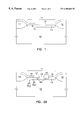
- FIG. 1 is a schematic cross-sectional view of a supporting substrate upon which a first dopant region has been created in an active area region, and a masking layer has been formed.
- FIG. 2A shows the view of FIG. 1 after the masking layer is patterned and etched, and after counterdopant regions have been formed.
- FIG. 2B shows a schematic top view of the preferred embodiment of the resistor.
- FIG. 2C shows a schematic top view of an alternative embodiment of the resistor.
- FIG. 2D shows a schematic top view of an alternative embodiment of the resistor.
- FIG. 2E shows a schematic cross-sectional view of an embodiment used as an alternative to FIG. 2 A.
- FIG. 3 shows the view of FIG. 2A after an insulating layer and contacts have been formed.
- FIG. 1 a cross-sectional view of a semiconductor substrate 10 is schematically shown.
- this substrate 10 is a p-type silicon wafer, however other types of wafers may also be used, including an n-type silicon wafer, a silicon-on-insulator (SOI) wafer, or a wafer with an epitaxially grown surface layer.
- active areas 11 are defined in which NMOS and PMOS field-effect transistors will be fabricated.
- a thick insulating Field-OXide (FOX) 12 is grown outside of these active areas 11 to isolate the transistors from each other.
- Active areas 11 are also defined where diffusion resistors will be fabricated. The shape of such active areas 11 will correspond to the diffusion resistor's shape on the surface of the semiconductor substrate 10 .
- first dopant region 13 is formed within an active area 11 .
- first dopant region 13 is formed by the same ion-implantation step used to simultaneously create n-type heavily doped (n+) NMOS transistor source/drain regions and n+ohmic contacts (guardbars) to contact n-type diffused well (n-well) regions created in substrate 10 as part of a conventional n-well CMOS process flow.
- a masking layer 14 has been deposited everywhere on the wafer of FIG. 1 .
- This photoresist (PR) masking layer 14 is used to mask the entire wafer except those regions defining MOS source/drains, those regions defining ohmic contacts (Quardbars) with doping type opposite to that of first dopant region 13 , and those regions where a counterdopant is to be introduced into the first dopant region 13 .
- PR photoresist
- the masking layer 14 has been patterned to form at least one opening 21 at least partially over the first dopant region 13 .
- Any opening 21 over first dopant region 13 has been used to define a counterdopant region 22 which at least partially intersects the first dopant region 13 .
- openings 21 do not intersect the first dopant region 13 .
- first dopant depth 23 the approximate depth of the first dopant region 13 is indicated by first dopant depth 23
- counterdopant depth 24 the approximate depth of the counterdopant region 22 is indicated by counterdopant depth 24 .
- These depths are approximate because the diffused junctions themselves are not abruptly defined, but graded. Also, these depths include a depletion region formed at the junction interface which depends on the voltage applied to the integrated circuit resistor.
- any counterdopant region 22 is created by the same ion-implantation step used to create PMOS source/drain diffusions and p-type heavily doped (p+) ohmic contact regions (guardbars) to contact substrate 10 .
- the first dopant region 13 may be created with the same p+ ion-implantation step used to create PMOS source/drain diffusions and p+ guardbars to contact p-type diffused well (p-well) regions created in substrate 10 as part of a conventional p-well CMOS process flow.
- the masking layer 14 defining openings 21 may be the same masking layer used to define NMOS source/drain diffusions and n+ guardbars to contact substrate 10 .
- any counterdopant region 22 may be created by the same ion-implantation step used to create NMOS source/drain diffusions and n+ guardbars to contact substrate 10 .
- first dopant region 13 could be contained within a p-well created by conventional p-well CMOS processing using n-type wafer as the starting material for substrate 10 .
- the first dopant region 13 may be created with the same ion-implantation step used to create NMOS source/drain diffusions and n+ guardbars to contact the n-type substrate 10 .
- the masking layer 14 defining openings 21 may be the same masking layer used to define PMOS source/drain diffusions and p+ guardbars to contact a p-well region created in substrate 10 as part of a conventional p-well process flow.
- any counterdopant region 22 may be created by the same ion-implantation step used to create PMOS source/drain diffusions and p+ guardbars to contact a p-well region created in substrate 10 as part of a conventional p-well process flow.
- first dopant region 13 could be contained within an n-well created by conventional n-well CMOS processing using a p-type wafer as starting material for substrate 10 .
- the first dopant region 13 may be created with the same ion-implantation step used to create PMOS source/drain diffusions and p+ guardbars to contact the p-type substrate 10 .
- the masking layer 14 defining openings 21 may be the same masking layer used to define NMOS source/drain diffusions and n+guardbars to contact an n-well region created in substrate 10 as part of a conventional n-well process flow.
- any counterdopant region 22 may be created by the same ion-implantation step used to create NMOS source/drain diffusions and n+ guardbars to contact an n-well region created in substrate 10 as part of a conventional n-well process flow.
- the relative doping concentrations of the first dopant region 13 and counterdopant region 22 can be described.
- the counterdopant region 22 has a higher doping concentration than the first dopant region 13 , forming junction diodes between the first dopant region 13 and the counterdopant region 22 .
- the counterdopant region 22 terminal of each junction diodes is left unconnected.
- current flow through the first dopant region 13 is pinched between counterdopant depth 24 and the substrate 10 .
- FIG. 2B shows a schematic top view of the preferred embodiment looking at the surface of the wafer.
- the surface area of the counterdopant region 22 is enclosed by the surface area of the first dopant region 13 .
- the top view of FIG. 2B is schematic only. If contacts to the first dopant region 13 are formed at points 25 and 26 , then the current through the first dopant region 13 between points 25 and 26 flows around the counterdopant regions 22 in those portions of the first dopant region 13 which are less deep than the counterdopant depth 24 . This pinching of the first dopant region 13 by the counterdopant regions 22 is therefore transverse to the direction of current flow between points 25 and 26 and parallel to the plane of the wafer's surface.
- FIG. 2C is a schematic top view of an alternate embodiment which shows the surface of the counterdopant region 22 extending outside the surface of the first dopant region 13 .
- This alternative embodiment results in further pinching of the first dopant region 13 by the counterdopant region 22 with this further pinching transverse to the direction of current flow between points 25 and 26 and parallel to the plane formed by the surface of the wafer.
- FIG. 2D is a schematic top view of an alternative embodiment which shows the surface of the counterdopant region 22 extending outside the surface of the first dopant region 13 such that current flow along the surface of the first dopant region 13 or at depths less than counterdopant depth 24 is completely blocked by at least one counterdopant region 22 .
- the pinching of the first dopant region is as shown in the cross-sectional view of FIG. 2A, between the counterdopant depth 24 and the substrate 10 .
- the counterdopant depth 24 exceeds the first dopant depth 23 .
- This alternative embodiment can be used in conjunction with either top view shown in FIG. 2B or FIG. 2 C.
- FIG. 2E cannot be used in conjunction with FIG. 2D since the junction diode formed by the boundary between counterdopant region 22 and first dopant region 13 will completely block current conduction through the first dopant region 13 .
- the counterdopant region 22 can have a lower doping concentration than the first dopant region 13 .
- junction diodes are not formed. Since the doping concentration of the counterdopant region 22 is lower than the doping concentration of the first dopant region 13 , the effective net doping type of the counterdopant regions 22 is the same type as the first dopant region 13 .
- Such counterdopant regions 22 do not create junction diodes, but instead present regions of lower effective doping concentration than the doping concentration of the first dopant region 13 . Since resistivity increases as doping concentration is lowered, the counterdopant regions 22 present regions of higher resistivity than presented by the first dopant region 13 alone. Since no diodes are formed, the schematic cross-sectional view of FIG. 2E can be used in conjunction with the top view of FIG. 2D when the first dopant concentration exceeds the counterdopant concentration.
- the masking layer 14 of FIG. 2 has been removed by conventional photoresist stripping techniques, and an insulating layer 30 has been deposited as part of a conventional CMOS process.
- Contact holes 31 have been created in insulating layer 30 as part of a conventional CMOS process and separate metal contacts 32 to first dopant region 13 have been created by conventional CMOS processing techniques.
Abstract
Description
Claims (39)
Priority Applications (1)
| Application Number | Priority Date | Filing Date | Title |
|---|---|---|---|
| US09/375,852 US6300668B2 (en) | 1996-02-01 | 1999-08-17 | High resistance integrated circuit resistor |
Applications Claiming Priority (4)
| Application Number | Priority Date | Filing Date | Title |
|---|---|---|---|
| US08/595,232 US5679593A (en) | 1996-02-01 | 1996-02-01 | Method of fabricating a high resistance integrated circuit resistor |
| US75339996A | 1996-11-26 | 1996-11-26 | |
| US08/963,103 US5990538A (en) | 1996-02-01 | 1997-11-03 | High resistivity integrated circuit resistor |
| US09/375,852 US6300668B2 (en) | 1996-02-01 | 1999-08-17 | High resistance integrated circuit resistor |
Related Parent Applications (1)
| Application Number | Title | Priority Date | Filing Date |
|---|---|---|---|
| US08/963,103 Continuation US5990538A (en) | 1996-02-01 | 1997-11-03 | High resistivity integrated circuit resistor |
Publications (2)
| Publication Number | Publication Date |
|---|---|
| US20010017396A1 US20010017396A1 (en) | 2001-08-30 |
| US6300668B2 true US6300668B2 (en) | 2001-10-09 |
Family
ID=24382353
Family Applications (3)
| Application Number | Title | Priority Date | Filing Date |
|---|---|---|---|
| US08/595,232 Expired - Lifetime US5679593A (en) | 1996-02-01 | 1996-02-01 | Method of fabricating a high resistance integrated circuit resistor |
| US08/963,103 Expired - Lifetime US5990538A (en) | 1996-02-01 | 1997-11-03 | High resistivity integrated circuit resistor |
| US09/375,852 Expired - Fee Related US6300668B2 (en) | 1996-02-01 | 1999-08-17 | High resistance integrated circuit resistor |
Family Applications Before (2)
| Application Number | Title | Priority Date | Filing Date |
|---|---|---|---|
| US08/595,232 Expired - Lifetime US5679593A (en) | 1996-02-01 | 1996-02-01 | Method of fabricating a high resistance integrated circuit resistor |
| US08/963,103 Expired - Lifetime US5990538A (en) | 1996-02-01 | 1997-11-03 | High resistivity integrated circuit resistor |
Country Status (1)
| Country | Link |
|---|---|
| US (3) | US5679593A (en) |
Cited By (8)
| Publication number | Priority date | Publication date | Assignee | Title |
|---|---|---|---|---|
| US20010049171A1 (en) * | 1998-05-20 | 2001-12-06 | Shigeki Onodera | High-cmos device having high-density resistance elements |
| US20050121746A1 (en) * | 2003-12-08 | 2005-06-09 | Erickson Sean C. | High performance diode implanted voltage controlled p-type diffusion resistor |
| US20050227430A1 (en) * | 2004-04-12 | 2005-10-13 | Chih-Feng Huang | Process of fabricating high resistance CMOS resistor |
| US20060057813A1 (en) * | 2004-09-15 | 2006-03-16 | Cheng-Hsiung Chen | Method of forming a polysilicon resistor |
| US20060226512A1 (en) * | 2005-04-01 | 2006-10-12 | Stmicroelectronics S.A. | Integrated circuit comprising a substrate and a resistor |
| US20070194390A1 (en) * | 2006-02-22 | 2007-08-23 | Chinthakindi Anil K | Method of fabricating a precision buried resistor |
| US20110198678A1 (en) * | 2010-02-12 | 2011-08-18 | United Microelectronics Corp. | Electrostatic discharge protection circuit |
| US10326028B1 (en) | 2018-01-08 | 2019-06-18 | Qualcomm Incorporated | Complementary metal-oxide-semiconductor (CMOS) voltage-controlled resistor |
Families Citing this family (11)
| Publication number | Priority date | Publication date | Assignee | Title |
|---|---|---|---|---|
| US5679593A (en) * | 1996-02-01 | 1997-10-21 | Micron Technology, Inc. | Method of fabricating a high resistance integrated circuit resistor |
| JPH10242394A (en) * | 1997-02-27 | 1998-09-11 | Matsushita Electron Corp | Fabrication of semiconductor device |
| JPH11297847A (en) * | 1998-04-13 | 1999-10-29 | Nec Kyushu Ltd | Semiconductor device and its manufacture |
| US20040092602A1 (en) * | 1998-05-07 | 2004-05-13 | Steiner Mitchell S. | Method for treatment and chemoprevention of prostate cancer |
| JP3244057B2 (en) | 1998-07-16 | 2002-01-07 | 日本電気株式会社 | Reference voltage source circuit |
| US6844600B2 (en) * | 1998-09-03 | 2005-01-18 | Micron Technology, Inc. | ESD/EOS protection structure for integrated circuit devices |
| US6331726B1 (en) | 2000-03-21 | 2001-12-18 | International Business Machines Corporation | SOI voltage dependent negative-saturation-resistance resistor ballasting element for ESD protection of receivers and driver circuitry |
| US6398348B1 (en) * | 2000-09-05 | 2002-06-04 | Hewlett-Packard Company | Printing structure with insulator layer |
| US20070176260A1 (en) * | 2006-01-31 | 2007-08-02 | Parekh Kunal R | Active area resistors and methods for making the same |
| US7589945B2 (en) * | 2006-08-31 | 2009-09-15 | Freescale Semiconductor, Inc. | Distributed electrostatic discharge protection circuit with varying clamp size |
| US7777998B2 (en) | 2007-09-10 | 2010-08-17 | Freescale Semiconductor, Inc. | Electrostatic discharge circuit and method therefor |
Citations (13)
| Publication number | Priority date | Publication date | Assignee | Title |
|---|---|---|---|---|
| US3629667A (en) * | 1969-03-14 | 1971-12-21 | Ibm | Semiconductor resistor with uniforms current distribution at its contact surface |
| US3735481A (en) | 1967-08-16 | 1973-05-29 | Hitachi Ltd | Method of manufacturing an integrated circuit having a transistor isolated by the collector region |
| US3795828A (en) | 1973-03-08 | 1974-03-05 | Ibm | Monolithic decoder circuit |
| US3879236A (en) | 1971-03-26 | 1975-04-22 | Ibm | Method of making a semiconductor resistor |
| US4418469A (en) | 1979-04-12 | 1983-12-06 | Matsushita Electric Industrial Co., Ltd. | Method of simultaneously forming buried resistors and bipolar transistors by ion implantation |
| US5001528A (en) | 1989-01-31 | 1991-03-19 | The United States Of America As Represented By The Secretary Of The Air Force | Radiation hardened CMOS on SOI or SOS devices |
| US5023195A (en) | 1989-05-19 | 1991-06-11 | Sanyo Electric Co., Ltd. | Method for manufacturing a semiconductor integrated circuit including a bipolar transistor |
| US5066602A (en) | 1982-04-19 | 1991-11-19 | Matsushita Electric Industrial Co., Ltd. | Method of making semiconductor ic including polar transistors |
| US5134088A (en) | 1990-04-27 | 1992-07-28 | Digital Equipment Corporation | Precision resistor in self-aligned silicided mos process |
| US5439841A (en) | 1994-01-12 | 1995-08-08 | Micrel, Inc. | High value gate leakage resistor |
| US5489547A (en) | 1994-05-23 | 1996-02-06 | Texas Instruments Incorporated | Method of fabricating semiconductor device having polysilicon resistor with low temperature coefficient |
| US5489796A (en) | 1992-03-30 | 1996-02-06 | Texas Instruments Incorporated | Integrated circuit resistor comprising amorphous silicon |
| US5990538A (en) * | 1996-02-01 | 1999-11-23 | Micron Technology, Inc. | High resistivity integrated circuit resistor |
Family Cites Families (3)
| Publication number | Priority date | Publication date | Assignee | Title |
|---|---|---|---|---|
| JPS59191369A (en) * | 1983-04-15 | 1984-10-30 | Hitachi Ltd | Resistance element for electronic device and manufacture thereof |
| JPH0251263A (en) * | 1988-08-13 | 1990-02-21 | Fujitsu Ltd | Semiconductor device |
| JPH0467666A (en) * | 1990-07-09 | 1992-03-03 | Fujitsu Ltd | Semiconductor device |
-
1996
- 1996-02-01 US US08/595,232 patent/US5679593A/en not_active Expired - Lifetime
-
1997
- 1997-11-03 US US08/963,103 patent/US5990538A/en not_active Expired - Lifetime
-
1999
- 1999-08-17 US US09/375,852 patent/US6300668B2/en not_active Expired - Fee Related
Patent Citations (13)
| Publication number | Priority date | Publication date | Assignee | Title |
|---|---|---|---|---|
| US3735481A (en) | 1967-08-16 | 1973-05-29 | Hitachi Ltd | Method of manufacturing an integrated circuit having a transistor isolated by the collector region |
| US3629667A (en) * | 1969-03-14 | 1971-12-21 | Ibm | Semiconductor resistor with uniforms current distribution at its contact surface |
| US3879236A (en) | 1971-03-26 | 1975-04-22 | Ibm | Method of making a semiconductor resistor |
| US3795828A (en) | 1973-03-08 | 1974-03-05 | Ibm | Monolithic decoder circuit |
| US4418469A (en) | 1979-04-12 | 1983-12-06 | Matsushita Electric Industrial Co., Ltd. | Method of simultaneously forming buried resistors and bipolar transistors by ion implantation |
| US5066602A (en) | 1982-04-19 | 1991-11-19 | Matsushita Electric Industrial Co., Ltd. | Method of making semiconductor ic including polar transistors |
| US5001528A (en) | 1989-01-31 | 1991-03-19 | The United States Of America As Represented By The Secretary Of The Air Force | Radiation hardened CMOS on SOI or SOS devices |
| US5023195A (en) | 1989-05-19 | 1991-06-11 | Sanyo Electric Co., Ltd. | Method for manufacturing a semiconductor integrated circuit including a bipolar transistor |
| US5134088A (en) | 1990-04-27 | 1992-07-28 | Digital Equipment Corporation | Precision resistor in self-aligned silicided mos process |
| US5489796A (en) | 1992-03-30 | 1996-02-06 | Texas Instruments Incorporated | Integrated circuit resistor comprising amorphous silicon |
| US5439841A (en) | 1994-01-12 | 1995-08-08 | Micrel, Inc. | High value gate leakage resistor |
| US5489547A (en) | 1994-05-23 | 1996-02-06 | Texas Instruments Incorporated | Method of fabricating semiconductor device having polysilicon resistor with low temperature coefficient |
| US5990538A (en) * | 1996-02-01 | 1999-11-23 | Micron Technology, Inc. | High resistivity integrated circuit resistor |
Cited By (19)
| Publication number | Priority date | Publication date | Assignee | Title |
|---|---|---|---|---|
| US6734075B2 (en) * | 1998-05-20 | 2004-05-11 | Mitsumi Electric Co., Ltd. | CMOS device having high-density resistance elements |
| US20010049171A1 (en) * | 1998-05-20 | 2001-12-06 | Shigeki Onodera | High-cmos device having high-density resistance elements |
| US6984869B2 (en) * | 2003-12-08 | 2006-01-10 | Lsi Logic Corporation | High performance diode implanted voltage controlled p-type diffusion resistor |
| US20050121746A1 (en) * | 2003-12-08 | 2005-06-09 | Erickson Sean C. | High performance diode implanted voltage controlled p-type diffusion resistor |
| US7169661B2 (en) * | 2004-04-12 | 2007-01-30 | System General Corp. | Process of fabricating high resistance CMOS resistor |
| US20070096255A1 (en) * | 2004-04-12 | 2007-05-03 | System General Corp. | High resistance cmos resistor |
| US20050227430A1 (en) * | 2004-04-12 | 2005-10-13 | Chih-Feng Huang | Process of fabricating high resistance CMOS resistor |
| US20060121684A1 (en) * | 2004-09-15 | 2006-06-08 | Cheng-Hsiung Chen | Method of forming a polysilicon resistor |
| US20060057813A1 (en) * | 2004-09-15 | 2006-03-16 | Cheng-Hsiung Chen | Method of forming a polysilicon resistor |
| US7714390B2 (en) | 2005-04-01 | 2010-05-11 | Stmicroelectronics S.A. | Integrated circuit comprising a substrate and a resistor |
| US20060226512A1 (en) * | 2005-04-01 | 2006-10-12 | Stmicroelectronics S.A. | Integrated circuit comprising a substrate and a resistor |
| US20070194390A1 (en) * | 2006-02-22 | 2007-08-23 | Chinthakindi Anil K | Method of fabricating a precision buried resistor |
| US7910450B2 (en) | 2006-02-22 | 2011-03-22 | International Business Machines Corporation | Method of fabricating a precision buried resistor |
| US20110108919A1 (en) * | 2006-02-22 | 2011-05-12 | International Business Machines Corporation | Method of fabricating a precision buried resistor |
| US20110198678A1 (en) * | 2010-02-12 | 2011-08-18 | United Microelectronics Corp. | Electrostatic discharge protection circuit |
| US8525265B2 (en) * | 2010-02-12 | 2013-09-03 | United Microelectronics Corp. | Electrostatic discharge protection circuit |
| US20130314826A1 (en) * | 2010-02-12 | 2013-11-28 | National Chiao Tung University | Electrostatic discharge protection circuit |
| US9190840B2 (en) * | 2010-02-12 | 2015-11-17 | United Microelectronics Corporation | Electrostatic discharge protection circuit |
| US10326028B1 (en) | 2018-01-08 | 2019-06-18 | Qualcomm Incorporated | Complementary metal-oxide-semiconductor (CMOS) voltage-controlled resistor |
Also Published As
| Publication number | Publication date |
|---|---|
| US5679593A (en) | 1997-10-21 |
| US20010017396A1 (en) | 2001-08-30 |
| US5990538A (en) | 1999-11-23 |
Similar Documents
| Publication | Publication Date | Title |
|---|---|---|
| US6300668B2 (en) | High resistance integrated circuit resistor | |
| US6249029B1 (en) | Device method for enhanced avalanche SOI CMOS | |
| US5717241A (en) | Gate controlled lateral bipolar junction transistor | |
| US5618688A (en) | Method of forming a monolithic semiconductor integrated circuit having an N-channel JFET | |
| US6445044B2 (en) | Apparatus improving latchup immunity in a dual-polysilicon gate | |
| TWI408779B (en) | Method of forming a semiconductor device and structure therefor | |
| US6746907B2 (en) | Methods of forming field effect transistors and field effect transistor circuitry | |
| US6365447B1 (en) | High-voltage complementary bipolar and BiCMOS technology using double expitaxial growth | |
| US5438005A (en) | Deep collection guard ring | |
| KR20090051213A (en) | Jfet with built in back gate in either soi or bulk silicon | |
| US5045900A (en) | Semiconductor device having a vertical power MOSFET fabricated in an isolated form on a semiconductor substrate | |
| KR920005539B1 (en) | Semiconductor overvoltage suppressor with accurately determined striking potential | |
| US10177045B2 (en) | Bulk CMOS RF switch with reduced parasitic capacitance | |
| JPH07130963A (en) | Monolithic integrated circuit and protective device | |
| US20040075529A1 (en) | High dopant conentration diffused resistor and method of manufacture therefor | |
| US6600205B2 (en) | Method for making low voltage transistors with increased breakdown voltage to substrate having three different MOS transistors | |
| US6777723B1 (en) | Semiconductor device having protection circuit implemented by bipolar transistor for discharging static charge current and process of fabrication | |
| US5070382A (en) | Semiconductor structure for high power integrated circuits | |
| US5965928A (en) | Semiconductor device with MOS capacitor and fabrication method thereof | |
| US5221635A (en) | Method of making a field-effect transistor | |
| US4547959A (en) | Uses for buried contacts in integrated circuits | |
| US4868621A (en) | Input protection circuit | |
| US6501152B1 (en) | Advanced lateral PNP by implant negation | |
| EP0627767B1 (en) | Process for fabricating JFET transistors and capacitors | |
| US6677208B2 (en) | Transistor with bottomwall/sidewall junction capacitance reduction region and method |
Legal Events
| Date | Code | Title | Description |
|---|---|---|---|
| FEPP | Fee payment procedure |
Free format text: PAYOR NUMBER ASSIGNED (ORIGINAL EVENT CODE: ASPN); ENTITY STATUS OF PATENT OWNER: LARGE ENTITY |
|
| FEPP | Fee payment procedure |
Free format text: PAYER NUMBER DE-ASSIGNED (ORIGINAL EVENT CODE: RMPN); ENTITY STATUS OF PATENT OWNER: LARGE ENTITY Free format text: PAYOR NUMBER ASSIGNED (ORIGINAL EVENT CODE: ASPN); ENTITY STATUS OF PATENT OWNER: LARGE ENTITY |
|
| FPAY | Fee payment |
Year of fee payment: 4 |
|
| FPAY | Fee payment |
Year of fee payment: 8 |
|
| REMI | Maintenance fee reminder mailed | ||
| LAPS | Lapse for failure to pay maintenance fees | ||
| STCH | Information on status: patent discontinuation |
Free format text: PATENT EXPIRED DUE TO NONPAYMENT OF MAINTENANCE FEES UNDER 37 CFR 1.362 |
|
| FP | Lapsed due to failure to pay maintenance fee |
Effective date: 20131009 |