US6285077B1 - Multiple layer tape ball grid array package - Google Patents
Multiple layer tape ball grid array package Download PDFInfo
- Publication number
- US6285077B1 US6285077B1 US09/377,887 US37788799A US6285077B1 US 6285077 B1 US6285077 B1 US 6285077B1 US 37788799 A US37788799 A US 37788799A US 6285077 B1 US6285077 B1 US 6285077B1
- Authority
- US
- United States
- Prior art keywords
- flexible tape
- package
- die
- traces
- tape
- Prior art date
- Legal status (The legal status is an assumption and is not a legal conclusion. Google has not performed a legal analysis and makes no representation as to the accuracy of the status listed.)
- Expired - Lifetime
Links
Images

Classifications
-
- H—ELECTRICITY
- H01—ELECTRIC ELEMENTS
- H01L—SEMICONDUCTOR DEVICES NOT COVERED BY CLASS H10
- H01L23/00—Details of semiconductor or other solid state devices
- H01L23/28—Encapsulations, e.g. encapsulating layers, coatings, e.g. for protection
- H01L23/31—Encapsulations, e.g. encapsulating layers, coatings, e.g. for protection characterised by the arrangement or shape
- H01L23/3107—Encapsulations, e.g. encapsulating layers, coatings, e.g. for protection characterised by the arrangement or shape the device being completely enclosed
- H01L23/3121—Encapsulations, e.g. encapsulating layers, coatings, e.g. for protection characterised by the arrangement or shape the device being completely enclosed a substrate forming part of the encapsulation
- H01L23/3128—Encapsulations, e.g. encapsulating layers, coatings, e.g. for protection characterised by the arrangement or shape the device being completely enclosed a substrate forming part of the encapsulation the substrate having spherical bumps for external connection
-
- H—ELECTRICITY
- H01—ELECTRIC ELEMENTS
- H01L—SEMICONDUCTOR DEVICES NOT COVERED BY CLASS H10
- H01L23/00—Details of semiconductor or other solid state devices
- H01L23/48—Arrangements for conducting electric current to or from the solid state body in operation, e.g. leads, terminal arrangements ; Selection of materials therefor
- H01L23/488—Arrangements for conducting electric current to or from the solid state body in operation, e.g. leads, terminal arrangements ; Selection of materials therefor consisting of soldered or bonded constructions
- H01L23/498—Leads, i.e. metallisations or lead-frames on insulating substrates, e.g. chip carriers
- H01L23/49833—Leads, i.e. metallisations or lead-frames on insulating substrates, e.g. chip carriers the chip support structure consisting of a plurality of insulating substrates
-
- H—ELECTRICITY
- H01—ELECTRIC ELEMENTS
- H01L—SEMICONDUCTOR DEVICES NOT COVERED BY CLASS H10
- H01L2224/00—Indexing scheme for arrangements for connecting or disconnecting semiconductor or solid-state bodies and methods related thereto as covered by H01L24/00
- H01L2224/01—Means for bonding being attached to, or being formed on, the surface to be connected, e.g. chip-to-package, die-attach, "first-level" interconnects; Manufacturing methods related thereto
- H01L2224/02—Bonding areas; Manufacturing methods related thereto
- H01L2224/04—Structure, shape, material or disposition of the bonding areas prior to the connecting process
- H01L2224/05—Structure, shape, material or disposition of the bonding areas prior to the connecting process of an individual bonding area
- H01L2224/0554—External layer
- H01L2224/05599—Material
-
- H—ELECTRICITY
- H01—ELECTRIC ELEMENTS
- H01L—SEMICONDUCTOR DEVICES NOT COVERED BY CLASS H10
- H01L2224/00—Indexing scheme for arrangements for connecting or disconnecting semiconductor or solid-state bodies and methods related thereto as covered by H01L24/00
- H01L2224/01—Means for bonding being attached to, or being formed on, the surface to be connected, e.g. chip-to-package, die-attach, "first-level" interconnects; Manufacturing methods related thereto
- H01L2224/42—Wire connectors; Manufacturing methods related thereto
- H01L2224/47—Structure, shape, material or disposition of the wire connectors after the connecting process
- H01L2224/48—Structure, shape, material or disposition of the wire connectors after the connecting process of an individual wire connector
- H01L2224/4805—Shape
- H01L2224/4809—Loop shape
- H01L2224/48091—Arched
-
- H—ELECTRICITY
- H01—ELECTRIC ELEMENTS
- H01L—SEMICONDUCTOR DEVICES NOT COVERED BY CLASS H10
- H01L2224/00—Indexing scheme for arrangements for connecting or disconnecting semiconductor or solid-state bodies and methods related thereto as covered by H01L24/00
- H01L2224/01—Means for bonding being attached to, or being formed on, the surface to be connected, e.g. chip-to-package, die-attach, "first-level" interconnects; Manufacturing methods related thereto
- H01L2224/42—Wire connectors; Manufacturing methods related thereto
- H01L2224/47—Structure, shape, material or disposition of the wire connectors after the connecting process
- H01L2224/48—Structure, shape, material or disposition of the wire connectors after the connecting process of an individual wire connector
- H01L2224/481—Disposition
- H01L2224/48151—Connecting between a semiconductor or solid-state body and an item not being a semiconductor or solid-state body, e.g. chip-to-substrate, chip-to-passive
- H01L2224/48221—Connecting between a semiconductor or solid-state body and an item not being a semiconductor or solid-state body, e.g. chip-to-substrate, chip-to-passive the body and the item being stacked
- H01L2224/48225—Connecting between a semiconductor or solid-state body and an item not being a semiconductor or solid-state body, e.g. chip-to-substrate, chip-to-passive the body and the item being stacked the item being non-metallic, e.g. insulating substrate with or without metallisation
- H01L2224/48227—Connecting between a semiconductor or solid-state body and an item not being a semiconductor or solid-state body, e.g. chip-to-substrate, chip-to-passive the body and the item being stacked the item being non-metallic, e.g. insulating substrate with or without metallisation connecting the wire to a bond pad of the item
-
- H—ELECTRICITY
- H01—ELECTRIC ELEMENTS
- H01L—SEMICONDUCTOR DEVICES NOT COVERED BY CLASS H10
- H01L2224/00—Indexing scheme for arrangements for connecting or disconnecting semiconductor or solid-state bodies and methods related thereto as covered by H01L24/00
- H01L2224/80—Methods for connecting semiconductor or other solid state bodies using means for bonding being attached to, or being formed on, the surface to be connected
- H01L2224/85—Methods for connecting semiconductor or other solid state bodies using means for bonding being attached to, or being formed on, the surface to be connected using a wire connector
- H01L2224/8538—Bonding interfaces outside the semiconductor or solid-state body
- H01L2224/85399—Material
-
- H—ELECTRICITY
- H01—ELECTRIC ELEMENTS
- H01L—SEMICONDUCTOR DEVICES NOT COVERED BY CLASS H10
- H01L24/00—Arrangements for connecting or disconnecting semiconductor or solid-state bodies; Methods or apparatus related thereto
- H01L24/01—Means for bonding being attached to, or being formed on, the surface to be connected, e.g. chip-to-package, die-attach, "first-level" interconnects; Manufacturing methods related thereto
- H01L24/42—Wire connectors; Manufacturing methods related thereto
- H01L24/47—Structure, shape, material or disposition of the wire connectors after the connecting process
- H01L24/48—Structure, shape, material or disposition of the wire connectors after the connecting process of an individual wire connector
-
- H—ELECTRICITY
- H01—ELECTRIC ELEMENTS
- H01L—SEMICONDUCTOR DEVICES NOT COVERED BY CLASS H10
- H01L2924/00—Indexing scheme for arrangements or methods for connecting or disconnecting semiconductor or solid-state bodies as covered by H01L24/00
- H01L2924/0001—Technical content checked by a classifier
- H01L2924/00014—Technical content checked by a classifier the subject-matter covered by the group, the symbol of which is combined with the symbol of this group, being disclosed without further technical details
-
- H—ELECTRICITY
- H01—ELECTRIC ELEMENTS
- H01L—SEMICONDUCTOR DEVICES NOT COVERED BY CLASS H10
- H01L2924/00—Indexing scheme for arrangements or methods for connecting or disconnecting semiconductor or solid-state bodies as covered by H01L24/00
- H01L2924/10—Details of semiconductor or other solid state devices to be connected
- H01L2924/11—Device type
- H01L2924/14—Integrated circuits
-
- H—ELECTRICITY
- H01—ELECTRIC ELEMENTS
- H01L—SEMICONDUCTOR DEVICES NOT COVERED BY CLASS H10
- H01L2924/00—Indexing scheme for arrangements or methods for connecting or disconnecting semiconductor or solid-state bodies as covered by H01L24/00
- H01L2924/15—Details of package parts other than the semiconductor or other solid state devices to be connected
- H01L2924/151—Die mounting substrate
- H01L2924/153—Connection portion
- H01L2924/1531—Connection portion the connection portion being formed only on the surface of the substrate opposite to the die mounting surface
- H01L2924/15311—Connection portion the connection portion being formed only on the surface of the substrate opposite to the die mounting surface being a ball array, e.g. BGA
-
- H—ELECTRICITY
- H01—ELECTRIC ELEMENTS
- H01L—SEMICONDUCTOR DEVICES NOT COVERED BY CLASS H10
- H01L2924/00—Indexing scheme for arrangements or methods for connecting or disconnecting semiconductor or solid-state bodies as covered by H01L24/00
- H01L2924/15—Details of package parts other than the semiconductor or other solid state devices to be connected
- H01L2924/181—Encapsulation
Definitions
- This invention relates generally to semiconductor integrated circuit packages, and more particularly to a flex tape ball grid array package.
- TBGA's Tape ball grid array packages
- TBGA's comprise a flexible plastic tape comprising a dielectric material, such as Kapton, and a metal pattern (traces) formed on the dielectric material.
- the metal pattern is connected to bond pads on an integrated circuit by a tape automated bonding process or some other process, such as wire bonding as is shown in co-pending application Ser. No. 08/837,686, filed Apr. 21, 1997.
- Each of the traces is connected to a solder ball, which serves as the electrical interface between the package and a printed circuit board. In this manner, integrated circuit bond pads in TBGA's are electrically coupled to an appropriate solder ball.
- the flexible tape material is relatively thin and therefore allows the entire package to be correspondingly thin and lightweight. These characteristics are beneficial for systems that are portable, such as cellular phones and other handheld electronic devices.
- the metal pattern mentioned above is typically constructed by laminating a metal foil layer to the tape material or by evaporating metal on the tape material. The metal pattern is then formed by selectively etching away the metal layer.
- the number of traces that may be created in this fashion for a given area of tape i.e. the density of traces
- the number of traces that may be created in this fashion for a given area of tape is limited by etch techniques. It would be desirable to increase the trace density of conventional TBGS'S.
- the present invention answers the above needs.
- the present invention comprises a package for an integrated circuit, comprising two layers (a top layer and a bottom layer) of flexible tape, each of which has a top surface and a bottom surface, with metal traces on the top surface.
- a die is mounted on top of the two layers and wire bonds connect bond pads on the die to metal traces on each of the two flexible tapes.
- the metal traces are routed along the top surfaces of the flexible tapes and are coupled to solder balls through holes in the tapes. These solder balls are mounted along the bottom of the package and serve as the electrical interface to a printed circuit board. Additional holes in the bottom layer tape allow solder balls to extend through the bottom layer tape so that they may be electrically coupled to traces on the top layer tape.
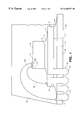
- FIG. 1 is a cross sectional view of an embodiment of the present invention.
- FIG. 2 is an overhead, cut-away view of the package shown in FIG. 1 .
- FIG. 1 is a cross sectional view of an embodiment of the present invention.
- a semiconductor package comprises a first flexible tape 14 that has a top surface 15 and a bottom surface 17 and a second flexible tape 16 that has a top surface 13 and a bottom surface 19 .
- the flexible tapes 14 and 16 preferably comprise Kapton.
- On each of the flexible tapes 14 and 16 there is a pattern of metal traces 30 and 32 (see FIG. 2) on the top surface 15 and 13 although the metal traces 30 and/or 32 may be on the bottom surfaces 17 and 19 or both the top surface 15 or 13 and the bottom surface 17 or 19 .
- holes 34 and 36 are etched or punched through the tape to allow for attaching solder balls (as will be described below) to pads 38 and 40 (see FIG. 2) on the top surface of the flexible tape substrate in question.
- a die 10 has a top surface 9 and a bottom surface 11 ; a plurality of bond pads 25 , shown as bond pads 25 a and 25 b , are on the top surface 9 . (For purposes of clarity, FIG. 1 omits most of the bond pads 25 .)
- the die 10 is mounted such that its bottom surface 11 faces the top surface 15 of the first flexible tape 14 . As shown in FIG. 2, an overhead cut-away view of the package, the die 10 is centered with respect to the first flexible tape 14 .
- An adhesive 12 serves to attach the die 10 to the first flexible tape 14 .
- a first set of 25 a of the bond pads 25 are connected by wires 22 to corresponding traces 30 on the first flexible tape 14 .
- the wires 22 may be attached to the traces 30 on the top surface 14 or, as further described in co-pending application, Ser. No. 08/837,686, filed Apr. 21, 1997, may be attached to traces on the bottom surface 17 through holes in the first flexible tape 14 .
- Each of a first plurality of solder balls 20 which serve as the electrical interface between the package and a printed circuit board, is electrically coupled to a corresponding one of the traces 30 on the first flexible tape 14 .
- Each of the first plurality of solder balls 20 extends through one of a plurality of holes 36 in the second flexible tape 16 .
- the second flexible tape 16 is mounted such that its top surface 13 faces the bottom surface 17 of the first flexible tape 14 .
- the first flexible tape 14 , second flexible tape 16 and the die 10 are thus arranged such that at least a portion of the first flexible tape 14 lies in a plane that is both (a) substantially parallel to both the bottom surface 11 of the die 10 and the top surface 13 of the second flexible tape 16 , and (b) between the bottom surface of the die 10 and the top surface of the second flexible tape 16 .
- An adhesive 26 serves to attach the first flexible tape 14 to the second flexible tape 16 .
- the length and width of the first flexible tape 14 are each smaller than the length and width of the second flexible tape 16 and the first flexible tape 14 is centered with respect to the second flexible tape 16 .
- a second set 25 b of the bond pads 25 are connected by wires 24 to corresponding traces 32 on the second flexible tape 16 .
- the wires 24 may be attached to the traces 32 on the top surface 13 or, as further described in copending application Ser. No. 08/837,686, filed Apr. 21, 1997, may be attached to traces on the bottom surface 19 through a hole in the second flexible tape 16 .
- Each of a second plurality of solder balls 18 around the periphery of the first plurality of solder balls 20 is electrically coupled to a corresponding one of the traces 32 on the second flexible tape 16 .
- a molding compound 28 covers the die 10 , the first flexible tape 14 and the second flexible tape 16 .
Abstract
Description
Claims (12)
Priority Applications (2)
| Application Number | Priority Date | Filing Date | Title |
|---|---|---|---|
| US09/377,887 US6285077B1 (en) | 1999-08-19 | 1999-08-19 | Multiple layer tape ball grid array package |
| JP2000248741A JP5069387B2 (en) | 1999-08-19 | 2000-08-18 | Integrated circuit package |
Applications Claiming Priority (1)
| Application Number | Priority Date | Filing Date | Title |
|---|---|---|---|
| US09/377,887 US6285077B1 (en) | 1999-08-19 | 1999-08-19 | Multiple layer tape ball grid array package |
Publications (1)
| Publication Number | Publication Date |
|---|---|
| US6285077B1 true US6285077B1 (en) | 2001-09-04 |
Family
ID=23490918
Family Applications (1)
| Application Number | Title | Priority Date | Filing Date |
|---|---|---|---|
| US09/377,887 Expired - Lifetime US6285077B1 (en) | 1999-08-19 | 1999-08-19 | Multiple layer tape ball grid array package |
Country Status (2)
| Country | Link |
|---|---|
| US (1) | US6285077B1 (en) |
| JP (1) | JP5069387B2 (en) |
Cited By (2)
| Publication number | Priority date | Publication date | Assignee | Title |
|---|---|---|---|---|
| US20030218245A1 (en) * | 2002-05-21 | 2003-11-27 | Hitachi, Ltd. | Semiconductor device and a method of manufacturing the same |
| CN100386873C (en) * | 2004-01-05 | 2008-05-07 | 扬智科技股份有限公司 | Wire bonding packaging body |
Citations (6)
| Publication number | Priority date | Publication date | Assignee | Title |
|---|---|---|---|---|
| US5844168A (en) * | 1995-08-01 | 1998-12-01 | Minnesota Mining And Manufacturing Company | Multi-layer interconnect sutructure for ball grid arrays |
| US5990545A (en) * | 1996-12-02 | 1999-11-23 | 3M Innovative Properties Company | Chip scale ball grid array for integrated circuit package |
| US6011694A (en) * | 1996-08-01 | 2000-01-04 | Fuji Machinery Mfg. & Electronics Co., Ltd. | Ball grid array semiconductor package with solder ball openings in an insulative base |
| US6048753A (en) * | 1996-04-02 | 2000-04-11 | Micron Technology, Inc. | Standardized bonding location process and apparatus |
| US6069407A (en) * | 1998-11-18 | 2000-05-30 | Vlsi Technology, Inc. | BGA package using PCB and tape in a die-up configuration |
| US6072700A (en) * | 1997-06-30 | 2000-06-06 | Hyundai Electronics Industries Co., Ltd. | Ball grid array package |
Family Cites Families (2)
| Publication number | Priority date | Publication date | Assignee | Title |
|---|---|---|---|---|
| JP2986413B2 (en) * | 1996-08-01 | 1999-12-06 | 富士機工電子株式会社 | AIRIA GRID ARRAY PACKAGE |
| US5866949A (en) * | 1996-12-02 | 1999-02-02 | Minnesota Mining And Manufacturing Company | Chip scale ball grid array for integrated circuit packaging |
-
1999
- 1999-08-19 US US09/377,887 patent/US6285077B1/en not_active Expired - Lifetime
-
2000
- 2000-08-18 JP JP2000248741A patent/JP5069387B2/en not_active Expired - Lifetime
Patent Citations (6)
| Publication number | Priority date | Publication date | Assignee | Title |
|---|---|---|---|---|
| US5844168A (en) * | 1995-08-01 | 1998-12-01 | Minnesota Mining And Manufacturing Company | Multi-layer interconnect sutructure for ball grid arrays |
| US6048753A (en) * | 1996-04-02 | 2000-04-11 | Micron Technology, Inc. | Standardized bonding location process and apparatus |
| US6011694A (en) * | 1996-08-01 | 2000-01-04 | Fuji Machinery Mfg. & Electronics Co., Ltd. | Ball grid array semiconductor package with solder ball openings in an insulative base |
| US5990545A (en) * | 1996-12-02 | 1999-11-23 | 3M Innovative Properties Company | Chip scale ball grid array for integrated circuit package |
| US6072700A (en) * | 1997-06-30 | 2000-06-06 | Hyundai Electronics Industries Co., Ltd. | Ball grid array package |
| US6069407A (en) * | 1998-11-18 | 2000-05-30 | Vlsi Technology, Inc. | BGA package using PCB and tape in a die-up configuration |
Cited By (3)
| Publication number | Priority date | Publication date | Assignee | Title |
|---|---|---|---|---|
| US20030218245A1 (en) * | 2002-05-21 | 2003-11-27 | Hitachi, Ltd. | Semiconductor device and a method of manufacturing the same |
| US6900551B2 (en) * | 2002-05-21 | 2005-05-31 | Renesas Technology Corp. | Semiconductor device with alternate bonding wire arrangement |
| CN100386873C (en) * | 2004-01-05 | 2008-05-07 | 扬智科技股份有限公司 | Wire bonding packaging body |
Also Published As
| Publication number | Publication date |
|---|---|
| JP2001077243A (en) | 2001-03-23 |
| JP5069387B2 (en) | 2012-11-07 |
Similar Documents
| Publication | Publication Date | Title |
|---|---|---|
| KR100546374B1 (en) | Multi chip package having center pads and method for manufacturing the same | |
| US7656044B2 (en) | Semiconductor device with improved resin configuration | |
| US6774473B1 (en) | Semiconductor chip module | |
| US6713856B2 (en) | Stacked chip package with enhanced thermal conductivity | |
| US6407448B2 (en) | Stackable ball grid array semiconductor package and fabrication method thereof | |
| US6002169A (en) | Thermally enhanced tape ball grid array package | |
| US6798049B1 (en) | Semiconductor package and method for fabricating the same | |
| KR100716871B1 (en) | Carrier frame for semiconductor package and semiconductor package using it and its manufacturing method | |
| US7501313B2 (en) | Method of making semiconductor BGA package having a segmented voltage plane | |
| US5869889A (en) | Thin power tape ball grid array package | |
| US5559305A (en) | Semiconductor package having adjacently arranged semiconductor chips | |
| US6225690B1 (en) | Plastic ball grid array package with strip line configuration | |
| US20020063331A1 (en) | Film carrier semiconductor device | |
| US6127728A (en) | Single reference plane plastic ball grid array package | |
| US6285077B1 (en) | Multiple layer tape ball grid array package | |
| US6057594A (en) | High power dissipating tape ball grid array package | |
| US7091594B1 (en) | Leadframe type semiconductor package having reduced inductance and its manufacturing method | |
| US20080308913A1 (en) | Stacked semiconductor package and method of manufacturing the same | |
| US20040125574A1 (en) | Multi-chip semiconductor package and method for manufacturing the same | |
| US6429534B1 (en) | Interposer tape for semiconductor package | |
| KR19980063740A (en) | Multilayer Leadframe for Molded Packages | |
| KR100549312B1 (en) | Semiconductor package and its manufacturing method | |
| US20040021213A1 (en) | Thermally-enhanced integrated circuit package | |
| KR100388291B1 (en) | Structure of semiconductor package | |
| KR100533762B1 (en) | Semiconductor package |
Legal Events
| Date | Code | Title | Description |
|---|---|---|---|
| STCF | Information on status: patent grant |
Free format text: PATENTED CASE |
|
| FPAY | Fee payment |
Year of fee payment: 4 |
|
| FEPP | Fee payment procedure |
Free format text: PAYOR NUMBER ASSIGNED (ORIGINAL EVENT CODE: ASPN); ENTITY STATUS OF PATENT OWNER: LARGE ENTITY |
|
| FPAY | Fee payment |
Year of fee payment: 8 |
|
| FPAY | Fee payment |
Year of fee payment: 12 |
|
| AS | Assignment |
Owner name: DEUTSCHE BANK AG NEW YORK BRANCH, AS COLLATERAL AG Free format text: PATENT SECURITY AGREEMENT;ASSIGNORS:LSI CORPORATION;AGERE SYSTEMS LLC;REEL/FRAME:032856/0031 Effective date: 20140506 |
|
| AS | Assignment |
Owner name: AVAGO TECHNOLOGIES GENERAL IP (SINGAPORE) PTE. LTD Free format text: ASSIGNMENT OF ASSIGNORS INTEREST;ASSIGNOR:LSI CORPORATION;REEL/FRAME:035390/0388 Effective date: 20140814 |
|
| AS | Assignment |
Owner name: LSI CORPORATION, CALIFORNIA Free format text: TERMINATION AND RELEASE OF SECURITY INTEREST IN PATENT RIGHTS (RELEASES RF 032856-0031);ASSIGNOR:DEUTSCHE BANK AG NEW YORK BRANCH, AS COLLATERAL AGENT;REEL/FRAME:037684/0039 Effective date: 20160201 Owner name: AGERE SYSTEMS LLC, PENNSYLVANIA Free format text: TERMINATION AND RELEASE OF SECURITY INTEREST IN PATENT RIGHTS (RELEASES RF 032856-0031);ASSIGNOR:DEUTSCHE BANK AG NEW YORK BRANCH, AS COLLATERAL AGENT;REEL/FRAME:037684/0039 Effective date: 20160201 |
|
| AS | Assignment |
Owner name: BANK OF AMERICA, N.A., AS COLLATERAL AGENT, NORTH CAROLINA Free format text: PATENT SECURITY AGREEMENT;ASSIGNOR:AVAGO TECHNOLOGIES GENERAL IP (SINGAPORE) PTE. LTD.;REEL/FRAME:037808/0001 Effective date: 20160201 Owner name: BANK OF AMERICA, N.A., AS COLLATERAL AGENT, NORTH Free format text: PATENT SECURITY AGREEMENT;ASSIGNOR:AVAGO TECHNOLOGIES GENERAL IP (SINGAPORE) PTE. LTD.;REEL/FRAME:037808/0001 Effective date: 20160201 |
|
| AS | Assignment |
Owner name: AVAGO TECHNOLOGIES GENERAL IP (SINGAPORE) PTE. LTD., SINGAPORE Free format text: TERMINATION AND RELEASE OF SECURITY INTEREST IN PATENTS;ASSIGNOR:BANK OF AMERICA, N.A., AS COLLATERAL AGENT;REEL/FRAME:041710/0001 Effective date: 20170119 Owner name: AVAGO TECHNOLOGIES GENERAL IP (SINGAPORE) PTE. LTD Free format text: TERMINATION AND RELEASE OF SECURITY INTEREST IN PATENTS;ASSIGNOR:BANK OF AMERICA, N.A., AS COLLATERAL AGENT;REEL/FRAME:041710/0001 Effective date: 20170119 |
|
| AS | Assignment |
Owner name: BELL SEMICONDUCTOR, LLC, ILLINOIS Free format text: ASSIGNMENT OF ASSIGNORS INTEREST;ASSIGNORS:AVAGO TECHNOLOGIES GENERAL IP (SINGAPORE) PTE. LTD.;BROADCOM CORPORATION;REEL/FRAME:044886/0766 Effective date: 20171208 |
|
| AS | Assignment |
Owner name: CORTLAND CAPITAL MARKET SERVICES LLC, AS COLLATERA Free format text: SECURITY INTEREST;ASSIGNORS:HILCO PATENT ACQUISITION 56, LLC;BELL SEMICONDUCTOR, LLC;BELL NORTHERN RESEARCH, LLC;REEL/FRAME:045216/0020 Effective date: 20180124 |
|
| AS | Assignment |
Owner name: BELL NORTHERN RESEARCH, LLC, ILLINOIS Free format text: RELEASE BY SECURED PARTY;ASSIGNOR:CORTLAND CAPITAL MARKET SERVICES LLC;REEL/FRAME:059723/0382 Effective date: 20220401 Owner name: BELL SEMICONDUCTOR, LLC, ILLINOIS Free format text: RELEASE BY SECURED PARTY;ASSIGNOR:CORTLAND CAPITAL MARKET SERVICES LLC;REEL/FRAME:059723/0382 Effective date: 20220401 Owner name: HILCO PATENT ACQUISITION 56, LLC, ILLINOIS Free format text: RELEASE BY SECURED PARTY;ASSIGNOR:CORTLAND CAPITAL MARKET SERVICES LLC;REEL/FRAME:059723/0382 Effective date: 20220401 |