US6271720B1 - Operational filter building block - Google Patents
Operational filter building block Download PDFInfo
- Publication number
- US6271720B1 US6271720B1 US09/305,132 US30513299A US6271720B1 US 6271720 B1 US6271720 B1 US 6271720B1 US 30513299 A US30513299 A US 30513299A US 6271720 B1 US6271720 B1 US 6271720B1
- Authority
- US
- United States
- Prior art keywords
- output terminal
- summing circuit
- input
- circuit
- coupled
- Prior art date
- Legal status (The legal status is an assumption and is not a legal conclusion. Google has not performed a legal analysis and makes no representation as to the accuracy of the status listed.)
- Expired - Lifetime
Links
Images


Classifications
-
- H—ELECTRICITY
- H03—ELECTRONIC CIRCUITRY
- H03H—IMPEDANCE NETWORKS, e.g. RESONANT CIRCUITS; RESONATORS
- H03H11/00—Networks using active elements
- H03H11/02—Multiple-port networks
- H03H11/04—Frequency selective two-port networks
Definitions
- This invention relates to electrical filters. More particularly, this invention relates to 2nd order cascadable active-RC filters.
- Electrical filters receive signals that typically oscillate between a maximum value and a minimum value (e.g., a sinusoidal signal). These signals are known as AC, or alternating current, signals. (In contrast, signals that maintain a substantially steady value are known as DC, or direct current, signals.) Each oscillation between a maximum and minimum value is a cycle, and the number of cycles per second is the frequency, which is measured in Hertz (one Hertz is one cycle per second). AC signals typically have more than one frequency component. These components can range from low frequencies to high frequencies (e.g., 100 Hz to 100k Hz).
- Electrical filters attenuate, or filter out, one or more undesired frequency components from an AC signal, while permitting other frequency components of the signal to pass through.
- different types of filters are used. For example, a low pass filter permits only frequencies below a cutoff frequency to pass through, while frequencies above the cutoff frequency are filtered out. Conversely, a high pass filter permits only frequencies above a cutoff frequency to pass through, while frequencies below the cutoff frequency are filtered out.
- Band-pass filters permit a range, or band, of frequencies (or only a single frequency) to pass through, while frequencies below a lower bandwidth-edge frequency and above an upper bandwidth-edge frequency are filtered out.
- band-reject or notch filters permit all frequencies except a band of frequencies (or only a single frequency) to pass through.
- the frequencies allowed to pass through the filter are said to be in the passband, while the filtered out frequencies are said to be in the stopband.
- Filters can be of different “orders.” For example, filters can be 2nd order low pass filters, 5th order low pass filters, 6th order band-pass filters, and 8th order high pass filters, among many others.
- the filter order relates mathematically to the transfer function of the filter.
- the filter transfer function is a ratio of the filter output to the filter input. Typically, this ratio is a function of signal frequency and phase.
- Filters of the 2nd order are useful because they can be cascaded to form higher order filters. Cascading is the coupling of filters into a series such that the output of one becomes the input of the next.
- Active filters provide signal gain and include passive elements and one or more active elements (e.g., transistor devices). Active elements have frequency dependent characteristics and are usually devices that are voltage-dependent or current-dependent. As is known in the art, active filters can be constructed with off-the-shelf operational amplifiers (op amps). However, such op amps usually require numerous external precision components, thus consuming large amounts of circuit board space. Moreover, precision components can be expensive.
- op amps off-the-shelf operational amplifiers
- Active filters of the 2nd order are characterized by various filter parameters, including center frequency (f O ), quality factor (Q), and filter gain. Cutoff frequencies, mentioned above with respect to low pass and high pass filters, are functions of the center frequency and quality factor. Furthermore, the center frequency, quality factor, and filter gain are functions of the various filter circuit elements, and can be calculated accordingly with known filter equations.
- Active filters are typically either available as standard off-the-shelf (usually discrete) circuit devices with fixed filter functions and parameters, or are custom designed as either discrete or integrated circuit devices. In either case, such filters usually cannot be easily modified or adjusted to meet application requirements other than those they were originally designed for. In other words, filter functions and parameters usually cannot be easily modified or adjusted once the filter is manufactured, because doing so usually requires either adding additional components and elements, replacing one or more existing circuit elements with different elements (e.g., replacing a resistor with a capacitor), replacing one or more existing elements with elements of different value (e.g., replacing a 10 k ohm resistor with a 150 k ohm resistor), or all of the above.
- replacing one or more existing circuit elements with different elements e.g., replacing a resistor with a capacitor
- replacing one or more existing elements with elements of different value e.g., replacing a 10 k ohm resistor with a 150 k ohm resistor
- FIG. 1A shows a known 2nd order filter that provides low pass and band-pass frequency responses.
- Filter 100 includes op amps 103 , 113 , and 123 ; resistors 101 , 107 , 109 , 111 , 117 , and 119 ; and capacitors 105 and 115 .
- Band-pass response V 1 is available at node 121
- low pass frequency responses V 2 and V 3 are respectively available at nodes 125 and 127 .
- values for each of the numerous circuit elements are determined based on a cumbersome series of known design equations.
- modifying filter 100 to perform other filtering functions can be equally difficult.
- the following circuit component and elements should be coupled to filter 100 , as shown in FIG. 1 B: op amp 139 and resistors 131 , 133 , 135 , and 137 . Additional calculations need to be performed to determine the values of resistors 131 , 133 , 135 , and 137 , and sufficient space needs to be available to add these parts.
- High pass frequency response V HP is then available at node 138 .
- the values of the other circuit elements of filter 130 may also need to be recalculated. This probably will require that one of more of these elements be replaced. Again, this process often is impractical if not impossible.
- notch filters such as filters 160 and 190 , shown respectively in FIGS. 1C and 1D, also cannot be easily modified or adjusted once constructed. Furthermore, constructing notch filters 160 and 190 with filters 100 or 130 is typically cumbersome and impractical.
- Notch filter 160 includes op amps 163 and 181 , integrators 171 and 173 , and resistors 161 , 165 , 167 , 169 , 175 , 177 , and 179 .
- Notch response V N1 is available at node 180 and, as shown in FIG. 1C., is obtained by summing high pass response V HP at node 164 with low pass response V LP at node 174 .
- R and C are the combined internal resistance and capacitance of integrators 171 and 173 .
- the values of resistors 165 , 169 , 175 , and 177 , and the RC value of integrators 171 and 173 accordingly determine the notch frequency, which can be higher, lower, or equal to the center frequency of notch filter 160 . Modifying the notch frequency will require replacement of one or more of these circuit elements, which again is often impractical even if filter 160 is a discrete device, and is more likely impossible if filter 160 is an integrated circuit.
- Known notch filter 190 provides notch frequency response V N2 by summing input signal V IN with inverting band-pass output response V BP as shown in FIG. 1 D.
- Notch filter 190 includes 2nd order inverting band-pass filter 191 (of which many circuit configurations are known), op amp 199 , and resistors 193 , 195 , and 197 .
- notch filter 190 requires only a few external components, filter 190 is limited to a notch frequency equaling the center As frequency.
- Another disadvantage of notch filter 190 is that if precision components are not used, the notch frequency will not be completely filtered out, which will result in some signal gain at that frequency.
- users are left with few choices for meeting particular filter applications. For example, users can search for an available off-the-shelf filter; laboriously modify, if possible, an existing filter; or custom design a new filter.
- a 3-terminal operational filter circuit includes an input terminal for receiving an input signal, a first output terminal for providing a first frequency response, and a second output terminal for providing a second frequency response.
- the filter circuit also includes an operational amplifier circuit, a capacitor, and a non-inverting integrator.
- the operational amplifier circuit has an inverting input, a non-inverting input and an amplifier output. The inverting input is coupled to the input terminal, the non-inverting input is coupled to ground, and the amplifier output is coupled to the second output terminal.
- the capacitor is coupled between the inverting input and the amplifier output.
- the input of the non-inverting integrator is coupled to the amplifier output, and the integrator output is coupled to the first output terminal.
- the filter circuit can be advantageously configured to provide either 2nd order low pass and band-pass frequency responses, 3rd order low pass or high pass frequency responses, or 2nd order band-pass and high pass frequency responses.
- the filter circuit can be configured to provide these responses by coupling at least three additional circuit elements (e.g., resistors) to the three terminals of the filter circuit.
- the filter circuit can be manufactured to operate within a selected range of center frequencies. A user then can select a particular center frequency, quality factor, and gain by simply selecting particular values for the additional circuit elements.
- various types of higher order filters can be constructed by cascading filter circuits.
- the filter circuit can be also configured to provide notch responses (i.e., frequencies at which signals are substantially filtered out).
- the filter circuit can provide a notch at a frequency less than the center frequency.
- the filter circuit can provide a notch at a frequency greater than the center frequency.
- the filter circuit can provide a notch at a frequency less than, equal to, or greater than the center frequency.
- the invention also provides a configurable operational filter that includes a plurality of 3-terminal operational filter circuits fabricated preferably as an integrated circuit chip.
- the configurable filter can easily be configured to construct various types of active filters by simply coupling a few additional circuit elements (e.g., resistors and capacitors) to the configurable filter.
- FIG. 1A-D are block diagrams of known 2nd order filters
- FIG. 2 is a block diagram of an exemplary embodiment of a 3-terminal operational filter circuit according to the print invention
- FIG. 3 is a block diagram of an exemplary embodiment of the non-inverting integrator of the filter circuit of FIG. 2 according to the present invention
- FIG. 4 is a block diagram of the filter circuit of FIG. 2 configured to provide 2nd order low pass and band-pass frequency responses according to the present invention
- FIG. 5 is a block diagram of two of the filter circuits of FIG. 2 cascaded to provide a higher order response according to the present invention
- FIG. 6 is a block diagram of the filter circuit of FIG. 2 configured to provide 2nd order band-pass and high pass frequency responses according to the present invention
- FIG. 7 is a block diagram of an exemplary embodiment of a configurable operational filter constructed with the filter circuit of FIG. 2 according to the present invention.
- FIG. 8 is a circuit diagram of an exemplary embodiment of the bias generator of the configurable filter of FIG. 7 according to the present invention.
- FIG. 9 is a circuit diagram of an exemplary embodiment of the operational amplifier of the filter circuit of FIG. 2 and the operational amplifier and inverter of the non-inverting integrator of FIG. 3 according to the present invention
- FIG. 10 is a block diagram of an exemplary embodiment of a dual 4th order low pass filter constructed with the configurable filter of FIG. 7 according to the present invention.
- FIG. 11 is a block diagram of an exemplary embodiment of an 8th order low pass elliptic filter constructed with the configurable filter of FIG. 7 according to the present invention
- FIG. 12 is a block diagram of an exemplary embodiment of an 8th order high pass filter constructed with the configurable filter of FIG. 7 according to the present invention
- FIG. 13 is a block diagram of an exemplary embodiment of a quadruple 3rd order low pass filter constructed with the configurable filter of FIG. 7 according to the present invention
- FIG. 14A is a block diagram of an exemplary embodiment of a notch filter constructed with the filter circuit of FIG. 2 according to the present invention
- FIG. 14B is a block diagram of an exemplary embodiment of a high order cascaded notch filter constructed with the filter circuit of FIG. 2 according to the present invention
- FIG. 15 is a general illustration of a gain response of the notch filter of FIG. 14 according to the present invention.
- FIG. 16 is a general illustration of another gain response of the notch filter of FIG. 14 according to the present invention.
- FIG. 17 is a block diagram of another exemplary embodiment of a notch filter constructed with the filter circuit of FIG. 2 according to the present invention.
- FIG. 18 is a general illustration of a gain response of the notch filter of FIG. 17 according to the present invention.
- FIG. 19 is a block diagram of still another exemplary embodiment of a notch filter constructed with the filter circuit of FIG. 2 according to the present invention.
- FIG. 20 is a block diagram of yet another exemplary embodiment of a high order notch filter constructed with the filter circuit of FIG. 2 according to the present invention.
- the present invention provides a building block active-RC filter circuit that can be used to construct various types of active filters of 2nd order or higher.
- the present invention advantageously requires few precision components, and can be used in many applications, including high resolution systems, anti-aliasing filters, smoothing or reconstruction filters, data communications, equalizers, dual I-and-Q channels, linear phase filtering, and replacement of LC filter modules.
- FIG. 2 shows an exemplary embodiment of a 3-terminal operational filter circuit 200 constructed in accordance with the present invention.
- Filter circuit 200 is preferably fabricated as an integrated circuit. However, filter circuit 200 can alternatively be packaged as a 3-terminal device with discrete components.
- Filter circuit 200 includes three terminals, input terminal 204 , which receives input signals; output terminal 202 , which provides a first frequency response; and output terminal 206 , which provides a second frequency response.
- Filter circuit 200 further includes operational amplifier (op amp) circuit 208 , which can be a commercially available part; filter capacitor 210 , which is preferably an internal precision component and preferably variable; and non-inverting integrator 212 .
- op amp circuit 208 To power op amp circuit 208 and non-inverting integrator 212 (as is known in the art), filter circuit 200 also includes at least two terminals (not shown in FIG. 2) for coupling to power and ground.
- Non-inverting integrator 212 performs the following function: 1 s ⁇ ( R INTERNAL ) ⁇ ( C INTERNAL )
- R INTERNAL and C INTERNAL are the respective internal resistance and capacitance of filter circuit 200 .
- the operator “s” is equal to j ⁇ , where j is the imaginary number ⁇ square root over ( ⁇ 1+L ) ⁇ , and ⁇ is the angular frequency, which is equal to 2 ⁇ f (f is frequency).
- non-inverting integrator 212 can be constructed in any known manner, an exemplary embodiment of non-inverting integrator 212 constructed in accordance with the present invention is shown in FIG. 3 .
- Integrator 300 includes inverter 314 , filter resistor 316 , op amp circuit 318 , and filter capacitor 320 .
- resistor 316 and capacitor 320 are each a precision element and preferably each are variable.
- filter circuit 200 represents a portion of a 2nd order continuous-time filter. This advantageously permits filter circuit 200 to be easily configured to provide, for example, 2nd order low pass and band-pass frequency responses, 3rd order low pass or high pass frequency responses, or 2nd order band-pass and high pass frequency responses.
- resistors 401 , 403 , and 405 are coupled to filter circuit 200 in accordance with the present invention as shown in FIG. 4 .
- Low pass frequency response V LP is provided at output terminal 202
- band-pass frequency response V BP is provided at output terminal 206 .
- center frequency f O is a function of C INTERNAL , R INTERNAL , and resistor 403 .
- f O 1 2 ⁇ ⁇ ⁇ ⁇ ⁇ C INTERNAL ⁇ R INTERNAL ⁇ R 403
- Filter circuit 200 can therefore be manufactured with selected values for R INTERNAL and C INTERNAL , which in the embodiments shown in FIGS. 2 and 3, are as follows:
- a user can then fine tune filter circuit 200 to a particular center frequency within that range by selecting a particular value for resistor 403 .
- resistor 316 and capacitors 210 and 320 can each be fabricated as a parallel arrangement of fixed value elements and fusible metal links or switches (which is known in the art and not shown). Once the particular values of resistor 316 and capacitors 210 and 320 are determined, either the appropriate switches are closed or the appropriate links are blown by laser to set the determined values.
- the range of center frequencies is limited mainly by the practical magnitude limits of resistor 403 and their effects on filter circuit 200 .
- the resulting center frequency range is about 10 k Hz to 150 k Hz.
- the lower limit of resistor 403 is preferably at least 5 k ohms.
- resistor 403 if a user requires a center frequency of about 100 k Hz, solving for resistor 403 in the center frequency equation yields a value of about 10 k ohms. Similarly, if another user required a center frequency of 50 k Hz, resistor 403 should be about 40 k ohms. This feature of filter circuit 200 advantageously accommodates users with differing filter requirements.
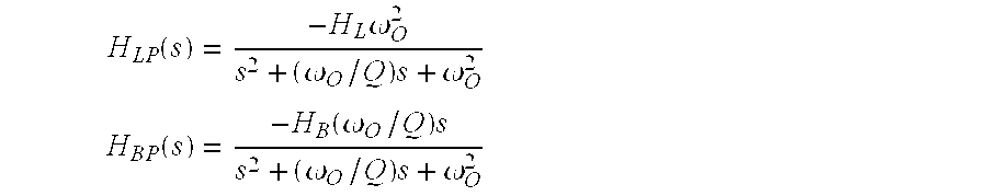
- H LP ⁇ ( s ) - H L ⁇ ⁇ O 2 s 2 + ( ⁇ O / Q ) ⁇ s + ⁇ O 2
- H BP ⁇ ( s ) - H B ⁇ ( ⁇ O / Q ) ⁇ s s 2 + ( ⁇ O / Q ) ⁇ s + ⁇ O 2
- H L ⁇ ⁇ ( low ⁇ ⁇ pass ⁇ ⁇ gain ) R 403
- R 401 H B ⁇ ⁇ (band-pass gain) R 405
- R 401 Q R 405 R 316 ⁇ R 403
- the center frequency, quality factor, and gains of filter 400 can be easily set by selecting particular values for resistors 401 , 403 , and 405 .
- no clocks, phase lock loops, digital signal processing, or tuning cycles are required to set these filter parameters.
- FIG. 5 shows two filter circuits 200 cascaded to advantageously construct a filter for higher order band-pass responses in accordance with the present invention.
- resistor 511 is simply coupled between the terminal 206 A (the band-pass output) and input terminal 204 B to cascade filter circuits 200 A and 200 B.
- filter 500 can be easily converted to a higher order low pass filter by simply coupling resistor 511 between terminals 202 A and 204 B instead of between terminals 206 A and 204 B.
- each filter circuit 200 is a virtual-ground summing point for a corresponding filter circuit 200 .
- the transfer functions of filter 400 are inverting (indicated by the minus sign).
- these phase inversions cancel, and the resulting filter 500 is a non-inverting filter.
- capacitor 601 and resistors 603 and 605 are coupled to filter circuit 200 in accordance with the present invention as shown in FIG. 6 .
- filter 200 easily changes from a low pass filter to a high pass filter by simply replacing resistor 401 with capacitor 601 .
- High pass frequency response V HP is provided at output terminal 206
- band-pass frequency response V BP is now provided at output terminal 202 .
- the band-pass transfer function of filter 600 is the same as the band-pass transfer function of filter 400 .
- C INTERNAL is the internal capacitance of filter 200 , which in the embodiments of filter circuit 200 and integrator 300 shown respectively in FIGS. 2 and 3 is
- resistor 401 With capacitor 601 affects only the gains. Thus, if resistors 603 and 605 are respectively equal to resistors 403 and 405 , the center frequencies and quality factors of filters 600 and 400 are equal.
- filter circuit 600 can be similarly cascaded as filter circuit 500 , except that resistors 501 and 511 are replaced with capacitors.
- FIG. 7 shows an exemplary embodiment of a configurable operational filter constructed with a plurality of filter circuits 200 in accordance with the present invention.
- Configurable filter 700 is preferably fabricated as an integrated circuit chip.
- configurable filter 700 can be alternatively constructed as a discrete component device.
- Configurable filter 700 includes filter circuits 200 A-D having input terminals 704 A-D and output terminals 702 A- D and 706 A-D, respectively. Filters of up to 12th order (i.e., twelve poles, another mathematical concept related to the transfer function) can be configured with configurable filter 700 . Note that while four filter circuits 200 are shown in FIG. 7 for illustrative purposes, other numbers of filter circuits 200 can be used to construct configurable filter 700 .
- Configurable filter 700 also includes voltage input terminal 722 for preferably receiving a positive voltage V+, voltage input terminal 724 for preferably receiving a negative voltage V ⁇ , and ground ⁇ terminal 726 for coupling to a DC or AC ground.
- voltage input terminals 722 and 724 are each bypassed with 0.1 ⁇ F capacitors to AC ground (as shown in FIGS. 10 - 13 ).
- Ground terminal 726 is coupled to an internal node of configurable filter 700 (not shown), which is the midpoint of a resistive voltage divider between voltage input terminals 722 and 724 . This results in a half-supply voltage that serves as an internal ground reference that advantageously permits configurable filter 700 to operate with single or dual supply voltages.
- ground terminal 726 is coupled to an AC or DC ground.
- voltage input terminal 724 (V ⁇ ) is coupled to system ground (the ground of the system using configurable filter 700 ).
- Ground terminal 726 is bypassed with at least a 0.1 ⁇ F capacitor to the system ground at voltage input terminal 724 (V ⁇ ).
- the internal ground reference establishes a reference voltage for the input and output signals in single supply operation.
- Configurable filter 700 preferably includes shutdown terminal 728 and shutdown circuitry 730 .
- Shutdown circuitry 730 is coupled to shutdown terminal 728 , voltage terminals 722 and 724 , and filter circuits 200 A-D. (For clarity, these connections are not shown in FIG. 7; furthermore, because shutdown circuitry 730 can be implemented by persons of ordinary skill in the art in accordance with the following description, shutdown circuitry 730 is not shown).
- Shutdown circuitry 730 drives configurable filter 700 into a shutdown state when shutdown terminal 728 is not receiving a logical 0 signal.
- shutdown circuitry 730 if shutdown terminal 728 receives a logical 1 signal, or is left open-circuited, shutdown circuitry 730 generates two disable signals OFF and OFFB that disable bias generator 732 and filter circuits 200 A-D. This causes ground terminal 726 and output terminals 702 A-D and 706 A-D to enter a high impedance state.
- a small pull-up current source at shutdown terminal 728 defaults configurable filter 700 to the shutdown state when shutdown terminal 728 is left open-circuited.
- Configurable filter 700 also preferably includes bias generator 732 , which biases filter circuits 200 A-D (for clarity, connections to and from bias generator 732 are not shown in FIG. 7 ).
- FIG. 8 shows an exemplary embodiment of bias generator 732 in accordance with the present invention.
- Bias generator 800 preferably includes a 5-bit programmable binary resistor array 840 to control the supply current of configurable filter 700 .
- Resistor array 840 adjusts for process variations and advantageously permits fabrication of lower power versions of configurable filter 700 .
- Resistor array 840 includes weighted resistors 841 - 846 and fuses 847 - 851 .
- Resistors 841 - 846 are preferable weighted as follows: resistor 842 is 2 ⁇ resistor 843 , resistor 843 is 2 resistor 844 , resistor 844 is 2 resistor 845 , and resistor 845 is 2 resistor 846 .
- Fuses 847 - 851 are preferably laser-fusible.
- Bias generator 800 also includes PMOS transistor 852 , which is preferably a long channel device that preferably provides a few microamperes of startup current to enable bias generator 800 to be DC self-starting under all conditions.
- Bias generator 800 further includes PMOS transistors 853 - 857 and 859 - 862 ; NPN transistors 863 , 864 , and 868 ; NMOS transistors 865 - 867 ; and capacitor 858 .
- Output nodes 869 - 872 are respectively coupled to filter circuits 200 A-D, and outputs OUT 0 - 3 respectively supply bias current to filter circuits 200 A-D.
- Signals OFFB and OFF received at respective nodes 873 , 874 are generated by shutdown circuitry 730 .
- FIG. 9 shows an exemplary embodiment of operational amplifier circuitry preferably used to construct inverter 314 and operational amplifiers 208 and 318 in accordance with the present invention.
- Operational amplifier (op-amp) circuit 900 includes output node 957 , inverting input node 958 , and non-inverting input node 959 .
- Nodes 960 and 961 respectively receive signals OFFB and OFF generated by shutdown circuitry 730 .
- Op amp circuit 900 is preferably an N-well CMOS circuit that advantageously does not use NMOS devices in the high gain portion of the signal path because of their inferior 1/f noise. Instead, N-well isolated NPN transistors 941 , 942 form a folded-cascode stage feeding high impedance PMOS current mirror 943 , 944 , 963 , 964 , 965 . Resistors 945 , 946 behave like current sources and are not a significant source of noise.
- PMOS transistor 947 is a level shift device that permits a convenient DC level at the first stage output (the collector of NPN transistor 942 ), and NPN transistor 948 is a clamp for rapid overload recovery driven by signal BIAS 1 .
- Signals BIAS 1 and BIAS 2 are outputs of circuitry described in commonly-owned U.S. patent application Ser. No. 09/113,618, filed Jul. 10, 1998, which is hereby incorporated by reference herein in its entirety.
- the output stage includes PMOS transistors 949 and 951 and NMOS transistors 950 , 952 , and 953 .
- NMOS transistor 950 and PMOS transistor 951 operate together as a composite NMOS device whose source voltage is set by signal BIAS 2 on the gate of PMOS transistor 951 , and whose equivalent “k” or g m (transconductance) parameter relates directly to those of NMOS transistor 950 and PMOS transistor 951 .
- NMOS transistors 952 , 953 form a 1:8 current mirror that draws the resulting drain current and combines it with that of PMOS transistor 949 in proper polarity.
- Signal BIAS 2 drives the gate of PMOS transistor 951 such that PMOS transistor 949 and NMOS transistor 950 operate with the same quiescent gate voltage.
- This open loop linear output stage prevents additional distortion at signal frequencies, where the overall loop gain is reduced.
- the output stage operates in class-A push-pull until the load current exceeds its quiescent current in either direction, and then the output stage makes a smooth symmetrical transition to class-AB with higher efficiency.
- Filter circuit 200 can therefore be programmed for lower current operation at a cost of increased distortion.
- op amp circuit 900 At the input stage of op amp circuit 900 , a tradeoff exists between distortion and noise. With a unity gain frequency ⁇ U and a given input-pair current source 954 , sizing input PMOS transistors 955 , 956 affects distortion and noise in opposite directions. (A high ratio of op amp slew rate to signal slew rate reduces distortion. Slew rate is a time rate of change of, for example, an output voltage under specified conditions.) Preferably, noise is favored in this tradeoff, because noise is the limiting factor in the dynamic range of signals that the filter can process.
- FIGS. 10-13 show exemplary embodiments of several types of active-RC filters constructed with configurable filter 700 in accordance with the present invention (for clarity, shutdown circuitry 730 and bias ,generator 732 are not shown in FIGS. 10 - 13 ).
- FIG. 10 shows an exemplary embodiment of a dual 4th order 100 k Hz Butterworth low pass filter 1000 constructed with configurable filter 700 .
- a Butterworth filter provides a maximally-flat passband frequency response.
- Each half of filter 1000 provides a unity-passband-gain low pass response.
- the positive voltage V+ is preferably about 5 volts and the negative voltage V ⁇ is preferably about ⁇ 5 volts.
- the circuit elements of filter 1000 are preferably about as follows:
- resistor 1001 A 10 k ohms
- resistor 1005 A 5.62 k ohms
- resistor 1003 A 10 k ohms
- resistor 1001 B 10 k ohms
- resistor 1005 B 13 k ohms
- resistor 1003 B 10 k ohms
- resistor 1001 C 10 k ohms
- resistor 1005 C 5.62 k ohms
- resistor 1003 C 10 k ohms
- resistor 1001 D 10 k ohms
- resistor 1005 D 13 k ohms
- resistor 1003 D 10 k ohms
- FIG. 11 shows an exemplary embodiment of an 8th order 100 k Hz low pass elliptic filter 1100 constructed with configurable filter 700 .
- Filter 1100 includes additional capacitors 1111 A and 1111 C in the input path, and sums these parallel resistor-capacitor paths at input terminals 704 A-D to produce two notches in the low pass stopband (the band of frequencies filtered out).
- the positive voltage V+ is preferably about 5 volts and the negative voltage V ⁇ is preferably about ⁇ 5 volts.
- the circuit elements of filter 1100 are preferably about as follows:
- resistor 1101 A 19.6 k ohms
- resistor 1105 A 13 k ohms
- resistor 1103 A 8.87 k ohms
- resistor 1101 B 8.06 k ohms
- resistor 1111 B 12.1 k ohms
- resistor 1105 B 8.87 k ohms
- resistor 1103 B 12.1 k ohms
- resistor 1101 C 69.8 k ohms
- resistor 1105 C 28 k ohms
- resistor 1103 C 8.87 k ohms
- resistor 1001 D 7.32 k ohms
- resistor 1111 D 17.8 k ohms
- resistor 1105 D 6.98 k ohms
- resistor 1103 D 17.8 k ohms
- FIG. 12 shows an exemplary embodiment of an 8th order Chebyshev high pass filter 1200 with about 0.05 dB ripple and a cutoff frequency of about 30 k Hz constructed with configurable filter 700 .
- Ripples are increases and decreases in gain within the passband (the range of frequencies allowed to pass through the filter).
- Each of the four cascaded filter circuits 200 A-D has an external capacitor in the input path (capacitors 1201 A-D).
- Resistors 1203 A-D and 1205 A-D set the respective center frequency and quality factor of filter circuits 200 A-D.
- the positive voltage V+ is preferably about 5 volts and the negative voltage V ⁇ is preferably about ⁇ 5 volts.
- the circuit elements of filter 1200 are preferably about as follows:
- resistor 1205 A 10.2 k ohms
- resistor 1203 A 35.7 k ohms
- resistor 1205 B 22.1 k ohms
- resistor 1203 B 66.5 k ohms
- resistor 1205 C 54.9 k ohms
- resistor 1203 C 107 k ohms
- resistor 1205 D 98.9 k ohms
- resistor 1203 D 127 k ohms
- FIG. 13 shows an exemplary embodiment of quadruple 3rd order 100 k Hz Butterworth low pass filter 1300 constructed with configurable filter 700 .
- Filter 1300 illustrates the flexibility of the virtual-ground inputs by permitting an extra, independent real pole to be added by replacing the input resistor (e.g., resistor 401 of FIG. 4) with an R-C-R “T” network.
- the input resistor e.g., resistor 401 of FIG. 4
- R-C-R “T” network As shown in FIG. 13, the input resistor is split into two parts (resistors 1301 A-D and 1321 A-D). This parallel combination forms a 100 k Hz real pole (for the values shown below) with external capacitors 1311 A-D.
- four such 3rd order Butterworth low pass filters can be constructed with configurable filter 700 for a total of twelve poles.
- the same technique can advantageously add additional real poles to other filter configurations as well, such as, for example, modifying dual 4th order low pass filter 1000 to produce a dual 5th order or dual 6th order filter.
- the positive voltage V+ of filter 1300 is preferably about 5 volts and the negative voltage V ⁇ is preferably about ⁇ 5 volts.
- the circuit elements are preferably about as follows:
- resistor 1301 A 6.19 k ohms
- resistor 1321 A 3.83 k ohms
- resistor 1305 A 10 k ohms
- resistor 1303 A 10 k ohms
- resistor 1301 B 6.19 k ohms
- resistor 1321 B 3.83 k ohms
- resistor 1305 B 10 k ohms
- resistor 1303 B 10 k ohms
- resistor 1301 C 6.19 k ohms
- resistor 1321 C 3.83 k ohms
- resistor 1305 C 10 k ohms
- resistor 1303 C 10 k ohms
- resistor 1301 D 6.19 k ohms
- resistor 1321 D 3.83 k ohms
- resistor 1305 D 10 k ohms
- resistor 1303 D 10 k ohms
- an exemplary embodiment of a quadruple 3rd order high pass filter can be constructed with filter 1300 simply by replacing resistors 1301 A-D and 1321 A-D with capacitors, and by replacing capacitors 1311 A-D with resistors.
- the high pass outputs are then provided at terminals 706 A-D of configurable filter 700 .
- Filter circuit 200 and configurable filter 700 can also be used to construct notch, or band-reject, filters. Notch filters ideally have zero signal gain at a notch frequency f N .
- H N is set by circuit component values as described further below.
- the center frequency f O and quality factor Q are set as described above with respect to FIGS. 3, 4 , and 6 .
- the gain is H N ⁇ ⁇ f N 2 f O 2
- Notch filters can be constructed by adding a signal to a filtered replica of itself having equal gain and a 180° phase difference at the desired notch frequency f N . The two signals then cancel each other out at f N .
- the “notch depth” i.e., the degree of signal cancellation
- the “notch depth” will be infinite to the extent that the two signals have matching gains. In other words, if the gains match and the signals are 180° out of phase at frequency f N , the gain of the summed signals at f N is zero.
- FIG. 14A shows notch filter 1400 constructed in accordance with the present invention.
- op amp 1410 and resistor 1415 serve as a virtual-ground summing circuit.
- the notch produced by filter 1400 equals the center frequency of the filter and the notch transfer function parameters are:
- capacitor 1402 advantageously contributes phase lead, which increases the notch frequency above the center frequency of filter circuit 200 A.
- Notch filter 1400 is typically most useful as a stopband notch in a low pass filter or as an upper stopband notch in a band-pass filter.
- Resistors 1411 and 1417 simply replace the input resistor of either a low pass or resistor-input band-pass section of a cascaded filter circuit 200 (e.g., resistor 511 of filter circuit 200 B of FIG. 5 ).
- FIG. 14B shows high order cascaded notch filter 1450 constructed with filter circuit 200 in accordance with the present invention.
- Notch filter 1450 provides a two-notch 8-pole low pass response V N . The frequency of the two notches are each greater than the center frequency.
- Notch filter 1450 includes filter circuits 200 A-D, capacitors 1402 and 1452 , and resistors 1401 , 1403 , 1405 , 1411 , 1413 , 1415 , 1417 , 1451 , 1453 , 1455 , 1461 , 1463 , 1465 , and 1467 , coupled as shown.
- Filter circuits 200 A and 200 C each create a notch
- filter circuits 200 B and 200 D each function as a summing circuit.
- FIG. 17 shows notch filter 1700 constructed in accordance with the present invention.
- notch filter 1700 By summing the inverted low pass output signal at output terminal 202 with input signal V IN at op amp 1710 as shown, notch filter 1700 produces a notch at a frequency f N ⁇ f O . If the value of capacitor 1702 is zero, notch frequency fN is zero (i.e., the notch occurs when the input signal is DC).
- capacitor 1702 If the value of capacitor 1702 is not zero, capacitor 1702 provides phase lead that shifts the notch frequency up from zero, resulting in a low frequency notch with a high pass response, as shown in the notch frequency response of FIG. 18 .
- Notch filter 1700 is typically most useful as a lower stopband notch in a band-pass filter.
- Resistors 1711 and 1717 simply replace the input resistor of a cascaded filter circuit 200 (e.g., resistor 511 of filter circuit 200 B of FIG. 5 ).
- FIG. 19 shows notch filter 1900 constructed in accordance with the present invention.
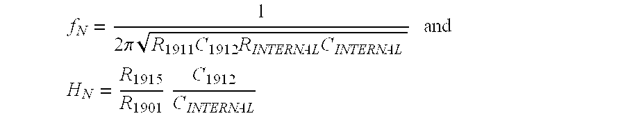
- Notch filter 1900 provides notches by summing the low pass and band-pass output signals, which are 90° out of phase, through resistor 1911 and capacitor 1912 , respectively, at op amp 1910 as shown.
- the low pass output signal is provided at output terminal 202 and the band-pass output signal is provided at output terminal 206 .
- Capacitor 1912 provides another 90° phase shift to the band-pass output signal. This results in a wideband 180° phase difference.
- the amplitude ratio between currents I R and I C is frequency-dependent. At the frequency where I R and I C have equal magnitude, Io becomes zero and a notch occurs.
- Notch filter 1900 can therefore provide deep notches (i.e., substantially complete signal cancellation) independent of these element/component relationships.
- variations in the values of resistor 1911 or capacitor 1912 vary the notch frequency, not the degree of signal cancellation.
- the notch frequency is independent of the center frequency. The notch frequency can thus be equal to, higher than, or lower than the center frequency without reconfiguring the circuit elements as is necessary to go to and from notch filters 1400 and 1700 when a notch frequency on the other side of the center frequency is desired.
- Notch filter 2000 includes filter circuits 200 A and 200 B, capacitors 1912 and 2012 , and resistors 1901 , 1903 , 1905 , 1911 , 1915 , 2003 , and 2011 .
- Node 2014 can be coupled to a summing circuit (e.g., op amp 1910 and resistor 1915 ) to provide a two-notch 4-pole gain response where one notch is created by filter circuit 200 A and another is created by filter circuit 200 B.
- a summing circuit e.g., op amp 1910 and resistor 1915
- node 2014 can be coupled to another filter circuit 200 to obtain higher order responses.
- notch filter 2000 could provide any of the following responses: if filter circuit 200 C functioned as a summing circuit, then a two-notch 6-pole low pass or band-pass gain response is provided at output terminal 202 C or 206 C, respectively. If filter circuit 200 C were configured as filter circuit 200 B with node 2014 C (not shown) coupled to a summing circuit, then notch filter 2000 would provide a three-notch 6-pole gain response where filter circuits 200 A-C each create a notch. Notch filter 2000 can be accordingly cascaded further.
Abstract
Description


Claims (26)
Priority Applications (1)
| Application Number | Priority Date | Filing Date | Title |
|---|---|---|---|
| US09/305,132 US6271720B1 (en) | 1998-09-02 | 1999-05-04 | Operational filter building block |
Applications Claiming Priority (2)
| Application Number | Priority Date | Filing Date | Title |
|---|---|---|---|
| US09/145,536 US6271719B1 (en) | 1998-09-02 | 1998-09-02 | Operational filter building block |
| US09/305,132 US6271720B1 (en) | 1998-09-02 | 1999-05-04 | Operational filter building block |
Related Parent Applications (1)
| Application Number | Title | Priority Date | Filing Date |
|---|---|---|---|
| US09/145,536 Continuation-In-Part US6271719B1 (en) | 1998-09-02 | 1998-09-02 | Operational filter building block |
Publications (1)
| Publication Number | Publication Date |
|---|---|
| US6271720B1 true US6271720B1 (en) | 2001-08-07 |
Family
ID=46256424
Family Applications (1)
| Application Number | Title | Priority Date | Filing Date |
|---|---|---|---|
| US09/305,132 Expired - Lifetime US6271720B1 (en) | 1998-09-02 | 1999-05-04 | Operational filter building block |
Country Status (1)
| Country | Link |
|---|---|
| US (1) | US6271720B1 (en) |
Cited By (30)
| Publication number | Priority date | Publication date | Assignee | Title |
|---|---|---|---|---|
| US6445735B1 (en) * | 1999-02-08 | 2002-09-03 | Visteon Global Technologies, Inc. | Switched bandwidth digital filters with reduced transients during switching |
| WO2003003059A2 (en) * | 2001-06-29 | 2003-01-09 | Corning Incorporated | Optical system that improves spectrally distorted signals |
| US20040052217A1 (en) * | 2002-09-16 | 2004-03-18 | Anghel Cristian E. | Position sensor emulator for a synchronous motor/generator |
| US20070076782A1 (en) * | 2005-09-30 | 2007-04-05 | Freescale Semiconductor, Inc. | Method and system for controlling a notching mechanism |
| US20080111714A1 (en) * | 2006-11-14 | 2008-05-15 | Viktor Kremin | Capacitance to code converter with sigma-delta modulator |
| US20080136792A1 (en) * | 2006-12-07 | 2008-06-12 | Tao Peng | Preventing unintentional activation of a touch-sensor button caused by a presence of conductive liquid on the touch-sensor button |
| US20080196945A1 (en) * | 2007-02-21 | 2008-08-21 | Jason Konstas | Preventing unintentional activation of a sensor element of a sensing device |
| US20080204166A1 (en) * | 2007-02-22 | 2008-08-28 | Shafer Steven K | Dual Bandstop Filter With Enhanced Upper Passband Response |
| US7616705B1 (en) * | 2000-07-27 | 2009-11-10 | Sirf Technology Holdings, Inc. | Monolithic GPS RF front end integrated circuit |
| US20100254794A1 (en) * | 2001-08-01 | 2010-10-07 | Top Tier, Inc. | Palletizer Puller Bar |
| US8058937B2 (en) | 2007-01-30 | 2011-11-15 | Cypress Semiconductor Corporation | Setting a discharge rate and a charge rate of a relaxation oscillator circuit |
| US20110316519A1 (en) * | 2010-06-25 | 2011-12-29 | David Schie | Load Switch |
| US8089288B1 (en) | 2006-11-16 | 2012-01-03 | Cypress Semiconductor Corporation | Charge accumulation capacitance sensor with linear transfer characteristic |
| US8089289B1 (en) | 2007-07-03 | 2012-01-03 | Cypress Semiconductor Corporation | Capacitive field sensor with sigma-delta modulator |
| US8169238B1 (en) | 2007-07-03 | 2012-05-01 | Cypress Semiconductor Corporation | Capacitance to frequency converter |
| US8248084B2 (en) | 2006-03-31 | 2012-08-21 | Cypress Semiconductor Corporation | Touch detection techniques for capacitive touch sense systems |
| US8321174B1 (en) | 2008-09-26 | 2012-11-27 | Cypress Semiconductor Corporation | System and method to measure capacitance of capacitive sensor array |
| US8358142B2 (en) | 2008-02-27 | 2013-01-22 | Cypress Semiconductor Corporation | Methods and circuits for measuring mutual and self capacitance |
| US8487639B1 (en) | 2008-11-21 | 2013-07-16 | Cypress Semiconductor Corporation | Receive demodulator for capacitive sensing |
| US8493351B2 (en) | 2006-03-30 | 2013-07-23 | Cypress Semiconductor Corporation | Apparatus and method for reducing average scan rate to detect a conductive object on a sensing device |
| US8525798B2 (en) | 2008-01-28 | 2013-09-03 | Cypress Semiconductor Corporation | Touch sensing |
| US8570053B1 (en) | 2007-07-03 | 2013-10-29 | Cypress Semiconductor Corporation | Capacitive field sensor with sigma-delta modulator |
| US8570052B1 (en) | 2008-02-27 | 2013-10-29 | Cypress Semiconductor Corporation | Methods and circuits for measuring mutual and self capacitance |
| US8866500B2 (en) | 2009-03-26 | 2014-10-21 | Cypress Semiconductor Corporation | Multi-functional capacitance sensing circuit with a current conveyor |
| US8976124B1 (en) | 2007-05-07 | 2015-03-10 | Cypress Semiconductor Corporation | Reducing sleep current in a capacitance sensing system |
| US20150112621A1 (en) * | 2012-06-01 | 2015-04-23 | Mitsubishi Electric Corporation | Voltage detection device for transforming apparatus |
| US9104273B1 (en) | 2008-02-29 | 2015-08-11 | Cypress Semiconductor Corporation | Multi-touch sensing method |
| US9268441B2 (en) | 2011-04-05 | 2016-02-23 | Parade Technologies, Ltd. | Active integrator for a capacitive sense array |
| US9417728B2 (en) | 2009-07-28 | 2016-08-16 | Parade Technologies, Ltd. | Predictive touch surface scanning |
| US9500686B1 (en) | 2007-06-29 | 2016-11-22 | Cypress Semiconductor Corporation | Capacitance measurement system and methods |
Citations (2)
| Publication number | Priority date | Publication date | Assignee | Title |
|---|---|---|---|---|
| US4417214A (en) | 1981-04-13 | 1983-11-22 | National Semiconductor Corporation | Monolithic IC general purpose active filter |
| US4453132A (en) * | 1982-04-21 | 1984-06-05 | Motorola, Inc. | Active filter |
-
1999
- 1999-05-04 US US09/305,132 patent/US6271720B1/en not_active Expired - Lifetime
Patent Citations (2)
| Publication number | Priority date | Publication date | Assignee | Title |
|---|---|---|---|---|
| US4417214A (en) | 1981-04-13 | 1983-11-22 | National Semiconductor Corporation | Monolithic IC general purpose active filter |
| US4453132A (en) * | 1982-04-21 | 1984-06-05 | Motorola, Inc. | Active filter |
Non-Patent Citations (2)
| Title |
|---|
| Arthur B. Williams, Electronic Filter Design Handbook, pp. 6-28 to 6-31, McGraw-Hill, 1981. |
| Harry Y-F. Lam, Analog and Digital Filters, Design and Realization, pp. 401-411, Prentice-Hall, 1979. |
Cited By (53)
| Publication number | Priority date | Publication date | Assignee | Title |
|---|---|---|---|---|
| US6445735B1 (en) * | 1999-02-08 | 2002-09-03 | Visteon Global Technologies, Inc. | Switched bandwidth digital filters with reduced transients during switching |
| US7616705B1 (en) * | 2000-07-27 | 2009-11-10 | Sirf Technology Holdings, Inc. | Monolithic GPS RF front end integrated circuit |
| WO2003003059A2 (en) * | 2001-06-29 | 2003-01-09 | Corning Incorporated | Optical system that improves spectrally distorted signals |
| WO2003003059A3 (en) * | 2001-06-29 | 2003-05-01 | Corning Inc | Optical system that improves spectrally distorted signals |
| US20100254794A1 (en) * | 2001-08-01 | 2010-10-07 | Top Tier, Inc. | Palletizer Puller Bar |
| US20040052217A1 (en) * | 2002-09-16 | 2004-03-18 | Anghel Cristian E. | Position sensor emulator for a synchronous motor/generator |
| US6809496B2 (en) * | 2002-09-16 | 2004-10-26 | Honeywell International Inc. | Position sensor emulator for a synchronous motor/generator |
| US20070076782A1 (en) * | 2005-09-30 | 2007-04-05 | Freescale Semiconductor, Inc. | Method and system for controlling a notching mechanism |
| US7502410B2 (en) * | 2005-09-30 | 2009-03-10 | Freescale Semiconductor, Inc. | Method and system for controlling a notching mechanism |
| US8493351B2 (en) | 2006-03-30 | 2013-07-23 | Cypress Semiconductor Corporation | Apparatus and method for reducing average scan rate to detect a conductive object on a sensing device |
| US9152284B1 (en) | 2006-03-30 | 2015-10-06 | Cypress Semiconductor Corporation | Apparatus and method for reducing average scan rate to detect a conductive object on a sensing device |
| US8248084B2 (en) | 2006-03-31 | 2012-08-21 | Cypress Semiconductor Corporation | Touch detection techniques for capacitive touch sense systems |
| US9494627B1 (en) | 2006-03-31 | 2016-11-15 | Monterey Research, Llc | Touch detection techniques for capacitive touch sense systems |
| US9154160B2 (en) | 2006-11-14 | 2015-10-06 | Cypress Semiconductor Corporation | Capacitance to code converter with sigma-delta modulator |
| US8547114B2 (en) | 2006-11-14 | 2013-10-01 | Cypress Semiconductor Corporation | Capacitance to code converter with sigma-delta modulator |
| US20080111714A1 (en) * | 2006-11-14 | 2008-05-15 | Viktor Kremin | Capacitance to code converter with sigma-delta modulator |
| US9166621B2 (en) | 2006-11-14 | 2015-10-20 | Cypress Semiconductor Corporation | Capacitance to code converter with sigma-delta modulator |
| US8089288B1 (en) | 2006-11-16 | 2012-01-03 | Cypress Semiconductor Corporation | Charge accumulation capacitance sensor with linear transfer characteristic |
| US20080136792A1 (en) * | 2006-12-07 | 2008-06-12 | Tao Peng | Preventing unintentional activation of a touch-sensor button caused by a presence of conductive liquid on the touch-sensor button |
| US8902172B2 (en) | 2006-12-07 | 2014-12-02 | Cypress Semiconductor Corporation | Preventing unintentional activation of a touch-sensor button caused by a presence of conductive liquid on the touch-sensor button |
| US8058937B2 (en) | 2007-01-30 | 2011-11-15 | Cypress Semiconductor Corporation | Setting a discharge rate and a charge rate of a relaxation oscillator circuit |
| US20080196945A1 (en) * | 2007-02-21 | 2008-08-21 | Jason Konstas | Preventing unintentional activation of a sensor element of a sensing device |
| US7592882B2 (en) | 2007-02-22 | 2009-09-22 | John Mezzalingua Associates, Inc. | Dual bandstop filter with enhanced upper passband response |
| US20080204166A1 (en) * | 2007-02-22 | 2008-08-28 | Shafer Steven K | Dual Bandstop Filter With Enhanced Upper Passband Response |
| US8976124B1 (en) | 2007-05-07 | 2015-03-10 | Cypress Semiconductor Corporation | Reducing sleep current in a capacitance sensing system |
| US10788937B2 (en) | 2007-05-07 | 2020-09-29 | Cypress Semiconductor Corporation | Reducing sleep current in a capacitance sensing system |
| US9500686B1 (en) | 2007-06-29 | 2016-11-22 | Cypress Semiconductor Corporation | Capacitance measurement system and methods |
| US8536902B1 (en) * | 2007-07-03 | 2013-09-17 | Cypress Semiconductor Corporation | Capacitance to frequency converter |
| US8570053B1 (en) | 2007-07-03 | 2013-10-29 | Cypress Semiconductor Corporation | Capacitive field sensor with sigma-delta modulator |
| US8169238B1 (en) | 2007-07-03 | 2012-05-01 | Cypress Semiconductor Corporation | Capacitance to frequency converter |
| US8089289B1 (en) | 2007-07-03 | 2012-01-03 | Cypress Semiconductor Corporation | Capacitive field sensor with sigma-delta modulator |
| US8525798B2 (en) | 2008-01-28 | 2013-09-03 | Cypress Semiconductor Corporation | Touch sensing |
| US9760192B2 (en) | 2008-01-28 | 2017-09-12 | Cypress Semiconductor Corporation | Touch sensing |
| US8358142B2 (en) | 2008-02-27 | 2013-01-22 | Cypress Semiconductor Corporation | Methods and circuits for measuring mutual and self capacitance |
| US8570052B1 (en) | 2008-02-27 | 2013-10-29 | Cypress Semiconductor Corporation | Methods and circuits for measuring mutual and self capacitance |
| US8692563B1 (en) | 2008-02-27 | 2014-04-08 | Cypress Semiconductor Corporation | Methods and circuits for measuring mutual and self capacitance |
| US9494628B1 (en) | 2008-02-27 | 2016-11-15 | Parade Technologies, Ltd. | Methods and circuits for measuring mutual and self capacitance |
| US9423427B2 (en) | 2008-02-27 | 2016-08-23 | Parade Technologies, Ltd. | Methods and circuits for measuring mutual and self capacitance |
| US9104273B1 (en) | 2008-02-29 | 2015-08-11 | Cypress Semiconductor Corporation | Multi-touch sensing method |
| US8321174B1 (en) | 2008-09-26 | 2012-11-27 | Cypress Semiconductor Corporation | System and method to measure capacitance of capacitive sensor array |
| US10386969B1 (en) | 2008-09-26 | 2019-08-20 | Cypress Semiconductor Corporation | System and method to measure capacitance of capacitive sensor array |
| US11029795B2 (en) | 2008-09-26 | 2021-06-08 | Cypress Semiconductor Corporation | System and method to measure capacitance of capacitive sensor array |
| US8575947B1 (en) | 2008-11-21 | 2013-11-05 | Cypress Semiconductor Corporation | Receive demodulator for capacitive sensing |
| US8487639B1 (en) | 2008-11-21 | 2013-07-16 | Cypress Semiconductor Corporation | Receive demodulator for capacitive sensing |
| US8866500B2 (en) | 2009-03-26 | 2014-10-21 | Cypress Semiconductor Corporation | Multi-functional capacitance sensing circuit with a current conveyor |
| US9442146B2 (en) | 2009-03-26 | 2016-09-13 | Parade Technologies, Ltd. | Multi-mode capacitive sensing device and method with current conveyor |
| US9417728B2 (en) | 2009-07-28 | 2016-08-16 | Parade Technologies, Ltd. | Predictive touch surface scanning |
| US8378658B2 (en) * | 2010-06-25 | 2013-02-19 | Micrel, Inc. | Load swtch for removing high frequency ripple, noise and/or spikes while providing power to subsystems |
| CN102394615A (en) * | 2010-06-25 | 2012-03-28 | 迈瑞公司 | Load switch |
| US20110316519A1 (en) * | 2010-06-25 | 2011-12-29 | David Schie | Load Switch |
| US9268441B2 (en) | 2011-04-05 | 2016-02-23 | Parade Technologies, Ltd. | Active integrator for a capacitive sense array |
| US10338102B2 (en) * | 2012-06-01 | 2019-07-02 | Mitsubishi Electric Corporation | Voltage detection device for transforming apparatus |
| US20150112621A1 (en) * | 2012-06-01 | 2015-04-23 | Mitsubishi Electric Corporation | Voltage detection device for transforming apparatus |
Similar Documents
| Publication | Publication Date | Title |
|---|---|---|
| US6271720B1 (en) | Operational filter building block | |
| US6271719B1 (en) | Operational filter building block | |
| Banu et al. | An elliptic continuous-time CMOS filter with on-chip automatic tuning | |
| US6344773B1 (en) | Flexible monolithic continuous-time analog low-pass filter with minimal circuitry | |
| US6476676B1 (en) | Semiconductor integrated circuit | |
| KR19980064159A (en) | Filter circuit | |
| EP1755218B1 (en) | Tunable resonator for use in active-RC continuous-time filters | |
| Anurag et al. | OTRA based shadow filters | |
| Arora et al. | Fully integrable/cascadable CM universal filter and CM quadrature oscillator using VDCC and only grounded passive elements | |
| Kumngern et al. | Current-mode universal filter and quadrature oscillator using current controlled current follower transconductance amplifiers | |
| US4147997A (en) | Active filters utilizing networks of resistors and negative impedance converters | |
| Frey et al. | An adaptive analog notch filter using log filtering | |
| Nonthaputha et al. | Programmable universal filters using current conveyor transconductance amplifiers | |
| EP1737128B1 (en) | Impedance conversion circuit and integrated circuit including the same | |
| US20060053193A1 (en) | Complex multiple feedback filter | |
| JP2790278B2 (en) | Delay circuit | |
| US6255905B1 (en) | Active filter circuit having a T-network input arrangement that provides a high input impedance | |
| US4001735A (en) | Single amplifier immittance network | |
| Sagbas et al. | Voltage-mode three-input single-output multifunction filters employing minimum number of components | |
| Lakys et al. | Cognitive and encrypted communications, part 2: A new approach to active frequency-agile filters and validation results for an agile bandpass yopology in SiGe-BiCMOS | |
| Lata et al. | Cascadable current-mode biquads | |
| US6549066B1 (en) | Efficient implementation of a complex filter with on chip resistor tuning | |
| Senani et al. | Second generation controlled current conveyors (CCCII) and their applications | |
| JP2539301B2 (en) | Polarized Leapfrog Filter | |
| Langhammer et al. | Dual-mode multifunctional reconnection-less reconfigurable filter |
Legal Events
| Date | Code | Title | Description |
|---|---|---|---|
| AS | Assignment |
Owner name: LINEAR TECHNOLOGY CORPORATION, CALIFORNIA Free format text: ASSIGNMENT OF ASSIGNORS INTEREST;ASSIGNOR:SEVASTOPOULOS, NELLO GEORGE;REEL/FRAME:010224/0392 Effective date: 19990729 |
|
| STCF | Information on status: patent grant |
Free format text: PATENTED CASE |
|
| CC | Certificate of correction | ||
| FPAY | Fee payment |
Year of fee payment: 4 |
|
| FEPP | Fee payment procedure |
Free format text: PAYOR NUMBER ASSIGNED (ORIGINAL EVENT CODE: ASPN); ENTITY STATUS OF PATENT OWNER: LARGE ENTITY |
|
| FPAY | Fee payment |
Year of fee payment: 8 |
|
| REMI | Maintenance fee reminder mailed | ||
| FPAY | Fee payment |
Year of fee payment: 12 |
|
| AS | Assignment |
Owner name: ANALOG DEVICES INTERNATIONAL UNLIMITED COMPANY, IRELAND Free format text: CHANGE OF NAME;ASSIGNOR:LINEAR TECHNOLOGY LLC;REEL/FRAME:057423/0205 Effective date: 20181105 Owner name: LINEAR TECHNOLOGY LLC, CALIFORNIA Free format text: CHANGE OF NAME;ASSIGNOR:LINEAR TECHNOLOGY CORPORATION;REEL/FRAME:057421/0714 Effective date: 20170502 |