US6261889B1 - Manufacturing method of semiconductor device - Google Patents

Manufacturing method of semiconductor device Download PDF

Info

Publication number
US6261889B1
US6261889B1 US09/525,904 US52590400A US6261889B1 US 6261889 B1 US6261889 B1 US 6261889B1 US 52590400 A US52590400 A US 52590400A US 6261889 B1 US6261889 B1 US 6261889B1
Authority
US
United States
Prior art keywords
fluorine
manufacturing
semiconductor device
heat treatment
gate electrode
Prior art date
Legal status (The legal status is an assumption and is not a legal conclusion. Google has not performed a legal analysis and makes no representation as to the accuracy of the status listed.)
Expired - Fee Related
Application number
US09/525,904
Inventor
Atsuki Ono
Current Assignee (The listed assignees may be inaccurate. Google has not performed a legal analysis and makes no representation or warranty as to the accuracy of the list.)
NEC Electronics Corp
Original Assignee
NEC Corp
Priority date (The priority date is an assumption and is not a legal conclusion. Google has not performed a legal analysis and makes no representation as to the accuracy of the date listed.)
Filing date
Publication date
Application filed by NEC Corp filed Critical NEC Corp
Assigned to NEC CORPORATION reassignment NEC CORPORATION ASSIGNMENT OF ASSIGNORS INTEREST (SEE DOCUMENT FOR DETAILS). Assignors: ONO, ATSUKI
Application granted granted Critical
Publication of US6261889B1 publication Critical patent/US6261889B1/en
Assigned to NEC ELECTRONICS CORPORATION reassignment NEC ELECTRONICS CORPORATION ASSIGNMENT OF ASSIGNORS INTEREST (SEE DOCUMENT FOR DETAILS). Assignors: NEC CORPORATION
Anticipated expiration legal-status Critical
Expired - Fee Related legal-status Critical Current

Links

Images

Classifications

    • HELECTRICITY
    • H01ELECTRIC ELEMENTS
    • H01LSEMICONDUCTOR DEVICES NOT COVERED BY CLASS H10
    • H01L21/00Processes or apparatus adapted for the manufacture or treatment of semiconductor or solid state devices or of parts thereof
    • H01L21/02Manufacture or treatment of semiconductor devices or of parts thereof
    • H01L21/04Manufacture or treatment of semiconductor devices or of parts thereof the devices having at least one potential-jump barrier or surface barrier, e.g. PN junction, depletion layer or carrier concentration layer
    • H01L21/18Manufacture or treatment of semiconductor devices or of parts thereof the devices having at least one potential-jump barrier or surface barrier, e.g. PN junction, depletion layer or carrier concentration layer the devices having semiconductor bodies comprising elements of Group IV of the Periodic System or AIIIBV compounds with or without impurities, e.g. doping materials
    • H01L21/26Bombardment with radiation
    • H01L21/263Bombardment with radiation with high-energy radiation
    • H01L21/265Bombardment with radiation with high-energy radiation producing ion implantation
    • H01L21/26506Bombardment with radiation with high-energy radiation producing ion implantation in group IV semiconductors
    • HELECTRICITY
    • H01ELECTRIC ELEMENTS
    • H01LSEMICONDUCTOR DEVICES NOT COVERED BY CLASS H10
    • H01L21/00Processes or apparatus adapted for the manufacture or treatment of semiconductor or solid state devices or of parts thereof
    • H01L21/70Manufacture or treatment of devices consisting of a plurality of solid state components formed in or on a common substrate or of parts thereof; Manufacture of integrated circuit devices or of parts thereof
    • H01L21/77Manufacture or treatment of devices consisting of a plurality of solid state components or integrated circuits formed in, or on, a common substrate
    • H01L21/78Manufacture or treatment of devices consisting of a plurality of solid state components or integrated circuits formed in, or on, a common substrate with subsequent division of the substrate into plural individual devices
    • H01L21/82Manufacture or treatment of devices consisting of a plurality of solid state components or integrated circuits formed in, or on, a common substrate with subsequent division of the substrate into plural individual devices to produce devices, e.g. integrated circuits, each consisting of a plurality of components
    • H01L21/822Manufacture or treatment of devices consisting of a plurality of solid state components or integrated circuits formed in, or on, a common substrate with subsequent division of the substrate into plural individual devices to produce devices, e.g. integrated circuits, each consisting of a plurality of components the substrate being a semiconductor, using silicon technology
    • H01L21/8232Field-effect technology
    • H01L21/8234MIS technology, i.e. integration processes of field effect transistors of the conductor-insulator-semiconductor type
    • H01L21/823437MIS technology, i.e. integration processes of field effect transistors of the conductor-insulator-semiconductor type with a particular manufacturing method of the gate conductors, e.g. particular materials, shapes
    • HELECTRICITY
    • H01ELECTRIC ELEMENTS
    • H01LSEMICONDUCTOR DEVICES NOT COVERED BY CLASS H10
    • H01L21/00Processes or apparatus adapted for the manufacture or treatment of semiconductor or solid state devices or of parts thereof
    • H01L21/02Manufacture or treatment of semiconductor devices or of parts thereof
    • H01L21/04Manufacture or treatment of semiconductor devices or of parts thereof the devices having at least one potential-jump barrier or surface barrier, e.g. PN junction, depletion layer or carrier concentration layer
    • H01L21/18Manufacture or treatment of semiconductor devices or of parts thereof the devices having at least one potential-jump barrier or surface barrier, e.g. PN junction, depletion layer or carrier concentration layer the devices having semiconductor bodies comprising elements of Group IV of the Periodic System or AIIIBV compounds with or without impurities, e.g. doping materials
    • H01L21/26Bombardment with radiation
    • H01L21/263Bombardment with radiation with high-energy radiation
    • H01L21/265Bombardment with radiation with high-energy radiation producing ion implantation
    • H01L21/2658Bombardment with radiation with high-energy radiation producing ion implantation of a molecular ion, e.g. decaborane
    • HELECTRICITY
    • H01ELECTRIC ELEMENTS
    • H01LSEMICONDUCTOR DEVICES NOT COVERED BY CLASS H10
    • H01L21/00Processes or apparatus adapted for the manufacture or treatment of semiconductor or solid state devices or of parts thereof
    • H01L21/02Manufacture or treatment of semiconductor devices or of parts thereof
    • H01L21/04Manufacture or treatment of semiconductor devices or of parts thereof the devices having at least one potential-jump barrier or surface barrier, e.g. PN junction, depletion layer or carrier concentration layer
    • H01L21/18Manufacture or treatment of semiconductor devices or of parts thereof the devices having at least one potential-jump barrier or surface barrier, e.g. PN junction, depletion layer or carrier concentration layer the devices having semiconductor bodies comprising elements of Group IV of the Periodic System or AIIIBV compounds with or without impurities, e.g. doping materials
    • H01L21/28Manufacture of electrodes on semiconductor bodies using processes or apparatus not provided for in groups H01L21/20 - H01L21/268
    • H01L21/28008Making conductor-insulator-semiconductor electrodes
    • H01L21/28017Making conductor-insulator-semiconductor electrodes the insulator being formed after the semiconductor body, the semiconductor being silicon
    • H01L21/28158Making the insulator
    • H01L21/28167Making the insulator on single crystalline silicon, e.g. using a liquid, i.e. chemical oxidation
    • H01L21/28176Making the insulator on single crystalline silicon, e.g. using a liquid, i.e. chemical oxidation with a treatment, e.g. annealing, after the formation of the definitive gate conductor
    • HELECTRICITY
    • H01ELECTRIC ELEMENTS
    • H01LSEMICONDUCTOR DEVICES NOT COVERED BY CLASS H10
    • H01L21/00Processes or apparatus adapted for the manufacture or treatment of semiconductor or solid state devices or of parts thereof
    • H01L21/70Manufacture or treatment of devices consisting of a plurality of solid state components formed in or on a common substrate or of parts thereof; Manufacture of integrated circuit devices or of parts thereof
    • H01L21/77Manufacture or treatment of devices consisting of a plurality of solid state components or integrated circuits formed in, or on, a common substrate
    • H01L21/78Manufacture or treatment of devices consisting of a plurality of solid state components or integrated circuits formed in, or on, a common substrate with subsequent division of the substrate into plural individual devices
    • H01L21/82Manufacture or treatment of devices consisting of a plurality of solid state components or integrated circuits formed in, or on, a common substrate with subsequent division of the substrate into plural individual devices to produce devices, e.g. integrated circuits, each consisting of a plurality of components
    • H01L21/822Manufacture or treatment of devices consisting of a plurality of solid state components or integrated circuits formed in, or on, a common substrate with subsequent division of the substrate into plural individual devices to produce devices, e.g. integrated circuits, each consisting of a plurality of components the substrate being a semiconductor, using silicon technology
    • H01L21/8232Field-effect technology
    • H01L21/8234MIS technology, i.e. integration processes of field effect transistors of the conductor-insulator-semiconductor type
    • H01L21/823418MIS technology, i.e. integration processes of field effect transistors of the conductor-insulator-semiconductor type with a particular manufacturing method of the source or drain structures, e.g. specific source or drain implants or silicided source or drain structures or raised source or drain structures
    • HELECTRICITY
    • H01ELECTRIC ELEMENTS
    • H01LSEMICONDUCTOR DEVICES NOT COVERED BY CLASS H10
    • H01L21/00Processes or apparatus adapted for the manufacture or treatment of semiconductor or solid state devices or of parts thereof
    • H01L21/70Manufacture or treatment of devices consisting of a plurality of solid state components formed in or on a common substrate or of parts thereof; Manufacture of integrated circuit devices or of parts thereof
    • H01L21/77Manufacture or treatment of devices consisting of a plurality of solid state components or integrated circuits formed in, or on, a common substrate
    • H01L21/78Manufacture or treatment of devices consisting of a plurality of solid state components or integrated circuits formed in, or on, a common substrate with subsequent division of the substrate into plural individual devices
    • H01L21/82Manufacture or treatment of devices consisting of a plurality of solid state components or integrated circuits formed in, or on, a common substrate with subsequent division of the substrate into plural individual devices to produce devices, e.g. integrated circuits, each consisting of a plurality of components
    • H01L21/822Manufacture or treatment of devices consisting of a plurality of solid state components or integrated circuits formed in, or on, a common substrate with subsequent division of the substrate into plural individual devices to produce devices, e.g. integrated circuits, each consisting of a plurality of components the substrate being a semiconductor, using silicon technology
    • H01L21/8232Field-effect technology
    • H01L21/8234MIS technology, i.e. integration processes of field effect transistors of the conductor-insulator-semiconductor type
    • H01L21/8238Complementary field-effect transistors, e.g. CMOS
    • H01L21/823807Complementary field-effect transistors, e.g. CMOS with a particular manufacturing method of the channel structures, e.g. channel implants, halo or pocket implants, or channel materials
    • HELECTRICITY
    • H01ELECTRIC ELEMENTS
    • H01LSEMICONDUCTOR DEVICES NOT COVERED BY CLASS H10
    • H01L29/00Semiconductor devices adapted for rectifying, amplifying, oscillating or switching, or capacitors or resistors with at least one potential-jump barrier or surface barrier, e.g. PN junction depletion layer or carrier concentration layer; Details of semiconductor bodies or of electrodes thereof  ; Multistep manufacturing processes therefor
    • H01L29/66Types of semiconductor device ; Multistep manufacturing processes therefor
    • H01L29/66007Multistep manufacturing processes
    • H01L29/66075Multistep manufacturing processes of devices having semiconductor bodies comprising group 14 or group 13/15 materials
    • H01L29/66227Multistep manufacturing processes of devices having semiconductor bodies comprising group 14 or group 13/15 materials the devices being controllable only by the electric current supplied or the electric potential applied, to an electrode which does not carry the current to be rectified, amplified or switched, e.g. three-terminal devices
    • H01L29/66409Unipolar field-effect transistors
    • H01L29/66477Unipolar field-effect transistors with an insulated gate, i.e. MISFET
    • H01L29/66568Lateral single gate silicon transistors
    • H01L29/66575Lateral single gate silicon transistors where the source and drain or source and drain extensions are self-aligned to the sides of the gate
    • H01L29/6659Lateral single gate silicon transistors where the source and drain or source and drain extensions are self-aligned to the sides of the gate with both lightly doped source and drain extensions and source and drain self-aligned to the sides of the gate, e.g. lightly doped drain [LDD] MOSFET, double diffused drain [DDD] MOSFET

Definitions

  • the present invention relates to a manufacturing method of a MOS (Metal-Oxide-Semiconductor) transistor, and more particularly, to a technique to improve transistor characteristics in such a way that, in a p-channel MOS transistor (referred to as pMOS, hereinafter), the change in the threshold voltage and the lowering of the drain saturation current that may occur in long-term use (negative bias temperature instability) are prevented, and, in an n-channel MOS transistor (referred to as nMOS, hereinafter), the change in the threshold voltage due to the hot electron effect is suppressed.
  • MOS Metal-Oxide-Semiconductor
  • a surface channel type structure is the one that is generally employed for a pMOS with the object of controlling the short channel effect.
  • To obtain this surface channel type structure it is necessary to form a source-drain region with a shallow junction.
  • a technique in which, instead of B + , BF 2 + is utilized as an ion species in forming the source-drain region has been, hitherto, in wide use. Since BF 2 + has a larger mass than B + , the range thereof can be made smaller and, consequently, a shallow junction can be attained.
  • both the implantation of dopants into a gate electrode and the implantation of dopants into a source-drain region are normally carried out in one common step so as to minimize the number of steps therein. In this instance, it is BF 2 + that is doped into the gate electrode.
  • the ion implantation system has enabled the ion implantation to be conducted at a low acceleration voltage and, under the current conditions, it is possible to form a shallow junction even by the implantation with boron. Therefore, with some additional considerations, such as setting the acceleration voltage low, given to the ion implantation method, the use of the implantation with boron can achieve both the formation of a shallow junction in a source-drain region and the solution of the problem of boron penetration.
  • the negative bias temperature instability effect slow trap effect
  • the present invention is made to overcome problems of this sort and its immediate object is to suppress generation of the negative bias temperature instability effect and prevent the change in threshold voltage and the decrease in drain saturation current.
  • Another object of the present invention is to overcome the problem of deterioration of element characteristics that arise due to the hot electron effect.
  • the hot electron effect is a phenomenon in which high energy electrons produced by being accelerated by the electric field between source and drain together with electrons and holes produced by the impact ionization intrude into a gate oxide film and thereby alters the MOS characteristics.
  • silicon in a channel region has the terminal structure of Si—H with a weak bonding strength so that, in operating the transistor, channel carriers are liable to collide with and break the Si—H bonds. Such breaking of the Si—H bonds leads to the generation of an interface state, which then brings about the hot electron effect.
  • the hot electron effect causes the threshold voltage to change and the mutual conductance g m to degrade and, thus, reduces the reliability of the element greatly.
  • This problem is particularly pronounced in the nMOS, because a larger drain saturation current flows in the nMOS than the one in the pMOS. Further, the hot electron effect becomes more marked when the gate length becomes shortened through the element miniaturization, or a high electron field becomes applied between source and drain. It is another object of the present invention that such a problem is solved and the change in the threshold voltage as well as the degradation of the mutual conductance g m that occur due to the hot electron effect are prevented with effect.
  • the suppression of the negative bias temperature instability effect and the suppression of the hot electron effect cause the same effect of preventing the change in the threshold voltage, these are essentially different issues.
  • the change in the threshold voltage due to the negative bias temperature instability effect is brought about by gradual breaking of the Si—H bonds in a channel region and generating the dangling bonds in course of time and is an issue concerning an improvement on the long term reliability of the transistor.
  • the change in the threshold voltage due to the hot electron effect is brought about through intrusion into a gate oxide film by hot electrons which are generated when the transistor is in use. In short, they are separate issues originated through different mechanisms at different places.
  • the present invention aims to solve the first problem that the change in the threshold voltage and the decrease in the drain saturation current due to the generation of the negative bias temperature instability effect should be prevented, and further to solve the second problem that, by suppressing the hot electron effect, the change in the threshold voltage and the degradation of the mutual conductance g m should be prevented.
  • the primary object is to solve the problem of the negative bias temperature instability effect and when applied to an nMOS, the problem of the hot electron effect.
  • the present inventors conceived a novel idea to use, against the above problems, a technique in which, with fluorine being doped, the silicon terminals in a channel region is made substituted by the Si—F bonds and, recognizing its effectiveness, brought the idea to completion as the present invention, successfully.
  • the present invention provides a method of manufacturing a semiconductor device; which comprises the steps of:
  • doping fluorine at least, into said gate electrode and thereafter carrying out a second heat treatment.
  • the present invention provides a method of manufacturing a semiconductor device; which comprises the steps of:
  • doping fluorine at least, into said gate electrode and thereafter carrying out a second heat treatment.
  • a second heat treatment makes fluorine within the gate electrode diffuse and diffused fluorine bond to silicon in a region located directly under a gate insulating film.
  • the Si—H bonds and the dangling bonds shown in FIG. 5 ( a ) are efficiently replaced with fluorine atoms to form the Si—F bonds as shown in FIG. 5 ( b ). Since the Si—F bonds have a higher bond energy than the Si—H bonds, the phenomenon that these bonds are gradually broken in course of time and the dangling bonds are made to increase hardly ever takes place.
  • the Si—F bonds have higher bond energy than the Si—H bonds, this method is also effective to suppress the hot electron effect.
  • breaking of the Si—H bond terminals makes an interface state generate, and, therefore, the degradation of element characteristics due to the hot electron effect is liable to happen.
  • the Si—H bonds and the dangling bonds are substituted by the Si—F bonds, such problems can be overcome with effect.
  • doping of fluorine is carried out after a source-drain region is formed. If the order of the steps is reversed and a source-drain region is formed after doping of fluorine is carried out, not only the effects of suppressing the negative bias temperature instability effect or the like cannot be sufficiently obtained but also the problem of the more marked boron penetration may arise.
  • a process in which, after BF 2 + is ion-implanted over the entire surface, a source-drain region is formed by activating the dopants by a heat treatment is widely used.
  • the heat treatment for formation of the source-drain region is conducted in the presence of fluorine.
  • fluorine accelerates the diffusion of boron (Japanese Patent Application Laid-open No. 330441/1996 and so forth) so that, by the above heat treatment, boron in the gate electrode is made to diffuse with a high diffusion velocity and penetrate through a gate oxide film and further diffuse into a silicon substrate.
  • the diffusion depth of dopants may change and the source-drain region formed may not have a prescribed depth.
  • the diffusion velocity of dopants is altered in the presence of fluorine, if fluorine in a gate oxide film diffuses into a silicon substrate, this fluorine may accelerate this diffusion of implanted dopants in the source-drain region and may alter the diffusion depth.
  • doping of fluorine is applied to the entire surface of the substrate, the problem becomes considerable.
  • the effects of the present invention such as suppressing the negative bias temperature instability effect cannot necessarily be obtained to the full, and, on some occasions, even element characteristics may deteriorate.
  • a heat treatment for forming the source-drain must be carried out after doping fluorine.
  • fluorine that is once doped in may gasify and emit from the substrate as well as the gate electrode to the outside, and, in other words, so-called out-diffusion is liable to happen. This reduces the amount of remaining fluorine within the gate electrode and the formation o the Si—F bonds may become insufficient.
  • RTA Rapid Thermal Annealing
  • the use of such a heat treatment method makes out-diffusion particularly pronounced and reduces the amount of fluorine remaining in the gate electrode.
  • the heat treatment for forming the Si—F bonds is preferably made under the optimum conditions, depending on the amount of doped fluorine and other conditions. Yet, when the heat treatment for forming the source-drain is performed after doping fluorine, it is the conditions for this heat treatment that determine a balance between the diffusion of fluorine and the generation of the Si—F bonds. Since the heat treatment for forming the source-drain is, in general, performed at a high temperature, the diffusion of fluorine takes precedence over the generation of the Si—F bonds and, as a result, the proportion of fluorine atoms that do not contribute to the generation of the Si—F bonds tends to increase.
  • the generation rate of the Si—F bonds decreases and the effects of the present invention cannot be obtained to the full, and, on some occasions, even the element characteristics may deteriorate because of the diffusion of unbound fluorine atoms that takes place in the later steps.
  • thermal diffusion of unbound fluorine atoms may take place in a silicon substrate or in an interlayer insulating film that is to be formed in a later step and result in the degradation of the transistor characteristics.
  • some of unbound fluorine atoms remain in a gate electrode and cause the boron penetration not only in the step of the heat treatment for forming the source-drain but also in the later step of another heat treatment. Accordingly, in the present invention, a second heat treatment is performed so as to prevent unbound fluorine atoms from remaining.
  • the fluorine doping is carried out after the formation of a source-drain region.
  • the above method is the one in which the source-drain region is formed after the fluorine doping.
  • the art disclosed in the above publication sought to achieve suppressing the change in threshold voltage and the decrease in carrier mobility at the time of carrier injection.
  • the change in the threshold voltage which is brought about by injection of hot carriers into a gate oxide film is suppressed through formation of the Si—F bonds in the gate oxide film in advance.
  • the heat treatment for forming the source-drain is conducted in a state where fluorine is present within the gate oxide film so that the boron penetration tends to become considerable.
  • the fluorine doping in the present invention is preferably carried out after a source-drain region is formed and then a silicon nitride film is also formed over the entire surface.
  • a silicon nitride film being formed, the out-diffusion of fluorine can be prevented and, thus, the Si—F bonds can be formed sufficiently.
  • the rate of fluorine atoms remaining in a gate electrode or a substrate increases, the amount of fluorine to be doped can be reduced to the required minimum which is a clear advantage upon setting the steps of a manufacturing process.
  • this silicon nitride film can serve as an etching stopper film in the later steps of forming a contact hole and thereby can prevent the leakage of current, which is another advantage.
  • FIGS. 1 ( a )- 1 ( c ) are a series of schematic cross-sectional views illustrating the steps of a method of manufacturing a semiconductor device in accordance with the present invention.
  • FIGS. 2 ( a )- 2 ( d ) are a series of schematic cross-sectional views illustrating further steps of the method of manufacturing a semiconductor device in accordance with the present invention.
  • FIGS. 3 ( a ) and 3 ( b ) are a series of schematic cross-sectional views illustrating further steps of the method of manufacturing a semiconductor device in accordance with the present invention.
  • FIGS. 4 ( a ) and 4 ( b ) are a series of schematic cross-sectional views illustrating further steps of the method of manufacturing a semiconductor device in accordance with the present invention.
  • FIGS. 5 ( a ) and 5 ( b ) are a pair of views in explaining the structure of the terminal section of silicon.
  • FIG. 6 is a graph in explaining the effect of the negative bias temperature instability effect improvement obtained under the application of the present invention.
  • FIGS. 7 ( a )- 7 ( c ) are a series of schematic cross-sectional views illustrating the steps of another method of manufacturing a semiconductor device in accordance with the present invention.
  • FIGS. 8 ( a )- 8 ( c ) are a series of schematic cross-sectional views illustrating further steps of the method of manufacturing a semiconductor device in accordance with the present invention.
  • FIGS. 9 ( a )- 9 ( c ) are a series of schematic cross-sectional views illustrating further steps of the method of manufacturing a semiconductor device in accordance with the present invention.
  • FIG. 10 is a graph in explaining the effect of the negative bias temperature instability effect improvement obtained under the application of the present invention.
  • a gate electrode is first formed over a gate insulating film on a silicon substrate.
  • a silicon thermal oxide film is utilized for the gate insulating film.
  • the gate electrode is made of polysilicon, a refractory metal or the like, or alternatively multi-layered in structure using these materials together.
  • the method of forming a gate electrode there is no specific limitation and, for example, a method in which a gate insulating film and a gate electrode layer are formed, and thereafter patterning is carried out by selective etching is employed.
  • dopants of a given conductive-type are introduced into the gate electrode and the surface of the silicon substrate.
  • dopants are normally introduced into the regions on both sides of the gate electrode.
  • the doping is carried out, for example, by the ion implantation method. As described above, by introducing dopants both into the gate electrode and into the silicon substrate in one and the same step, the process efficiency can be raised.
  • a first heat treatment is performed. While this heat treatment makes the dopants in the silicon substrate diffuse and forms a source-drain region, normally, this treatment concurrently activates the dopants in the gate electrode so as to improve a conductivity of the gate electrode.
  • the conditions for the first heat treatment are appropriately set, depending on the doping conditions and so forth. For example, when the doping is carried out by the ion implantation method, the conditions for this heat treatment are determined, according to the implantation species, the acceleration voltage, the dose and the like. Further, if the heat treatment mentioned above is performed by the RTA, the dopants can be activated within a short time and adverse effects on the dopant distribution in the dopant diffusion layer or on the elements disposed on the substrate can be well controlled. Especially when a shallow diffusion layer is formed, the heat treatment by the RTA is effective. To use the RTA, the treatment temperature is normally set to be 900 to 1100° C.
  • fluorine is doped, at least, into the gate electrode and, then, a second heat treatment is carried out.
  • various methods including the ion implantation method and the thermal diffusion method can be utilized, and, further, considering the process efficiency, the entire surface of the substrate, instead of the gate electrode alone, can be subjected to the doping.
  • the ion implantation method the dose is preferably 1 ⁇ 10 13 cm ⁇ 2 -1 ⁇ 10 16 cm ⁇ 2 , and more preferably 5 ⁇ 10 14 cm ⁇ 2 -3 ⁇ 10 15 cm ⁇ 2 .
  • the acceleration voltage is preferably 5-30 keV and more preferably 5-20 keV. With such conditions of the ion implantation taken, the fluorine can be doped sufficiently without giving any damage to the substrate.
  • the doping is made by the thermal diffusion method
  • a method in which a heat treatment is conducted in a gas containing fluorine such as NF 3 or the like is used, for example.
  • the temperature for the heat treatment is, for example, 700-950° C. and preferably 750 to 900° C. If the temperature for the heat treatment is set too high, the dopant distribution in the source-drain region may be affected and, in the pMOS, even the boron penetration may take place. On the other hand, if the temperature for the heat treatment is set too low, fluorine may not be sufficiently doped thereinto.
  • the treatment temperature for the second heat treatment is preferably 500 to 900° C. and more preferably 600 to 800° C. If the temperature for the heat treatment is set too high, the out-diffusion of fluorine may become pronounced or the diffusion of fluorine may take precedence over the generation of the Si—F bonds, resulting in the insufficient formation of the Si—F bonds. In addition, the boron penetration may take place and, further, the dopant concentration profile in the source-drain region may be changed.
  • the temperature for the heat treatment is set too low, fluorine may not be introduced thereinto sufficiently.
  • the fluorine atoms introduced thereinto substitute efficiently the Si—H bonds and the dangling bonds of silicon that constitute the channel region or the like to form the Si—F bonds so that the negative bias temperature instability effect and the hot electron effect can be suppressed still more effectively. Further, the proportion of the fluorine atoms that do not contribute the bonding can be reduced and, therefore, the degradation of the element characteristics that is caused by fluorine of that sort can be well suppressed.
  • the film if a silicon nitride film is formed prior to the doping of fluorine, it is preferable to form the film by the LP (Low-Pressure) CVD method. Using this method, the dense nature of the film can be improved further so that the out-diffusion of fluorine can be prevented with effect.
  • the temperature is set to be 600 to 750° C. and the growth time, 1-7 hours. Under these conditions, the dense nature of the film can be improved still further.
  • the present invention is particularly effective when applied to a MOSFET whose gate electrode has a width of 0.2 ⁇ m or less or a MOSFET whose gate insulating film has a thickness of 4 nm or less, since the change in the threshold voltage due to the negative bias temperature instability effect or the hot electron effect exerts a large influence upon these FETs with advanced miniaturization.
  • the problem of the negative bias temperature instability effect can be solved very much with effect.
  • the explanation lies in the fact that the drain saturation current in the pMOS is small in comparison with that in the nMOS, and, consequently, the effect of the negative bias temperature instability effect therein tends to become considerable.
  • the channel region is narrow so that the effect of the negative bias temperature instability effect becomes still more marked.
  • the present invention can solve the problem of the negative bias temperature instability effect still more effectively in case boron is utilized as dopants and, moreover, in case it is applied to a manufacturing process wherein a source-drain region with a shallow junction is formed by the ion implantation method with an acceleration voltage of 8 keV or less.
  • the present invention when the present invention is applied to an nMOS, the problem of the hot electron effect rather than that for suppressing the negative bias temperature instability effect can be solved with effect.
  • the drain saturation current is large in comparison with that in the pMOS so that the hot electron effect becomes more significant.
  • arsenic, phosphorus, antimony or the like is utilized as dopants in the source-drain region.
  • the present example illustrates a case in which the present invention is applied to a process of manufacturing a CMOS (Complementary MOS). Referring to FIGS. 1-4, the present Example is described below.
  • CMOS Complementary MOS
  • a resist mask 3 was formed in an nMOS formation region and, then, phosphorus was ion-implanted into a pMOS formation region, and thereby an n-type well 4 was formed. Subsequently, with the resist mask 3 being left as it was, arsenic was injected as channel dopants in order to adjust the threshold voltage.
  • the conditions of the ion implantation were that the acceleration voltage was 100 keV and the dose was 7 ⁇ 10 12 cm ⁇ 2 .
  • a resist mask 5 was set in the pMOS formation region and, then, boron was ion-implanted into the nMOS formation region, and thereby a p-type well 6 was formed. Subsequently, with the resist mask 5 being left as it was, boron was injected as channel dopants in order to adjust the threshold voltage.
  • the conditions of the ion implantation were that the acceleration voltage was 30 keV and the dose was 8 ⁇ 10 12 cm ⁇ 2 .
  • a gate oxide film 7 with a thickness of 4 nm was formed on the surface of the active region and thereafter a polysilicon film 8 was deposited thereon to a thickness of 150 nm. These two films were then patterned by selective etching (FIG. 1 ( c )).
  • the gate length for respective gate electrodes was set to be 0.18 ⁇ m.
  • a resist mask 12 was set in the nMOS formation region and the ion implantation was applied to the pMOS formation region, and thereby a source-drain extension region 13 being doped to a high concentration was formed.
  • the ion species, hereat, was BF 2
  • the acceleration voltage was 5 keV
  • the dose was 1 ⁇ 10 14 cm ⁇ 2 .
  • ion implantation for forming a pocket region 14 was performed. This ion implantation was conducted by the rotational implantation method at an injection angle of 25°.
  • Arsenic was utilized as the ion species and the acceleration voltage was set to be 70 keV and the dose, 2 ⁇ 10 13 cm ⁇ 2 .
  • a resist mask 15 was set in the pMOS formation region and the ion implantation was applied to the nMOS formation region, and thereby a source-drain extension region 16 being doped to a high concentration was formed.
  • the ion species, hereat, was arsenic, the acceleration voltage was 10 keV and the dose was 4 ⁇ 10 14 cm ⁇ 2 .
  • ion implantation for forming a pocket region 17 was performed. This ion implantation was conducted by the rotational implantation method at an injection angle of 25°. BF 2 was utilized as the ion species and the acceleration voltage was set to be 30 keV and the dose, 4 ⁇ 10 13 cm ⁇ 2 .
  • a sidewall 18 as well as a sidewall 19 was formed by a well-known conventional method, accomplishing a gate electrode 20 as well as a gate electrode 21 (FIG. 2 ( c )).
  • boron was ion-implanted into the pMOS formation region. Through this, the formation of a source-drain region 22 and the doping into the gate electrode 20 were simultaneously achieved (FIG. 2 ( d )).
  • the conditions for the boron implantation were that the acceleration voltage was 5 keV and the dose was 4 ⁇ 10 15 cm ⁇ 2 .
  • FIG. 2 ( d ) represents the state after the steps thus far have been completed.
  • the entire surface was subjected to the ion implantation of fluorine 24 .
  • the implantation conditions were that the acceleration voltage was 10 keV and the dose was 3 ⁇ 10 15 cm ⁇ 2 .
  • the range of fluorine stayed in the gate electrodes and the vicinity of the surface of the silicon substrate.
  • a heat treatment was conducted at 700° C. for 20 minutes. By this, fluorine in the gate electrodes reached the channel regions 26 lying directly under the gate insulating film 7 through thermal diffusion.
  • the terminal section of silicon constituting the channel regions 26 was, in form, as shown in FIG.
  • cobalt silicide 27 was formed by applying a heat treatment (FIG. 4 ( a )). Cobalt silicide 27 was formed, as shown in the drawing, on the gate electrodes and on the source-drain regions. The film thickness of cobalt silicide 27 was approximately 35 nm.
  • a BPSG (Boro-Phospho Silicate Glass) film 28 was formed over the entire surface as an interlayer insulating film, contact holes were set and then tungsten plugs 29 were formed by means of well-known CMP (Chemical Mechanical Polishing) (FIG. 4 ( b )). After that, upper layer interconnections and the like were formed by a well-known method, and thereby a CMOS was accomplished.
  • CMP Chemical Mechanical Polishing
  • the evaluation was made by measuring changes in the threshold voltage while samples were left in an atmosphere at 200° C. When left at such a high temperature, dangling bonds are liable to be generated within the gate insulating film and the channel regions. When this happens, the generation of the negative bias temperature instability effect is accelerated and the change in the threshold voltage, increased.
  • the evaluation method of the present Example corresponds to an accelerated test of characteristics of the negative bias temperature instability effect resistance.
  • the evaluation results are set out in FIG. 6 . It is clearly seen that Samples Nos. 1-3 manufactured by the method of the present invention show a smaller change in the threshold voltage ( ⁇ V th ) than Sample No. 4 of a conventional method, which indicates the negative bias temperature instability effect was well suppressed in Samples Nos. 1-3.
  • the present Example can improve characteristics of the negative bias temperature instability effect resistance in the pMOS of the CMOS.
  • the present Example also has the effect of suppressing the change in the threshold voltage due to hot electrons, though not shown.
  • a CMOS was manufactured in the same way as First Example (Sample No. 2) except that the ion implantation of fluorine was carried out after a silicon nitride film was formed and that the heat treatment after the fluorine doping was not performed.
  • First Example Sample No. 2
  • the ion implantation of fluorine was carried out after a silicon nitride film was formed and that the heat treatment after the fluorine doping was not performed.
  • cobalt silicide 27 was formed by applying a heat treatment (FIG. 7 ( a )).
  • the film thickness of cobalt silicide 27 was approximately 35 nm.
  • a silicon nitride film 30 (with a film thickness of 50 nm) was formed over the entire surface by the LP-CVD method (FIG. 7 ( b )).
  • the growth temperature was set to be 630° C.
  • the entire surface was subjected to the ion implantation of fluorine 24 .
  • the implantation conditions were that the acceleration voltage was 10 keV and the dose was 5 ⁇ 10 14 cm ⁇ 2 . No heat treatment was performed after do-ping fluorine.
  • a BPSG film 28 was formed over the entire surface as an interlayer insulating film (FIG. 8 ( a )
  • a resist mask 31 was set thereon (FIG. 8 ( b )) and then contact holes 32 were formed (FIG. 8 ( c )).
  • the dry etching was carried out, using an etching gas in which CO, Ar and O 2 were added to C 4 F 8 . Since this etching gas has a high etching selection ratio of the silicon oxide film to the silicon nitride film, a silicon oxide film could be etched selectively. Because of this, etching of the BPSG film 28 shown in FIG. 8 ( c ) was stopped above the silicon nitride film 30 .
  • the film thickness of the BPSG film was 100 nm or so and considerably thick so that a certain amount of over-etching was necessary in carrying out the above etching.
  • a silicon nitride film was set as an etching stopper film so that problems of this sort could be avoided.
  • the silicon nitride film 30 was then removed by dry etching.
  • the etching gas used hereat was a gas containing CHF 3 and O 2 . Since this etching gas etches the silicon nitride film 30 selectively over the cobalt silicide 27 , the above-mentioned dry etching was stopped above the cobalt silicide 27 (FIG. 9 ( a )). Without this cobalt silicide 27 , the source-drain regions may be etched, which may cause the leakage of the current.
  • the resist mask 31 was removed and, then, a Ti film 34 (with a film thickness of 10 nm) and a TiN film 35 (with a film thickness of 50 nm) were formed, in this order.
  • an annealing treatment was conducted by the RTA method at 690° C. for 30 seconds. At this, doped fluorine diffused within the gate electrode and reached the channel regions 26 lying directly under the gate insulating films 7 . Accordingly, the Si—H bonds and the dangling bonds of silicon constituting the channel regions 26 were substituted by fluorine atoms efficiently.
  • tungsten 36 was deposited over the entire surface by the sputtering method, tungsten plugs were formed by means of well-known CMP. After that, upper layer interconnections and the like were formed by a well-known method, and thereby a CMOS was accomplished.
  • Sample No. 1 is a pMOS manufactured in the above method.
  • Sample No. 2 is a conventional CMOS obtained by a method in which no silicon nitride film was formed and similar to Sample No. 4 in Table 1.
  • Sample No. 3 is a CMOS obtained by a method in which a silicon nitride film was formed and manufactured in the same way as Sample No. 1 except that the step of doping fluorine shown in FIG. 7 ( c ) was not performed.
  • the evaluation was made by measuring changes in the threshold voltage while samples were left in an atmosphere at 200° C. When left at such a high temperature, dangling bonds are liable to be generated within the gate insulating film and the channel regions. When this happens, the generation of the negative bias temperature instability effect is accelerated and the change in the threshold voltage, increased. In other words, the evaluation method of the present Example corresponds to an accelerated test of characteristics of the negative bias temperature instability effect resistance.
  • the evaluation results are set out in FIG. 10 . It is clearly seen that Sample No. 1 manufactured by the method of the present invention show a smaller change in the threshold voltage than Samples Nos. 2-3, which indicates the negative bias temperature instability effect was well suppressed in Sample No. 1.
  • this process of the present Example can reduce the amount of the fluorine doping and besides, it has an advantage that the heat treatment after the fluorine doping can be also used as a heat treatment of another step thereof (In the present Example, it was used as a heat treatment of the annealing step after the Ti/TiN films were formed).
  • the present Example can improve characteristics of the negative bias temperature instability effect resistance in the pMOS of the CMOS.
  • the present Example also has the effect of suppressing the change in the threshold voltage due to hot electrons, though not shown.
  • CMOS complementary metal-oxide-semiconductor
  • DRAM Dynamic Random Access Memory
  • the ion implantation with fluorine is carried out and, then, a heat treatment is conducted so that the terminal sections of silicon in the channel regions are efficiently substituted by fluorine atoms.
  • This can suppress the negative bias temperature instability effect and improve the long-term reliability of the transistor. Further, this can effectively prevent the change in the threshold voltage and the degradation of the mutual conductance g m due to the hot electron effect.

Abstract

After a source-drain region is formed, fluorine 24 is ion-implanted into the entire surface of a substrate and thereafter a heat treatment is conducted, for example, at 600 to 800° C. Through this heat treatment, the dangling binds and the Si—H bonds in the channel regions 26 are substituted by the Si—F bonds, which prevents the generation of the negative bias temperature instability effect in a MOSFET.

Description

BACKGROUND OF THE INVENTION
1. Field of the Invention
The present invention relates to a manufacturing method of a MOS (Metal-Oxide-Semiconductor) transistor, and more particularly, to a technique to improve transistor characteristics in such a way that, in a p-channel MOS transistor (referred to as pMOS, hereinafter), the change in the threshold voltage and the lowering of the drain saturation current that may occur in long-term use (negative bias temperature instability) are prevented, and, in an n-channel MOS transistor (referred to as nMOS, hereinafter), the change in the threshold voltage due to the hot electron effect is suppressed.
2. Description of the Related Art
For the generation of semiconductor devices of which, with miniaturization proceeding, the design rule is reduced to the order of deep-submicron or less, a surface channel type structure is the one that is generally employed for a pMOS with the object of controlling the short channel effect. To obtain this surface channel type structure, it is necessary to form a source-drain region with a shallow junction. For the purpose of achieving this shallow junction, then, a technique in which, instead of B+, BF2 + is utilized as an ion species in forming the source-drain region has been, hitherto, in wide use. Since BF2 + has a larger mass than B+, the range thereof can be made smaller and, consequently, a shallow junction can be attained.
When BF2 + is used, however, a phenomenon called the boron penetration is known to cause a serious problem. In a manufacturing method of a MOS transistor, both the implantation of dopants into a gate electrode and the implantation of dopants into a source-drain region are normally carried out in one common step so as to minimize the number of steps therein. In this instance, it is BF2 + that is doped into the gate electrode. The presence of fluorine, however, causes diffusion of boron within the gate electrode to be accelerated, in the step of a heat treatment for forming the source-drain region and the like so that some atoms of boron may become caught in a gate oxide film and some other atoms, penetrating through the gate oxide film, may diffuse into a silicon substrate. Once this boron diffusion occurs, the reliability of the gate oxide film is lowered, with the threshold voltage of the transistor rising and with the breakdown voltage thereof dropping and so forth. The problem of this sort arises notably in the case that the ion implantation with BF2 + which simultaneously introduces F and B is carried out. When B+, instead of BF2 +, is used for the ion implantation, F cannot be caught in the gate electrode together with B. Consequently, even if diffusion of B takes place, B does not come to penetrate through the gate oxide film and, therefore, the problem as described above is hardly ever brought about.
Meanwhile, recent various improvements on the ion implantation system have enabled the ion implantation to be conducted at a low acceleration voltage and, under the current conditions, it is possible to form a shallow junction even by the implantation with boron. Therefore, with some additional considerations, such as setting the acceleration voltage low, given to the ion implantation method, the use of the implantation with boron can achieve both the formation of a shallow junction in a source-drain region and the solution of the problem of boron penetration.
Further, a technique in which both B+ and F+ are doped into a source-drain region while only B+ is doped into a gate electrode has been also developed. In Japanese Patent Application Laid-open No. 330441/1996, there is disclosed another method wherein F+-ions are first implanted into a source-drain region and thereafter the entire surface is subjected to the ion implantation of boron. It is considered that, also by such a method, the prevention of the boron penetration, together with the formation of a shallow junction can be attained, since no fluorine is doped into a gate electrode.
As described above, in a manufacturing process in which not BF2 + but B+ is implanted into a gate electrode, the boron penetration can be well suppressed. With such a process, however, the following problems that have not been recognized so far arise.
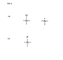
While the region directly under a gate insulating film functions as a channel region of the transistor, terminal sections of silicon constituting this channel region are, in form, either remaining unbound (the dangling bond) or bonded to a hydrogen atom, as shown in FIG. 5(a). Because the dangling bond traps the carrier and lowers the capability of the channel region to function, the dangling bonds therein are normally eliminated, in the prior art, by carrying out the hydrogen termination through a treatment of hydrogen annealing and generating the Si—H bonds. Since the bond energy of Si—H is relatively low, however, hydrogen is liable to dissociate from the bonding in course of time, resulting in generation of the dangling bond once more. As the dangling bonds increase like this, in course of time, through the use of the transistor, the degree of carrier trapping in the channel region also increases in course of time (This phenomenon is referred to as the negative bias temperature instability effect (slow trap effect), hereinafter). Once the negative bias temperature instability effect is generated, there arises a problem that the threshold voltage changes in course of time and, along with that, the drain saturation current decreases in course of time.
Such a problem resulting from generation of the negative bias temperature instability effect has not been, up to now, recognized fully or techniques to solve this problem have been hardly studied. The present invention is made to overcome problems of this sort and its immediate object is to suppress generation of the negative bias temperature instability effect and prevent the change in threshold voltage and the decrease in drain saturation current.
Further, another object of the present invention is to overcome the problem of deterioration of element characteristics that arise due to the hot electron effect. The hot electron effect is a phenomenon in which high energy electrons produced by being accelerated by the electric field between source and drain together with electrons and holes produced by the impact ionization intrude into a gate oxide film and thereby alters the MOS characteristics. In a conventional MOSFET (MOS Field Effect Transistor), silicon in a channel region has the terminal structure of Si—H with a weak bonding strength so that, in operating the transistor, channel carriers are liable to collide with and break the Si—H bonds. Such breaking of the Si—H bonds leads to the generation of an interface state, which then brings about the hot electron effect. The hot electron effect causes the threshold voltage to change and the mutual conductance gm to degrade and, thus, reduces the reliability of the element greatly. This problem is particularly pronounced in the nMOS, because a larger drain saturation current flows in the nMOS than the one in the pMOS. Further, the hot electron effect becomes more marked when the gate length becomes shortened through the element miniaturization, or a high electron field becomes applied between source and drain. It is another object of the present invention that such a problem is solved and the change in the threshold voltage as well as the degradation of the mutual conductance gm that occur due to the hot electron effect are prevented with effect.
Further, although both the suppression of the negative bias temperature instability effect and the suppression of the hot electron effect cause the same effect of preventing the change in the threshold voltage, these are essentially different issues. The change in the threshold voltage due to the negative bias temperature instability effect is brought about by gradual breaking of the Si—H bonds in a channel region and generating the dangling bonds in course of time and is an issue concerning an improvement on the long term reliability of the transistor. On the other hand, the change in the threshold voltage due to the hot electron effect is brought about through intrusion into a gate oxide film by hot electrons which are generated when the transistor is in use. In short, they are separate issues originated through different mechanisms at different places.
As described above, the present invention aims to solve the first problem that the change in the threshold voltage and the decrease in the drain saturation current due to the generation of the negative bias temperature instability effect should be prevented, and further to solve the second problem that, by suppressing the hot electron effect, the change in the threshold voltage and the degradation of the mutual conductance gm should be prevented. Especially when the present invention is applied to a pMOS, the primary object is to solve the problem of the negative bias temperature instability effect and when applied to an nMOS, the problem of the hot electron effect. The explanation lies in the fact that, in a pMOS, ON-current is considerably small so that the problem of hot electrons occur relatively infrequently and the problem of the negative bias temperature instability effect becomes more important, while in an nMOS, in contrast with that, the problem of hot electrons becomes more important. In a pMOS, negative bias is applied on a gate electrode. Therefore holes which can generate dangling bonds are introduced to the region under the gate electrode and the problem of the negative bias temperature instability effect becomes more important in a pMOS.
SUMMARY OF THE INVENTION
The present inventors conceived a novel idea to use, against the above problems, a technique in which, with fluorine being doped, the silicon terminals in a channel region is made substituted by the Si—F bonds and, recognizing its effectiveness, brought the idea to completion as the present invention, successfully.
In light of the above problems, the present invention provides a method of manufacturing a semiconductor device; which comprises the steps of:
forming a gate electrode over a gate insulating film on a silicon substrate;
introducing dopants of a given conductive-type into said gate electrode and the surface of said silicon substrate;
carrying out a first heat treatment so as to make said dopants within said silicon substrate diffuse and form a source-drain region;
doping fluorine, at least, into said gate electrode and thereafter carrying out a second heat treatment.
Further, the present invention provides a method of manufacturing a semiconductor device; which comprises the steps of:
forming a gate electrode over a gate insulating film on a silicon substrate;
introducing dopants of a given conductive-type into said gate electrode and the surface of said silicon substrate;
carrying out a first heat treatment so as to make said dopants within said silicon substrate diffuse and form a source-drain region;
forming a silicon nitride film over the entire surface;
doping fluorine, at least, into said gate electrode and thereafter carrying out a second heat treatment.
In a manufacturing method of a semiconductor device according to the present invention, after fluorine is doped, at least, into a gate electrode, a second heat treatment makes fluorine within the gate electrode diffuse and diffused fluorine bond to silicon in a region located directly under a gate insulating film. By this, the Si—H bonds and the dangling bonds shown in FIG. 5(a) are efficiently replaced with fluorine atoms to form the Si—F bonds as shown in FIG. 5(b). Since the Si—F bonds have a higher bond energy than the Si—H bonds, the phenomenon that these bonds are gradually broken in course of time and the dangling bonds are made to increase hardly ever takes place. Consequently, the negative bias temperature instability effect hardly ever generates so that the change in the threshold voltage and the decrease in drain saturation current can be prevented with effect. Further, the Si—F bonds have higher bond energy than the Si—H bonds, this method is also effective to suppress the hot electron effect. In a conventional MOSFET, breaking of the Si—H bond terminals makes an interface state generate, and, therefore, the degradation of element characteristics due to the hot electron effect is liable to happen. Against this, in the present invention, because the Si—H bonds and the dangling bonds are substituted by the Si—F bonds, such problems can be overcome with effect.
In the present invention, after a source-drain region is formed, doping of fluorine is carried out. If the order of the steps is reversed and a source-drain region is formed after doping of fluorine is carried out, not only the effects of suppressing the negative bias temperature instability effect or the like cannot be sufficiently obtained but also the problem of the more marked boron penetration may arise.
For example, in a pMOS for which BF2 + or B+ is utilized as dopants in a source-drain region, if fluorine is doped into a gate electrode before these ions are implanted thereinto, the problem of boron penetration becomes serious. On this occasion, after doping fluorine, a heat treatment is conducted for the purpose of forming the source-drain region or the like. If this heat treatment is carried out under the conditions optimum to forming the source-drain as well as eliminating the gate depletion in a gate electrode of the surface channel type, the conditions being at a high temperature in the presence of fluorine, the boron penetration is apt to become considerable. For example, in a conventional method of manufacturing a pMOS, a process in which, after BF2 + is ion-implanted over the entire surface, a source-drain region is formed by activating the dopants by a heat treatment, is widely used. In this process, the heat treatment for formation of the source-drain region is conducted in the presence of fluorine. As described above, fluorine accelerates the diffusion of boron (Japanese Patent Application Laid-open No. 330441/1996 and so forth) so that, by the above heat treatment, boron in the gate electrode is made to diffuse with a high diffusion velocity and penetrate through a gate oxide film and further diffuse into a silicon substrate.
Further, in an nMOS, if a source-drain region is formed after doping fluorine, the diffusion depth of dopants may change and the source-drain region formed may not have a prescribed depth. As the diffusion velocity of dopants is altered in the presence of fluorine, if fluorine in a gate oxide film diffuses into a silicon substrate, this fluorine may accelerate this diffusion of implanted dopants in the source-drain region and may alter the diffusion depth. Especially when doping of fluorine is applied to the entire surface of the substrate, the problem becomes considerable.
Further, when the source-drain region is formed after doping fluorine, the effects of the present invention such as suppressing the negative bias temperature instability effect cannot necessarily be obtained to the full, and, on some occasions, even element characteristics may deteriorate. When fluorine is doped in advance, a heat treatment for forming the source-drain must be carried out after doping fluorine. In this instance, if the heat treatment is conducted under the conditions favourable to form the source-drain, fluorine that is once doped in may gasify and emit from the substrate as well as the gate electrode to the outside, and, in other words, so-called out-diffusion is liable to happen. This reduces the amount of remaining fluorine within the gate electrode and the formation o the Si—F bonds may become insufficient. In recent years, rapid annealing at a high temperature such as RTA (Rapid Thermal Annealing) or the like is widely utilized as an annealing method for the formation of the source-drain, from the point of view of improving the process efficiency. The use of such a heat treatment method makes out-diffusion particularly pronounced and reduces the amount of fluorine remaining in the gate electrode.
Further, in the case that doping of fluorine is carried out in advance, there are some occasions on which the proportion of fluorine atoms that do not contribute to the generation of the Si—F bonds increases and, as a result, the effect of suppressing the negative bias temperature instability effect or the like cannot be obtained sufficiently and, furthermore, even degradation of element characteristics may be brought about. While substitution of the Si—H bonds and the dangling bonds to the Si—F bonds is made by carrying out a heat treatment after doping fluorine, the extent of the proceeding of this substitution reaction is determined by a balance between the diffusion of fluorine and the generation of the Si—F bonds. Therefore, the heat treatment for forming the Si—F bonds is preferably made under the optimum conditions, depending on the amount of doped fluorine and other conditions. Yet, when the heat treatment for forming the source-drain is performed after doping fluorine, it is the conditions for this heat treatment that determine a balance between the diffusion of fluorine and the generation of the Si—F bonds. Since the heat treatment for forming the source-drain is, in general, performed at a high temperature, the diffusion of fluorine takes precedence over the generation of the Si—F bonds and, as a result, the proportion of fluorine atoms that do not contribute to the generation of the Si—F bonds tends to increase. If this happens, the generation rate of the Si—F bonds decreases and the effects of the present invention cannot be obtained to the full, and, on some occasions, even the element characteristics may deteriorate because of the diffusion of unbound fluorine atoms that takes place in the later steps. For example, thermal diffusion of unbound fluorine atoms may take place in a silicon substrate or in an interlayer insulating film that is to be formed in a later step and result in the degradation of the transistor characteristics. There are also cases in which some of unbound fluorine atoms remain in a gate electrode and cause the boron penetration not only in the step of the heat treatment for forming the source-drain but also in the later step of another heat treatment. Accordingly, in the present invention, a second heat treatment is performed so as to prevent unbound fluorine atoms from remaining.
The above points considered, in the present invention, the fluorine doping is carried out after the formation of a source-drain region.
Meanwhile, with respect to the fluorine doping, though it is to be carried out before the formation of a source-drain region, there has been reported another example for which investigations were made for a purpose other than the one the present invention has. In Japanese Patent Application Laid-open No. 251463/1993, there is described a method of manufacturing a FET with a LDD (Lightly Doped Drain) structure wherein fluorine is doped into a gate oxide film prior to the formation of a sidewall. In forming the LDD structure, ion implantation for the formation of the LDD is first carried out, and thereafter a sidewall is formed and, then, using this sidewall as a mask, another ion implantation for the formation of a source-drain region is performed. In short, the above method is the one in which the source-drain region is formed after the fluorine doping. By performing the fluorine doping in this order, the art disclosed in the above publication sought to achieve suppressing the change in threshold voltage and the decrease in carrier mobility at the time of carrier injection. In other words, the change in the threshold voltage which is brought about by injection of hot carriers into a gate oxide film is suppressed through formation of the Si—F bonds in the gate oxide film in advance. When the fluorine doping is carried out in this order, however, the heat treatment for forming the source-drain is conducted in a state where fluorine is present within the gate oxide film so that the boron penetration tends to become considerable. Further, out-diffusion of fluorine also becomes pronounced and, moreover, because the diffusion of fluorine takes precedence over the generation of the Si—F bonds, the Si—F bonds are not necessarily formed to the full in the channel region and, therefore, there cannot be obtained sufficient effects of suppressing the negative bias temperature instability effect or the like, which is the very object of the present invention.
As described above, manufacturing processes in which the fluorine doping is performed for a purpose other than the suppression of the negative bias temperature instability effect have been investigated before, although in these processes, the fluorine doping is performed before the formation of a source-drain region. The problem of the negative bias temperature instability effect has been hardly ever recognized and, consequently, measures to overcome this problem have not been much studied. With investigations conducted by the present inventors, it was established that such a problem can be solved effectively by performing the fluorine doping and, at the same time, arranging that this fluorine doping is carried out after forming a source-drain region. The present invention is brought to completion on the basis of such an understanding.
The fluorine doping in the present invention is preferably carried out after a source-drain region is formed and then a silicon nitride film is also formed over the entire surface. With a silicon nitride film being formed, the out-diffusion of fluorine can be prevented and, thus, the Si—F bonds can be formed sufficiently. Further, as the rate of fluorine atoms remaining in a gate electrode or a substrate increases, the amount of fluorine to be doped can be reduced to the required minimum which is a clear advantage upon setting the steps of a manufacturing process. In a manufacturing process wherein a silicon nitride film is not formed, a considerable amount of fluorine must be introduced, because there are always more than a certain proportion of the doped fluorine atoms that do not contribute to the generation of the Si—F bonds. When a large amount of fluorine is doped, however, unless annealing is sufficiently carried out, there are occasions on which fluorine gas is confined within an upper layer such as an interlayer insulating film or its interface, causing a film to swell or peel off. Because of this, it is necessary to set an annealing time considerably long so as to gasify superfluous fluorine thoroughly to remove. This may result in lowering the process efficiency. Further, there are even cases in which it becomes difficult to control the remaining fluorine properly. In contrast with this, if the fluorine doping is carried out after forming a silicon nitride film, the process efficiency can be raised and besides, the degradation of element characteristics due to the fluorine diffusion that may occur in the later steps can be prevented. Further, this silicon nitride film can serve as an etching stopper film in the later steps of forming a contact hole and thereby can prevent the leakage of current, which is another advantage.
BRIEF DESCRIPTION OF THE DRAWINGS
FIGS. 1(a)-1(c) are a series of schematic cross-sectional views illustrating the steps of a method of manufacturing a semiconductor device in accordance with the present invention.
FIGS. 2(a)-2(d) are a series of schematic cross-sectional views illustrating further steps of the method of manufacturing a semiconductor device in accordance with the present invention.
FIGS. 3(a) and 3(b) are a series of schematic cross-sectional views illustrating further steps of the method of manufacturing a semiconductor device in accordance with the present invention.
FIGS. 4(a) and 4(b) are a series of schematic cross-sectional views illustrating further steps of the method of manufacturing a semiconductor device in accordance with the present invention.
FIGS. 5(a) and 5(b) are a pair of views in explaining the structure of the terminal section of silicon.
FIG. 6 is a graph in explaining the effect of the negative bias temperature instability effect improvement obtained under the application of the present invention.
FIGS. 7(a)-7(c) are a series of schematic cross-sectional views illustrating the steps of another method of manufacturing a semiconductor device in accordance with the present invention.
FIGS. 8(a)-8(c) are a series of schematic cross-sectional views illustrating further steps of the method of manufacturing a semiconductor device in accordance with the present invention.
FIGS. 9(a)-9(c) are a series of schematic cross-sectional views illustrating further steps of the method of manufacturing a semiconductor device in accordance with the present invention.
FIG. 10 is a graph in explaining the effect of the negative bias temperature instability effect improvement obtained under the application of the present invention.
DETAILED DESCRIPTION OF THE PREFERRED EMBODIMENTS
In a manufacturing method of a semiconductor device according to the present invention, a gate electrode is first formed over a gate insulating film on a silicon substrate. For the gate insulating film, for example, a silicon thermal oxide film is utilized. The gate electrode is made of polysilicon, a refractory metal or the like, or alternatively multi-layered in structure using these materials together. As for the method of forming a gate electrode, there is no specific limitation and, for example, a method in which a gate insulating film and a gate electrode layer are formed, and thereafter patterning is carried out by selective etching is employed.
Next, dopants of a given conductive-type are introduced into the gate electrode and the surface of the silicon substrate. With respect to the silicon substrate, dopants are normally introduced into the regions on both sides of the gate electrode. The doping is carried out, for example, by the ion implantation method. As described above, by introducing dopants both into the gate electrode and into the silicon substrate in one and the same step, the process efficiency can be raised.
Next, a first heat treatment is performed. While this heat treatment makes the dopants in the silicon substrate diffuse and forms a source-drain region, normally, this treatment concurrently activates the dopants in the gate electrode so as to improve a conductivity of the gate electrode. The conditions for the first heat treatment are appropriately set, depending on the doping conditions and so forth. For example, when the doping is carried out by the ion implantation method, the conditions for this heat treatment are determined, according to the implantation species, the acceleration voltage, the dose and the like. Further, if the heat treatment mentioned above is performed by the RTA, the dopants can be activated within a short time and adverse effects on the dopant distribution in the dopant diffusion layer or on the elements disposed on the substrate can be well controlled. Especially when a shallow diffusion layer is formed, the heat treatment by the RTA is effective. To use the RTA, the treatment temperature is normally set to be 900 to 1100° C.
Next, if required, after a silicon nitride film is formed, fluorine is doped, at least, into the gate electrode and, then, a second heat treatment is carried out. With regard to the fluorine doping, various methods, including the ion implantation method and the thermal diffusion method can be utilized, and, further, considering the process efficiency, the entire surface of the substrate, instead of the gate electrode alone, can be subjected to the doping. When the ion implantation method is used, the dose is preferably 1×1013 cm−2-1×1016 cm−2, and more preferably 5×1014 cm−2-3×1015 cm−2. The acceleration voltage is preferably 5-30 keV and more preferably 5-20 keV. With such conditions of the ion implantation taken, the fluorine can be doped sufficiently without giving any damage to the substrate.
In the case that the doping is made by the thermal diffusion method, a method in which a heat treatment is conducted in a gas containing fluorine such as NF3 or the like is used, for example. The temperature for the heat treatment is, for example, 700-950° C. and preferably 750 to 900° C. If the temperature for the heat treatment is set too high, the dopant distribution in the source-drain region may be affected and, in the pMOS, even the boron penetration may take place. On the other hand, if the temperature for the heat treatment is set too low, fluorine may not be sufficiently doped thereinto.
The second heat treatment after the fluorine doping is performed in order that fluorine may diffuse and migrate into a region of the gate insulating film so as to substitute the terminal sections of silicon in that region to the Si—F bonds efficiently. The treatment temperature for the second heat treatment is preferably 500 to 900° C. and more preferably 600 to 800° C. If the temperature for the heat treatment is set too high, the out-diffusion of fluorine may become pronounced or the diffusion of fluorine may take precedence over the generation of the Si—F bonds, resulting in the insufficient formation of the Si—F bonds. In addition, the boron penetration may take place and, further, the dopant concentration profile in the source-drain region may be changed. On the other hand, if the temperature for the heat treatment is set too low, fluorine may not be introduced thereinto sufficiently. When the second heat treatment is carried out in the above temperature range, the fluorine atoms introduced thereinto substitute efficiently the Si—H bonds and the dangling bonds of silicon that constitute the channel region or the like to form the Si—F bonds so that the negative bias temperature instability effect and the hot electron effect can be suppressed still more effectively. Further, the proportion of the fluorine atoms that do not contribute the bonding can be reduced and, therefore, the degradation of the element characteristics that is caused by fluorine of that sort can be well suppressed.
In the present invention, if a silicon nitride film is formed prior to the doping of fluorine, it is preferable to form the film by the LP (Low-Pressure) CVD method. Using this method, the dense nature of the film can be improved further so that the out-diffusion of fluorine can be prevented with effect. As for the conditions of the film formation, preferably, the temperature is set to be 600 to 750° C. and the growth time, 1-7 hours. Under these conditions, the dense nature of the film can be improved still further.
The present invention is particularly effective when applied to a MOSFET whose gate electrode has a width of 0.2 μm or less or a MOSFET whose gate insulating film has a thickness of 4 nm or less, since the change in the threshold voltage due to the negative bias temperature instability effect or the hot electron effect exerts a large influence upon these FETs with advanced miniaturization.
When the present invention is applied to a pMOS, especially to a pMOS of the surface channel type having a p-type electrode, the problem of the negative bias temperature instability effect can be solved very much with effect. The explanation lies in the fact that the drain saturation current in the pMOS is small in comparison with that in the nMOS, and, consequently, the effect of the negative bias temperature instability effect therein tends to become considerable. Especially in the pMOS of the surface channel type, in addition to that, the channel region is narrow so that the effect of the negative bias temperature instability effect becomes still more marked. Accordingly, the present invention can solve the problem of the negative bias temperature instability effect still more effectively in case boron is utilized as dopants and, moreover, in case it is applied to a manufacturing process wherein a source-drain region with a shallow junction is formed by the ion implantation method with an acceleration voltage of 8 keV or less.
Further, when the present invention is applied to an nMOS, the problem of the hot electron effect rather than that for suppressing the negative bias temperature instability effect can be solved with effect. This results from the fact that in the nMOS, the drain saturation current is large in comparison with that in the pMOS so that the hot electron effect becomes more significant. On this occasion, arsenic, phosphorus, antimony or the like is utilized as dopants in the source-drain region.
FIRST EXAMPLE
The present example illustrates a case in which the present invention is applied to a process of manufacturing a CMOS (Complementary MOS). Referring to FIGS. 1-4, the present Example is described below.
First, as shown in FIG. 1(a), after element isolation films 2 were formed on a silicon substrate 1 by means of STI (Shallow Trench Isolation), a resist mask 3 was formed in an nMOS formation region and, then, phosphorus was ion-implanted into a pMOS formation region, and thereby an n-type well 4 was formed. Subsequently, with the resist mask 3 being left as it was, arsenic was injected as channel dopants in order to adjust the threshold voltage. The conditions of the ion implantation were that the acceleration voltage was 100 keV and the dose was 7×1012 cm−2.
Next, as shown in FIG. 1(b), a resist mask 5 was set in the pMOS formation region and, then, boron was ion-implanted into the nMOS formation region, and thereby a p-type well 6 was formed. Subsequently, with the resist mask 5 being left as it was, boron was injected as channel dopants in order to adjust the threshold voltage. The conditions of the ion implantation were that the acceleration voltage was 30 keV and the dose was 8×1012 cm−2.
Following this, by carrying out the pyrogenic oxidation at 850° C., a gate oxide film 7 with a thickness of 4 nm was formed on the surface of the active region and thereafter a polysilicon film 8 was deposited thereon to a thickness of 150 nm. These two films were then patterned by selective etching (FIG. 1(c)). The gate length for respective gate electrodes was set to be 0.18 μm.
Next, as shown in FIG. 2(a), a resist mask 12 was set in the nMOS formation region and the ion implantation was applied to the pMOS formation region, and thereby a source-drain extension region 13 being doped to a high concentration was formed. The ion species, hereat, was BF2, the acceleration voltage was 5 keV and the dose was 1×1014 cm−2. Next, with the resist mask 12 being left as it was, ion implantation for forming a pocket region 14 was performed. This ion implantation was conducted by the rotational implantation method at an injection angle of 25°. Arsenic was utilized as the ion species and the acceleration voltage was set to be 70 keV and the dose, 2×1013 cm−2.
Next, as shown in FIG. 2(b), a resist mask 15 was set in the pMOS formation region and the ion implantation was applied to the nMOS formation region, and thereby a source-drain extension region 16 being doped to a high concentration was formed. The ion species, hereat, was arsenic, the acceleration voltage was 10 keV and the dose was 4×1014 cm−2. Next, with the resist mask 15 being left as it was, ion implantation for forming a pocket region 17 was performed. This ion implantation was conducted by the rotational implantation method at an injection angle of 25°. BF2 was utilized as the ion species and the acceleration voltage was set to be 30 keV and the dose, 4×1013 cm−2.
Next, a sidewall 18 as well as a sidewall 19 was formed by a well-known conventional method, accomplishing a gate electrode 20 as well as a gate electrode 21 (FIG. 2(c)). Subsequently, boron was ion-implanted into the pMOS formation region. Through this, the formation of a source-drain region 22 and the doping into the gate electrode 20 were simultaneously achieved (FIG. 2(d)). The conditions for the boron implantation were that the acceleration voltage was 5 keV and the dose was 4×1015 cm−2.
Subsequently, arsenic was ion-implanted into the nMOS formation region. Through this, the formation of a source-drain region 23 and the doping into the gate electrode 21 were simultaneously achieved (FIG. 2(d)). The conditions for the implantation were that the acceleration voltage was 50 keV and the dose was 6×1015 cm−2. After this, in a nitrogen atmosphere, a RTA treatment was conducted at 1050° C. for 10 seconds and the dopants within the source-drain regions and the gate electrodes were activated. FIG. 2(d) represents the state after the steps thus far have been completed.
Next, as shown in FIG. 3(a), the entire surface was subjected to the ion implantation of fluorine 24. The implantation conditions were that the acceleration voltage was 10 keV and the dose was 3×1015 cm−2. When the ion implantation was performed under these conditions, the range of fluorine stayed in the gate electrodes and the vicinity of the surface of the silicon substrate. After the doping of fluorine, as shown in FIG. 3(b), in a nitrogen atmosphere, a heat treatment was conducted at 700° C. for 20 minutes. By this, fluorine in the gate electrodes reached the channel regions 26 lying directly under the gate insulating film 7 through thermal diffusion. The terminal section of silicon constituting the channel regions 26 was, in form, as shown in FIG. 5(a), either bonded to a hydrogen atom or remaining unbound, but, in either case, it was readily replaced with a fluorine atom to take the form shown in FIG. 5(b). That is, the Si—H bonds and the dangling bonds of silicon constituting the channel regions 26 were substituted by fluorine atoms efficiently.
Subsequently, after a cobalt film was formed by the sputtering method, cobalt silicide 27 was formed by applying a heat treatment (FIG. 4(a)). Cobalt silicide 27 was formed, as shown in the drawing, on the gate electrodes and on the source-drain regions. The film thickness of cobalt silicide 27 was approximately 35 nm.
Next, after a BPSG (Boro-Phospho Silicate Glass) film 28 was formed over the entire surface as an interlayer insulating film, contact holes were set and then tungsten plugs 29 were formed by means of well-known CMP (Chemical Mechanical Polishing) (FIG. 4(b)). After that, upper layer interconnections and the like were formed by a well-known method, and thereby a CMOS was accomplished.
For a pMOS included in a CMOS that was manufactured in the above method, an evaluation of characteristics of the negative bias temperature instability effect resistance was made. In addition, other pMOSs which were manufactured in the same way as the above but with altered amounts of the fluorine doping were also evaluated. The amounts of the fluorine doping for respective samples are summarized in Table 1. The pMOS described in the above Example is Sample No. 2. Sample No. 4 is a conventional pMOS into which no fluorine was doped.
TABLE 1
Dose of Acceleration voltage
the fluorine doping at the time of fluorine
NO. (cm−3) doping (keV)
1 6 × 10¹⁵ 10
2 3 × 10¹⁵ 10
3 5 × 10¹⁴ 10
4 None
The evaluation was made by measuring changes in the threshold voltage while samples were left in an atmosphere at 200° C. When left at such a high temperature, dangling bonds are liable to be generated within the gate insulating film and the channel regions. When this happens, the generation of the negative bias temperature instability effect is accelerated and the change in the threshold voltage, increased. In other words, the evaluation method of the present Example corresponds to an accelerated test of characteristics of the negative bias temperature instability effect resistance. The evaluation results are set out in FIG. 6. It is clearly seen that Samples Nos. 1-3 manufactured by the method of the present invention show a smaller change in the threshold voltage (ΔVth) than Sample No. 4 of a conventional method, which indicates the negative bias temperature instability effect was well suppressed in Samples Nos. 1-3.
The above description shows that the present Example can improve characteristics of the negative bias temperature instability effect resistance in the pMOS of the CMOS. For the nMOS, the present Example also has the effect of suppressing the change in the threshold voltage due to hot electrons, though not shown.
SECOND EXAMPLE
A CMOS was manufactured in the same way as First Example (Sample No. 2) except that the ion implantation of fluorine was carried out after a silicon nitride film was formed and that the heat treatment after the fluorine doping was not performed. Referring to the drawings, a manufacturing process of the present example is described below.
First, the same steps as illustrated in FIGS. 1-2 of First Example were carried out.
Next, after a cobalt film was formed by the sputtering method, cobalt silicide 27 was formed by applying a heat treatment (FIG. 7(a)). The film thickness of cobalt silicide 27 was approximately 35 nm.
Next, a silicon nitride film 30 (with a film thickness of 50 nm) was formed over the entire surface by the LP-CVD method (FIG. 7(b)). The growth temperature was set to be 630° C.
Next, as shown in FIG. 7(c), the entire surface was subjected to the ion implantation of fluorine 24. The implantation conditions were that the acceleration voltage was 10 keV and the dose was 5×1014 cm−2. No heat treatment was performed after do-ping fluorine.
Next, after a BPSG film 28 was formed over the entire surface as an interlayer insulating film (FIG. 8(a)), a resist mask 31 was set thereon (FIG. 8(b)) and then contact holes 32 were formed (FIG. 8(c)). The dry etching was carried out, using an etching gas in which CO, Ar and O2 were added to C4F8. Since this etching gas has a high etching selection ratio of the silicon oxide film to the silicon nitride film, a silicon oxide film could be etched selectively. Because of this, etching of the BPSG film 28 shown in FIG. 8(c) was stopped above the silicon nitride film 30. The film thickness of the BPSG film was 100 nm or so and considerably thick so that a certain amount of over-etching was necessary in carrying out the above etching. As a result, there were, hitherto, some occasions on which the dopant diffusion layers were also etched and, due to this, a faulty formation of contact plugs was brought about. Against this, in the present invention, a silicon nitride film was set as an etching stopper film so that problems of this sort could be avoided.
After the BPSG film 28 was etched, the silicon nitride film 30 was then removed by dry etching. The etching gas used hereat was a gas containing CHF3 and O2. Since this etching gas etches the silicon nitride film 30 selectively over the cobalt silicide 27, the above-mentioned dry etching was stopped above the cobalt silicide 27 (FIG. 9(a)). Without this cobalt silicide 27, the source-drain regions may be etched, which may cause the leakage of the current.
After the etching was completed, the resist mask 31 was removed and, then, a Ti film 34 (with a film thickness of 10 nm) and a TiN film 35 (with a film thickness of 50 nm) were formed, in this order. After that, in a nitrogen atmosphere, an annealing treatment was conducted by the RTA method at 690° C. for 30 seconds. At this, doped fluorine diffused within the gate electrode and reached the channel regions 26 lying directly under the gate insulating films 7. Accordingly, the Si—H bonds and the dangling bonds of silicon constituting the channel regions 26 were substituted by fluorine atoms efficiently.
Subsequently, after tungsten 36 was deposited over the entire surface by the sputtering method, tungsten plugs were formed by means of well-known CMP. After that, upper layer interconnections and the like were formed by a well-known method, and thereby a CMOS was accomplished.
For a pMOS included in a CMOS manufactured in the above method, an evaluation of characteristics of the negative bias temperature instability effect resistance was made. The evaluated FETs are summarized in Table 2. Sample No. 1 is a pMOS manufactured in the above method. In addition, other pMOSs into which no fluorine was doped were also evaluated (Samples Nos. 2, 3). Sample No. 2 is a conventional CMOS obtained by a method in which no silicon nitride film was formed and similar to Sample No. 4 in Table 1. Sample No. 3 is a CMOS obtained by a method in which a silicon nitride film was formed and manufactured in the same way as Sample No. 1 except that the step of doping fluorine shown in FIG. 7(c) was not performed.
TABLE 2
Dose of Acceleration voltage
the fluorine at the time of
doping fluorine
NO. (cm−2) doping (keV) SiN deposition
1 5 × 10¹⁴ 10 Yes
2 None No
3 None Yes
The evaluation was made by measuring changes in the threshold voltage while samples were left in an atmosphere at 200° C. When left at such a high temperature, dangling bonds are liable to be generated within the gate insulating film and the channel regions. When this happens, the generation of the negative bias temperature instability effect is accelerated and the change in the threshold voltage, increased. In other words, the evaluation method of the present Example corresponds to an accelerated test of characteristics of the negative bias temperature instability effect resistance. The evaluation results are set out in FIG. 10. It is clearly seen that Sample No. 1 manufactured by the method of the present invention show a smaller change in the threshold voltage than Samples Nos. 2-3, which indicates the negative bias temperature instability effect was well suppressed in Sample No. 1. Furthermore, in comparison with the manufacturing process of First Example, this process of the present Example can reduce the amount of the fluorine doping and besides, it has an advantage that the heat treatment after the fluorine doping can be also used as a heat treatment of another step thereof (In the present Example, it was used as a heat treatment of the annealing step after the Ti/TiN films were formed).
The above description shows that the present Example can improve characteristics of the negative bias temperature instability effect resistance in the pMOS of the CMOS. For the nMOS, the present Example also has the effect of suppressing the change in the threshold voltage due to hot electrons, though not shown.
Further, in the above Examples, the present invention is described, using a process of forming a CMOS, but it is to be understood that the present invention can be applied to the transistor formation in other devices such as a DRAM (Dynamic Random Access Memory).
As described above, in the present invention, after the formation of a source-drain region, the ion implantation with fluorine is carried out and, then, a heat treatment is conducted so that the terminal sections of silicon in the channel regions are efficiently substituted by fluorine atoms. This can suppress the negative bias temperature instability effect and improve the long-term reliability of the transistor. Further, this can effectively prevent the change in the threshold voltage and the degradation of the mutual conductance gm due to the hot electron effect.
This application is based on Japanese patent application NO.HEI11-070723, the content of which is incorporated hereinto by reference.

Claims (12)

What is claimed is:
1. A method of manufacturing a semiconductor device which comprises:
forming a gate electrode over a gate insulating film on a silicon substrate;
introducing dopants of a predetermined conductive-type into said gate electrode and a surface of said silicon substrate;
after said introducing dopants, carrying out a first heat treatment so as to make said dopants within said substrate diffuse and form a source-drain region; and
after forming said source-drain region, doping fluorine, at least into said gate electrode and thereafter carrying out a second heat treatment so as to make fluorine diffuse into a channel region of said silicon substrate.
2. The method of manufacturing a semiconductor device according to claim 1, wherein said dopants comprise boron.
3. The method of manufacturing a semiconductor device according to claim 1, wherein said dopants comprise arsenic, phosphorus or antimony.
4. The method of manufacturing a semiconductor device according to claim 1, wherein said doping of fluorine into said gate electrode is carried out by ion implantation at a dose of 1×1013 cm−2 to 1×1016 cm−2.
5. The method of manufacturing a semiconductor device according to claim 1, wherein said second heat treatment is carried out at a treatment temperature of 500 to 900° C.
6. A method of manufacturing a semiconductor device which comprises:
forming a gate electrode over a gate insulating film on a silicon substrate;
introducing dopants of a given conductive-type into said gate electrode and a surface of said silicon substrate;
carrying out a first heat treatment so as to make said dopants within said silicon substrate diffuse and form a source-drain region;
after forming said source-drain region, forming a silicon nitride film over an entire surface of said semiconductor device;
after forming said silicon nitride film, doping fluorine, at least, into said gate electrode and thereafter carrying out a second heat treatment so as to make said fluorine diffuse into a channel region of said silicon substrate.
7. The method of manufacturing a semiconductor device according to claim 6, wherein said dopants comprise boron.
8. The method of manufacturing a semiconductor device according to claim 6, wherein said dopants comprise arsenic, phosphorus or antimony.
9. The method of manufacturing of a semiconductor device according to claim 6, wherein said doping of fluorine into said gate electrode is carried out by ion implantation at a dose of 1×1013 cm−2 to 1×1016 cm−2.
10. The method of manufacturing a semiconductor device according to claim 6, wherein said second heat treatment was carried out at a treatment temperature of 500 to 900° C.
11. The method of manufacturing a semiconductor device according to claim 1, wherein a threshold voltage and drain saturation current are substantially constant over time.
12. The method of manufacturing a semiconductor device according to claim 6, wherein a threshold voltage and drain saturation current are substantially constant over time.
US09/525,904 1999-03-16 2000-03-15 Manufacturing method of semiconductor device Expired - Fee Related US6261889B1 (en)

Applications Claiming Priority (2)

Application Number Priority Date Filing Date Title
JP11070723A JP2000269492A (en) 1999-03-16 1999-03-16 Manufacture of semiconductor device
JP11-070723 1999-03-16

Publications (1)

Publication Number Publication Date
US6261889B1 true US6261889B1 (en) 2001-07-17

Family

ID=13439768

Family Applications (1)

Application Number Title Priority Date Filing Date
US09/525,904 Expired - Fee Related US6261889B1 (en) 1999-03-16 2000-03-15 Manufacturing method of semiconductor device

Country Status (4)

Country Link
US (1) US6261889B1 (en)
JP (1) JP2000269492A (en)
KR (1) KR20000076854A (en)
TW (1) TW445650B (en)

Cited By (22)

* Cited by examiner, † Cited by third party
Publication number Priority date Publication date Assignee Title
US6380021B1 (en) * 2000-06-20 2002-04-30 Taiwan Semiconductor Manufacturing Company Ultra-shallow junction formation by novel process sequence for PMOSFET
US6436783B1 (en) * 1999-09-17 2002-08-20 Nec Corporation Method of forming MOS transistor
US6528401B2 (en) * 1999-12-31 2003-03-04 Hyundai Electronics Industries Co., Ltd. Method for fabricating polycide dual gate in semiconductor device
US6657454B2 (en) 2002-03-15 2003-12-02 Solid State Measurements, Inc. High speed threshold voltage and average surface doping measurements
US6709932B1 (en) 2002-08-30 2004-03-23 Texas Instruments Incorporated Method for improving gate oxide integrity and interface quality in a multi-gate oxidation process
US20040073412A1 (en) * 2002-10-04 2004-04-15 Walker John De Quincey Negative bias temperature instability effect modeling
US6780730B2 (en) 2002-01-31 2004-08-24 Infineon Technologies Ag Reduction of negative bias temperature instability in narrow width PMOS using F2 implantation
EP1455386A2 (en) * 2003-03-04 2004-09-08 Matsushita Electric Industrial Co., Ltd. Semiconductor device and fabrication method therefor
US20050167764A1 (en) * 2004-02-03 2005-08-04 Hong-Jyh Li Transistor with doped gate dielectric
WO2005076331A1 (en) * 2004-02-02 2005-08-18 Koninklijke Philips Electronics N.V. Method of fabricating metal-oxide semiconductor integrated circuit devices.
US20050205858A1 (en) * 2004-03-22 2005-09-22 Hong-Jyh Li Transistor with shallow germanium implantation region in channel
US20050250319A1 (en) * 2004-05-04 2005-11-10 International Business Machines Corporation Stabilization of Ni monosilicide thin films in CMOS devices using implantation of ions before silicidation
US20060017132A1 (en) * 2004-06-29 2006-01-26 Infineon Technologies Ag Method for producing a dielectric and semiconductor structure
US20060097318A1 (en) * 2003-12-30 2006-05-11 Hong-Jyh Li Transistor with silicon and carbon layer in the channel region
US20060217280A1 (en) * 2002-05-17 2006-09-28 Scheper William M Automatic dishwashing compositions and methods for use with electrochemical cells and/or electrolytic devices
US20070173041A1 (en) * 2004-03-15 2007-07-26 Koninklijke Philips Electronics, N.V. Method of manufacturing a semiconductor device and semiconductor device obtained with such a method
US20070173023A1 (en) * 2006-01-24 2007-07-26 Gen Okazaki Semiconductor device manufacturing method
US20080200017A1 (en) * 2007-02-16 2008-08-21 Oki Electric Industry Co., Ltd Method of producing semiconductor device
US20100025754A1 (en) * 2008-08-01 2010-02-04 Renesas Technology Corp. Semiconductor device and a method of manufacturing the same
US20120309145A1 (en) * 2011-05-31 2012-12-06 Samsung Electronics Co., Ltd. Methods of manufacturing semiconductor devices
CN102891084A (en) * 2011-07-19 2013-01-23 中芯国际集成电路制造(上海)有限公司 Method for manufacturing P-channel metal oxide semiconductor (PMOS) transistor
US10438951B2 (en) 2017-03-24 2019-10-08 Asahi Kasei Microdevices Corporation Semiconductor device and manufacturing method thereof

Families Citing this family (9)

* Cited by examiner, † Cited by third party
Publication number Priority date Publication date Assignee Title
JP3687776B2 (en) * 1999-12-14 2005-08-24 旭化成マイクロシステム株式会社 Manufacturing method of semiconductor device
KR100368310B1 (en) * 2000-12-29 2003-01-24 주식회사 하이닉스반도체 Method of manufacturing semiconductor device
JP2004289125A (en) * 2003-03-04 2004-10-14 Matsushita Electric Ind Co Ltd Semiconductor device and manufacturing method therefor
KR100674943B1 (en) * 2005-01-15 2007-01-26 삼성전자주식회사 Sb, Ga or Bi doped Semiconductor Device and Manufacturing Method for the Same
JP5153164B2 (en) * 2007-03-07 2013-02-27 ルネサスエレクトロニクス株式会社 Manufacturing method of semiconductor device
JP2008262956A (en) 2007-04-10 2008-10-30 Elpida Memory Inc Semiconductor device and its manufacturing method
JP2008263006A (en) * 2007-04-11 2008-10-30 Elpida Memory Inc Semiconductor device and its manufacturing method
JP6234173B2 (en) * 2013-11-07 2017-11-22 ルネサスエレクトロニクス株式会社 Manufacturing method of solid-state imaging device
US9502307B1 (en) 2015-11-20 2016-11-22 International Business Machines Corporation Forming a semiconductor structure for reduced negative bias temperature instability

Citations (6)

* Cited by examiner, † Cited by third party
Publication number Priority date Publication date Assignee Title
JPH05251463A (en) 1992-03-06 1993-09-28 Nec Corp Manufacture of semiconductor device
US5571734A (en) * 1994-10-03 1996-11-05 Motorola, Inc. Method for forming a fluorinated nitrogen containing dielectric
JPH08330441A (en) 1995-05-31 1996-12-13 Sony Corp Manufacture of mos transistor
US5712208A (en) * 1994-06-09 1998-01-27 Motorola, Inc. Methods of formation of semiconductor composite gate dielectric having multiple incorporated atomic dopants
EP0908947A2 (en) * 1997-09-29 1999-04-14 Matsushita Electronics Corporation Method for fabricating semiconductor device with pMIS transistor
US6017784A (en) * 1996-06-09 2000-01-25 Fujitsu Limited Manufacture method of semiconductor device with suppressed impurity diffusion from gate electrode

Patent Citations (6)

* Cited by examiner, † Cited by third party
Publication number Priority date Publication date Assignee Title
JPH05251463A (en) 1992-03-06 1993-09-28 Nec Corp Manufacture of semiconductor device
US5712208A (en) * 1994-06-09 1998-01-27 Motorola, Inc. Methods of formation of semiconductor composite gate dielectric having multiple incorporated atomic dopants
US5571734A (en) * 1994-10-03 1996-11-05 Motorola, Inc. Method for forming a fluorinated nitrogen containing dielectric
JPH08330441A (en) 1995-05-31 1996-12-13 Sony Corp Manufacture of mos transistor
US6017784A (en) * 1996-06-09 2000-01-25 Fujitsu Limited Manufacture method of semiconductor device with suppressed impurity diffusion from gate electrode
EP0908947A2 (en) * 1997-09-29 1999-04-14 Matsushita Electronics Corporation Method for fabricating semiconductor device with pMIS transistor

Cited By (43)

* Cited by examiner, † Cited by third party
Publication number Priority date Publication date Assignee Title
US6436783B1 (en) * 1999-09-17 2002-08-20 Nec Corporation Method of forming MOS transistor
US6528401B2 (en) * 1999-12-31 2003-03-04 Hyundai Electronics Industries Co., Ltd. Method for fabricating polycide dual gate in semiconductor device
US6380021B1 (en) * 2000-06-20 2002-04-30 Taiwan Semiconductor Manufacturing Company Ultra-shallow junction formation by novel process sequence for PMOSFET
US6780730B2 (en) 2002-01-31 2004-08-24 Infineon Technologies Ag Reduction of negative bias temperature instability in narrow width PMOS using F2 implantation
US6657454B2 (en) 2002-03-15 2003-12-02 Solid State Measurements, Inc. High speed threshold voltage and average surface doping measurements
US20060217280A1 (en) * 2002-05-17 2006-09-28 Scheper William M Automatic dishwashing compositions and methods for use with electrochemical cells and/or electrolytic devices
US6709932B1 (en) 2002-08-30 2004-03-23 Texas Instruments Incorporated Method for improving gate oxide integrity and interface quality in a multi-gate oxidation process
US20040073412A1 (en) * 2002-10-04 2004-04-15 Walker John De Quincey Negative bias temperature instability effect modeling
US7138322B2 (en) 2003-03-04 2006-11-21 Matsushita Electric Industrial Co., Ltd. Semiconductor device and fabrication method therefor
EP1455386A2 (en) * 2003-03-04 2004-09-08 Matsushita Electric Industrial Co., Ltd. Semiconductor device and fabrication method therefor
US20040173843A1 (en) * 2003-03-04 2004-09-09 Matsushita Electric Industrial Co., Ltd. Semiconductor device and fabrication method therefor
EP1455386A3 (en) * 2003-03-04 2006-03-01 Matsushita Electric Industrial Co., Ltd. Semiconductor device and fabrication method therefor
US7235822B2 (en) 2003-12-30 2007-06-26 Infineon Technologies Ag Transistor with silicon and carbon layer in the channel region
US20060097318A1 (en) * 2003-12-30 2006-05-11 Hong-Jyh Li Transistor with silicon and carbon layer in the channel region
WO2005076331A1 (en) * 2004-02-02 2005-08-18 Koninklijke Philips Electronics N.V. Method of fabricating metal-oxide semiconductor integrated circuit devices.
US7368356B2 (en) 2004-02-03 2008-05-06 Infineon Technologies Ag Transistor with doped gate dielectric
US7002224B2 (en) 2004-02-03 2006-02-21 Infineon Technologies Ag Transistor with doped gate dielectric
WO2005076330A1 (en) * 2004-02-03 2005-08-18 Infineon Technologies Ag Transistor with doped gate dielectric
US20060073643A1 (en) * 2004-02-03 2006-04-06 Hong-Jyh Li Transistor with doped gate dielectric
US20050167764A1 (en) * 2004-02-03 2005-08-04 Hong-Jyh Li Transistor with doped gate dielectric
US20070173041A1 (en) * 2004-03-15 2007-07-26 Koninklijke Philips Electronics, N.V. Method of manufacturing a semiconductor device and semiconductor device obtained with such a method
US7491616B2 (en) * 2004-03-15 2009-02-17 Nxp B.V. Method of manufacturing a semiconductor device including dopant introduction
US7094671B2 (en) 2004-03-22 2006-08-22 Infineon Technologies Ag Transistor with shallow germanium implantation region in channel
US7417248B2 (en) 2004-03-22 2008-08-26 Infineon Technologies Ag Transistor with shallow germanium implantation region in channel
US20060252238A1 (en) * 2004-03-22 2006-11-09 Hong-Jyh Li Transistor with shallow germanium implantation region in channel
US20060228875A1 (en) * 2004-03-22 2006-10-12 Hong-Jyh Li Transistor with shallow germanium implantation region in channel
US20050205858A1 (en) * 2004-03-22 2005-09-22 Hong-Jyh Li Transistor with shallow germanium implantation region in channel
US7312137B2 (en) 2004-03-22 2007-12-25 Infineon Technologies Ag Transistor with shallow germanium implantation region in channel
US7119012B2 (en) * 2004-05-04 2006-10-10 International Business Machines Corporation Stabilization of Ni monosilicide thin films in CMOS devices using implantation of ions before silicidation
US20070042586A1 (en) * 2004-05-04 2007-02-22 International Business Machines Corporation STABILIZATION OF Ni MONOSILICIDE THIN FILMS IN CMOS DEVICES USING IMPLANTATION OF IONS BEFORE SILICIDATION
US7517795B2 (en) 2004-05-04 2009-04-14 International Business Machines Corporation Stabilization of Ni monosilicide thin films in CMOS devices using implantation of ions before silicidation
US20050250319A1 (en) * 2004-05-04 2005-11-10 International Business Machines Corporation Stabilization of Ni monosilicide thin films in CMOS devices using implantation of ions before silicidation
US20060017132A1 (en) * 2004-06-29 2006-01-26 Infineon Technologies Ag Method for producing a dielectric and semiconductor structure
DE102004031453B4 (en) * 2004-06-29 2009-01-29 Qimonda Ag Method for producing a dielectric and semiconductor structure
DE102004031453A1 (en) * 2004-06-29 2006-02-09 Infineon Technologies Ag Method for producing a dielectric and semiconductor structure
US20070173023A1 (en) * 2006-01-24 2007-07-26 Gen Okazaki Semiconductor device manufacturing method
US20080200017A1 (en) * 2007-02-16 2008-08-21 Oki Electric Industry Co., Ltd Method of producing semiconductor device
US20100025754A1 (en) * 2008-08-01 2010-02-04 Renesas Technology Corp. Semiconductor device and a method of manufacturing the same
US7994012B2 (en) * 2008-08-01 2011-08-09 Renesas Electronics Corporation Semiconductor device and a method of manufacturing the same
US20120309145A1 (en) * 2011-05-31 2012-12-06 Samsung Electronics Co., Ltd. Methods of manufacturing semiconductor devices
US8877579B2 (en) * 2011-05-31 2014-11-04 Samsung Electronics Co., Ltd. Methods of manufacturing semiconductor devices
CN102891084A (en) * 2011-07-19 2013-01-23 中芯国际集成电路制造(上海)有限公司 Method for manufacturing P-channel metal oxide semiconductor (PMOS) transistor
US10438951B2 (en) 2017-03-24 2019-10-08 Asahi Kasei Microdevices Corporation Semiconductor device and manufacturing method thereof

Also Published As

Publication number Publication date
TW445650B (en) 2001-07-11
JP2000269492A (en) 2000-09-29
KR20000076854A (en) 2000-12-26

Similar Documents

Publication Publication Date Title
US6261889B1 (en) Manufacturing method of semiconductor device
US5552332A (en) Process for fabricating a MOSFET device having reduced reverse short channel effects
US6383879B1 (en) Semiconductor device having a metal gate with a work function compatible with a semiconductor device
US5648287A (en) Method of salicidation for deep quarter micron LDD MOSFET devices
US6436783B1 (en) Method of forming MOS transistor
KR100226758B1 (en) Method of manufacturing cmosfet
US6465315B1 (en) MOS transistor with local channel compensation implant
US6215163B1 (en) Semiconductor device and method of manufacturing the same where the nitrogen concentration in an oxynitride insulating layer is varied
US7358128B2 (en) Method for manufacturing a transistor
US6261912B1 (en) Method of fabricating a transistor
KR100285995B1 (en) Manufacturing method of MIS transistor
US6124187A (en) Method of fabricating semiconductor device
KR20020025460A (en) Semiconductor device and fabricating method thereof
Lin et al. Suppression of boron penetration in BF/sub 2/-implanted p-type gate MOSFET by trapping of fluorines in amorphous gate
US4506279A (en) Metal-oxide-semiconductor device with bilayered source and drain
US6245624B1 (en) Methods of fabricating field effect transistors by first forming heavily doped source/drain regions and then forming lightly doped source/drain regions
US7019363B1 (en) MOS transistor with asymmetrical source/drain extensions
JP4615755B2 (en) Manufacturing method of semiconductor device
US6144094A (en) Semiconductor device including an insulation film and electrode having nitrogen added thereto
US6103582A (en) Method to suppress boron penetration in P+ mosfets
KR100463044B1 (en) Method of manufacturing semiconductor device
US6864141B1 (en) Method of incorporating nitrogen into metal silicate based dielectrics by energized nitrogen ion beams
KR100313510B1 (en) Fabrication method of semiconductor device
US7081419B2 (en) Gate dielectric structure for reducing boron penetration and current leakage
KR100334965B1 (en) Formation method of device of mos field effect transistor

Legal Events

Date Code Title Description
AS Assignment

Owner name: NEC CORPORATION, JAPAN

Free format text: ASSIGNMENT OF ASSIGNORS INTEREST;ASSIGNOR:ONO, ATSUKI;REEL/FRAME:010627/0052

Effective date: 20000303

FEPP Fee payment procedure

Free format text: PAYOR NUMBER ASSIGNED (ORIGINAL EVENT CODE: ASPN); ENTITY STATUS OF PATENT OWNER: LARGE ENTITY

AS Assignment

Owner name: NEC ELECTRONICS CORPORATION, JAPAN

Free format text: ASSIGNMENT OF ASSIGNORS INTEREST;ASSIGNOR:NEC CORPORATION;REEL/FRAME:013774/0295

Effective date: 20021101

REMI Maintenance fee reminder mailed
LAPS Lapse for failure to pay maintenance fees
STCH Information on status: patent discontinuation

Free format text: PATENT EXPIRED DUE TO NONPAYMENT OF MAINTENANCE FEES UNDER 37 CFR 1.362

FP Lapsed due to failure to pay maintenance fee

Effective date: 20050717