US6251560B1 - Photoresist compositions with cyclic olefin polymers having lactone moiety - Google Patents
Photoresist compositions with cyclic olefin polymers having lactone moiety Download PDFInfo
- Publication number
- US6251560B1 US6251560B1 US09/566,395 US56639500A US6251560B1 US 6251560 B1 US6251560 B1 US 6251560B1 US 56639500 A US56639500 A US 56639500A US 6251560 B1 US6251560 B1 US 6251560B1
- Authority
- US
- United States
- Prior art keywords
- cyclic olefin
- photoresist
- moiety
- composition
- substrate
- Prior art date
- Legal status (The legal status is an assumption and is not a legal conclusion. Google has not performed a legal analysis and makes no representation as to the accuracy of the status listed.)
- Expired - Lifetime
Links
- 0 *.*CC1CC2CC1C1C3CC(C(C)C3C)C21.CC1C(C)C2CC1C1C3*CC(C3)C21.CC1CC(C)C2C3CC(C(C)C3C)C12 Chemical compound *.*CC1CC2CC1C1C3CC(C(C)C3C)C21.CC1C(C)C2CC1C1C3*CC(C3)C21.CC1CC(C)C2C3CC(C(C)C3C)C12 0.000 description 1
- HXSXHIHLNWZNQH-UHFFFAOYSA-N C.CC.CC1C(C)C2CC1C1C3CCC(C3)C21 Chemical compound C.CC.CC1C(C)C2CC1C1C3CCC(C3)C21 HXSXHIHLNWZNQH-UHFFFAOYSA-N 0.000 description 1
- DVHHWFYLRKHCQV-UHFFFAOYSA-N C.CC.CC1C(C)C2CC1C1C3CCC(C3)C21.[V] Chemical compound C.CC.CC1C(C)C2CC1C1C3CCC(C3)C21.[V] DVHHWFYLRKHCQV-UHFFFAOYSA-N 0.000 description 1
- NUOXUMBCDKTGQR-UHFFFAOYSA-M C.CC1C(C)C2CC1C1CCCOC(=O)C21.CC1C(C)C2CC1C1CCOC(=O)C21.CC1C(C)C2CC1C1COC(=O)C21.CC1C2CC(C1C)C1(CCC(=O)OC1)C2.CC1C2CC(C1C)C1(CCCC(=O)OC1)C2.CC1C2CC(C1C)C1(COC(=O)C1)C2.CC1C2CC(C3CCC(=O)OC3)C(C2)C1C.CC1C2CC(C3CCCC(=O)OC3)C(C2)C1C.CC1C2CC(C3COC(=O)C3)C(C2)C1C.CC1C2CC(CC3COC(=O)C3)C(C2)C1C.[V]I Chemical compound C.CC1C(C)C2CC1C1CCCOC(=O)C21.CC1C(C)C2CC1C1CCOC(=O)C21.CC1C(C)C2CC1C1COC(=O)C21.CC1C2CC(C1C)C1(CCC(=O)OC1)C2.CC1C2CC(C1C)C1(CCCC(=O)OC1)C2.CC1C2CC(C1C)C1(COC(=O)C1)C2.CC1C2CC(C3CCC(=O)OC3)C(C2)C1C.CC1C2CC(C3CCCC(=O)OC3)C(C2)C1C.CC1C2CC(C3COC(=O)C3)C(C2)C1C.CC1C2CC(CC3COC(=O)C3)C(C2)C1C.[V]I NUOXUMBCDKTGQR-UHFFFAOYSA-M 0.000 description 1
- QTANAPDJDKQQQC-UHFFFAOYSA-N CC.CC.CC1C(C)C2CC1C1C3CCC(C3)C21.CC1C2CCC(C2)C1C.II Chemical compound CC.CC.CC1C(C)C2CC1C1C3CCC(C3)C21.CC1C2CCC(C2)C1C.II QTANAPDJDKQQQC-UHFFFAOYSA-N 0.000 description 1
- LGNJRJHUFXINAJ-UHFFFAOYSA-M CC.CC.CC1C(C)C2CC1C1C3CCC(C3)C21.CC1C2CCC(C2)C1C.[V]I Chemical compound CC.CC.CC1C(C)C2CC1C1C3CCC(C3)C21.CC1C2CCC(C2)C1C.[V]I LGNJRJHUFXINAJ-UHFFFAOYSA-M 0.000 description 1
Classifications
-
- G—PHYSICS
- G03—PHOTOGRAPHY; CINEMATOGRAPHY; ANALOGOUS TECHNIQUES USING WAVES OTHER THAN OPTICAL WAVES; ELECTROGRAPHY; HOLOGRAPHY
- G03F—PHOTOMECHANICAL PRODUCTION OF TEXTURED OR PATTERNED SURFACES, e.g. FOR PRINTING, FOR PROCESSING OF SEMICONDUCTOR DEVICES; MATERIALS THEREFOR; ORIGINALS THEREFOR; APPARATUS SPECIALLY ADAPTED THEREFOR
- G03F7/00—Photomechanical, e.g. photolithographic, production of textured or patterned surfaces, e.g. printing surfaces; Materials therefor, e.g. comprising photoresists; Apparatus specially adapted therefor
- G03F7/004—Photosensitive materials
- G03F7/0045—Photosensitive materials with organic non-macromolecular light-sensitive compounds not otherwise provided for, e.g. dissolution inhibitors
-
- C—CHEMISTRY; METALLURGY
- C07—ORGANIC CHEMISTRY
- C07C—ACYCLIC OR CARBOCYCLIC COMPOUNDS
- C07C41/00—Preparation of ethers; Preparation of compounds having groups, groups or groups
- C07C41/01—Preparation of ethers
- C07C41/05—Preparation of ethers by addition of compounds to unsaturated compounds
- C07C41/06—Preparation of ethers by addition of compounds to unsaturated compounds by addition of organic compounds only
-
- C—CHEMISTRY; METALLURGY
- C07—ORGANIC CHEMISTRY
- C07C—ACYCLIC OR CARBOCYCLIC COMPOUNDS
- C07C5/00—Preparation of hydrocarbons from hydrocarbons containing the same number of carbon atoms
- C07C5/02—Preparation of hydrocarbons from hydrocarbons containing the same number of carbon atoms by hydrogenation
- C07C5/08—Preparation of hydrocarbons from hydrocarbons containing the same number of carbon atoms by hydrogenation of carbon-to-carbon triple bonds
- C07C5/09—Preparation of hydrocarbons from hydrocarbons containing the same number of carbon atoms by hydrogenation of carbon-to-carbon triple bonds to carbon-to-carbon double bonds
-
- C—CHEMISTRY; METALLURGY
- C08—ORGANIC MACROMOLECULAR COMPOUNDS; THEIR PREPARATION OR CHEMICAL WORKING-UP; COMPOSITIONS BASED THEREON
- C08F—MACROMOLECULAR COMPOUNDS OBTAINED BY REACTIONS ONLY INVOLVING CARBON-TO-CARBON UNSATURATED BONDS
- C08F2/00—Processes of polymerisation
- C08F2/38—Polymerisation using regulators, e.g. chain terminating agents, e.g. telomerisation
-
- C—CHEMISTRY; METALLURGY
- C08—ORGANIC MACROMOLECULAR COMPOUNDS; THEIR PREPARATION OR CHEMICAL WORKING-UP; COMPOSITIONS BASED THEREON
- C08F—MACROMOLECULAR COMPOUNDS OBTAINED BY REACTIONS ONLY INVOLVING CARBON-TO-CARBON UNSATURATED BONDS
- C08F232/00—Copolymers of cyclic compounds containing no unsaturated aliphatic radicals in a side chain, and having one or more carbon-to-carbon double bonds in a carbocyclic ring system
-
- C—CHEMISTRY; METALLURGY
- C08—ORGANIC MACROMOLECULAR COMPOUNDS; THEIR PREPARATION OR CHEMICAL WORKING-UP; COMPOSITIONS BASED THEREON
- C08G—MACROMOLECULAR COMPOUNDS OBTAINED OTHERWISE THAN BY REACTIONS ONLY INVOLVING UNSATURATED CARBON-TO-CARBON BONDS
- C08G61/00—Macromolecular compounds obtained by reactions forming a carbon-to-carbon link in the main chain of the macromolecule
- C08G61/02—Macromolecular compounds containing only carbon atoms in the main chain of the macromolecule, e.g. polyxylylenes
- C08G61/04—Macromolecular compounds containing only carbon atoms in the main chain of the macromolecule, e.g. polyxylylenes only aliphatic carbon atoms
- C08G61/06—Macromolecular compounds containing only carbon atoms in the main chain of the macromolecule, e.g. polyxylylenes only aliphatic carbon atoms prepared by ring-opening of carbocyclic compounds
- C08G61/08—Macromolecular compounds containing only carbon atoms in the main chain of the macromolecule, e.g. polyxylylenes only aliphatic carbon atoms prepared by ring-opening of carbocyclic compounds of carbocyclic compounds containing one or more carbon-to-carbon double bonds in the ring
-
- C—CHEMISTRY; METALLURGY
- C09—DYES; PAINTS; POLISHES; NATURAL RESINS; ADHESIVES; COMPOSITIONS NOT OTHERWISE PROVIDED FOR; APPLICATIONS OF MATERIALS NOT OTHERWISE PROVIDED FOR
- C09J—ADHESIVES; NON-MECHANICAL ASPECTS OF ADHESIVE PROCESSES IN GENERAL; ADHESIVE PROCESSES NOT PROVIDED FOR ELSEWHERE; USE OF MATERIALS AS ADHESIVES
- C09J123/00—Adhesives based on homopolymers or copolymers of unsaturated aliphatic hydrocarbons having only one carbon-to-carbon double bond; Adhesives based on derivatives of such polymers
- C09J123/02—Adhesives based on homopolymers or copolymers of unsaturated aliphatic hydrocarbons having only one carbon-to-carbon double bond; Adhesives based on derivatives of such polymers not modified by chemical after-treatment
- C09J123/04—Homopolymers or copolymers of ethene
- C09J123/06—Polyethene
-
- G—PHYSICS
- G03—PHOTOGRAPHY; CINEMATOGRAPHY; ANALOGOUS TECHNIQUES USING WAVES OTHER THAN OPTICAL WAVES; ELECTROGRAPHY; HOLOGRAPHY
- G03F—PHOTOMECHANICAL PRODUCTION OF TEXTURED OR PATTERNED SURFACES, e.g. FOR PRINTING, FOR PROCESSING OF SEMICONDUCTOR DEVICES; MATERIALS THEREFOR; ORIGINALS THEREFOR; APPARATUS SPECIALLY ADAPTED THEREFOR
- G03F7/00—Photomechanical, e.g. photolithographic, production of textured or patterned surfaces, e.g. printing surfaces; Materials therefor, e.g. comprising photoresists; Apparatus specially adapted therefor
- G03F7/004—Photosensitive materials
- G03F7/039—Macromolecular compounds which are photodegradable, e.g. positive electron resists
- G03F7/0392—Macromolecular compounds which are photodegradable, e.g. positive electron resists the macromolecular compound being present in a chemically amplified positive photoresist composition
- G03F7/0395—Macromolecular compounds which are photodegradable, e.g. positive electron resists the macromolecular compound being present in a chemically amplified positive photoresist composition the macromolecular compound having a backbone with alicyclic moieties
Definitions
- microelectronics industry as well as in other industries involving construction of microscopic structures (e.g. micromachines, magnetoresistive heads, etc.), there is a continued desire to reduce the size of structural features.
- the desire is to reduce the size of microelectronic devices and/or to provide greater amount of circuitry for a given chip size.
- the ability to produce smaller devices is limited by the ability of photolithographic techniques to reliably resolve smaller features and spacings.
- the nature of optics is such that the ability to obtain finer resolution is limited in part by the wavelength of light (or other radiation) used to create the lithographic pattern.
- the trend has been to move from so-called I-line radiation (350 nm) to 248 nm radiation.
- a photoresist composition While a photoresist composition must possess desirable optical characteristics to enable image resolution at a desired radiation wavelength, the photoresist composition must also possess suitable chemical and mechanical properties to enable transfer to the image from the patterned photoresist to an underlying substrate layer(s). Thus, a patternwise exposed positive photoresist must be capable of appropriate dissolution response (i.e. selective dissolution of exposed areas) to yield the desired photoresist structure. Given the extensive experience in the photolithographic arts with the use of aqueous alkaline developers, it is important to achieve appropriate dissolution behavior in such commonly used developer solutions.
- the patterned photoresist structure (after development) must be sufficiently resistant to enable transfer of the pattern to the underlying layer(s).
- pattern transfer is performed by some form of wet chemical etching or ion etching.
- the ability of the patterned photoresist layer to withstand the pattern transfer etch process i.e., the etch resistance of the photoresist layer is an important characteristic of the photoresist composition.
- resist compositions While some photoresist compositions have been designed for use with 193 nm radiation, these compositions have generally failed to deliver the true resolution benefit of shorter wavelength imaging due to a lack of performance in one or more of the above mentioned areas.
- the resist compositions disclosed in the above-referenced applications represent advancement over the prior art in that the resists are capable of delivering the lithographic performance associated with 193 nm lithography, however there remains a desire for improved photoresist compositions useful in 193 nm lithography. For example, there is a desire for resist compositions exhibiting improved development characteristics (e.g., resolution, development speed, contrast, shrinkage, etc.), improved etch resistance, and improved lithographic process window.
- the invention provides photoresist compositions which are capable of high resolution lithographic performance using 193 nm imaging radiation (and possibly also with other imaging radiation).
- the photoresist compositions of the invention possess an improved combination of imageability, developability and etch resistance needed to provide pattern transfer at very high resolutions which are limited only by the wavelength of imaging radiation.
- the photoresist compositions of the invention enable an improved lithographic process window.
- the invention also provides lithographic methods using the photoresist compositions of the invention to create photoresist structures and methods using the photoresist structures to transfer patterns to an underlying layer(s).
- the lithographic methods of the invention are preferably characterized by the use of 193 nm ultraviolet radiation patternwise exposure.
- the methods of the invention are preferably capable of resolving features of less than about 150 nm in size, more preferably less than about 130 nm in size without the use of a phase shift mask.
- the invention encompasses a photoresist composition
- a photoresist composition comprising: (a) a cyclic olefin polymer, and (b) a photosensitive acid generator, the cyclic olefin polymer comprising:
- cyclic olefin monomer units each having an acid-labile moiety that inhibits solubility in aqueous alkaline solutions
- cyclic olefin monomer units each having a lactone moiety, the monomer having no oxygen atoms intervening between the lactone moiety and a ring of the cyclic olefin.
- the photoresist compositions of the invention preferably also contain a bulky hydrophobic additive component which is substantially transparent to 193 nm ultraviolet radiation.
- the cyclic olefin polymers of the invention preferably contain at least about 5 mole % of units ii).
- the invention encompasses a method of creating a patterned photoresist structure on a substrate, the method comprising:
- the radiation used in step (b) in the above method is 193 nm ultraviolet radiation.
- the invention also encompasses processes for making conductive, semiconductive, magnetic or insulative structures using the patterned photoresist structures containing the compositions of the invention.
- the photoresist compositions of the invention are generally characterized by the presence of cyclic olefin polymers which contain a cyclic olefin monomer having a lactone moiety, the monomer having no oxygen atoms intervening between the lactone moiety and a ring of the cyclic olefin. These compositions are capable of providing high resolution photolithographic patterns using 193 nm radiation with improved developability and pattern transfer characteristics.
- the invention further encompasses patterned photoresist structures containing the photoresist compositions of the invention, as well as processes for creating the photoresist structures and using the photoresist structures to form conductive, semiconductive and/or insulative structures.
- the photoresist compositions of the invention generally comprise (a) a cyclic olefin polymer, and (b) a photosensitive acid generator, the cyclic olefin polymer comprising:
- cyclic olefin monomer units each having an acid-labile moiety that inhibits solubility in aqueous alkaline solutions
- cyclic olefin monomer units each having a lactone moiety, the monomer having no oxygen atoms intervening between the lactone moiety and a ring of the cyclic olefin.
- Cyclic olefin units i) may be any cyclic olefin monomeric unit having an acid labile moiety that inhibit solubility in aqueous alkaline solutions.
- Examples of cyclic olefin monomers include the following monomers illustrated by structure (I) below where R 1 represents an acid-labile protecting moiety and n is zero or some positive integer (preferably n is 0 or 1):
- cyclic olefin units i) are selected from:
- R 1 represents an acid-labile protecting moiety.
- Preferred acid-labile protecting moieties are selected are selected from the group consisting of tertiary alkyl (or cycloalkyl) carboxyl esters (e.g., t-butyl, methyl cyclopentyl, methyl cyclohexyl, methyl adamantyl), ester ketals, and ester acetals.
- Tertiary butyl carboxyl ester is a most preferred acid-labile protecting moiety. If desired, combinations of cyclic olefin units i) having differing protecting functional groups may be used.
- Cyclic olefin units ii) may be any cyclic olefin monomeric unit having a lactone moiety, the monomer having no oxygen atoms intervening between the lactone moiety and a ring of the cyclic olefin. Thus, all moieties (if any) intervening between the lactone and a ring of the cyclic olefin are oxygen-free.
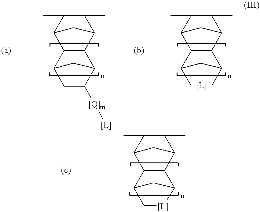
- the cyclic olefin units ii) contain lactone moiety which is (a) fused to a ring of the cyclic olefin—see structure III(b) below, (b) spiro-bonded to a ring of the cyclic olefin (such that at least one member of the spirolactone ring is also a member of a ring of the cyclic olefin)—see structure III(c) below, (c) bonded directly to a ring of the cyclic olefin without any atoms being shared between the lactone ring and a ring of the cyclic olefin—see structure III(a) below where m is zero, or (d) bonded to the cyclic olefin through a hydrocarbon moiety—see structure III(a) below where m is at least one.
- the lactone moiety contains a 5 to 7 atom ring (including any atom(s) shared with the cyclic olefin ring), most preferably a 5 or 6 atom ring. More preferably, the lactone moiety is a spirolactone moiety (such that at least one member of the spirolactone ring is also a member of a ring of the cyclic olefin). Where the cyclic olefin monomeric unit containing the lactone moiety is capable of assuming different isomeric forms, it should be understood that the invention is not limited to any specific isomeric form and that mixtures of isomers can be used.
- cyclic olefin units ii) may be represented by structures III(a)-(c) below:
- [L] represents a lactone moiety
- [Q] is a hydrocarbon (preferably a C 1 -C 10 hydrocarbon, more preferably C 1 -C 3 )
- m is zero or a positive integer (preferably m is 0 or 1)
- n is zero or some positive integer (preferably n is 0 or 1).
- structures IV (a)-(c) below:
- 5-member or 6-member spirolactone rings are more preferred (e.g., such as structures IV(a) or (b) above).
- the cyclic olefin polymer may optionally further contain cyclic olefin units iii) which may be any cyclic olefin monomeric unit having an acidic polar functional group that promotes alkaline solubility.
- cyclic olefin monomers include the following monomers illustrated by structure (V) below where R 2 represents an acidic polar moiety and n is zero or some positive integer (preferably n is 0 or 1):
- cyclic olefin units iii) are selected from:
- R 2 represents an acidic polar moiety which promotes solubility in aqueous alkaline solutions.
- the acidic polar moieties preferably have a pK a of about 13 or less.
- Preferred acidic polar moieties contain polar groups selected from the group consisting of carboxyl, sulfonamidyl, fluoroalcohol, and other acidic polar groups.
- Preferred acidic polar moieties are carboxyl groups. If desired, combinations of cyclic olefin units iii) having differing acidic polar functional groups may be used.
- the cyclic olefin polymers of invention preferably comprise at least about 30 mole % of cyclic olefin units i), more preferably about 50-95 mole %, most preferably about 60-85 mole %.
- the cyclic olefin polymer further contains optional cyclic olefin monomer iii)
- the amount of cyclic olefin monomer i) is preferably about 40-75 mole %, more preferably about 50-70 mole %.
- the cyclic olefin polymers of the invention preferably contain at least about 5 mole % of cyclic olefin monomer ii), more preferably about 5-50 mole %, most preferably about 15-40 mole %.
- the cyclic olefin polymer further contains optional cyclic olefin monomer iii)
- the amount of cyclic olefin monomer ii) is preferably about 10-50 mole %, more preferably about 15-40 mole %.
- the cyclic olefin polymer of the invention contains cyclic olefin monomers iii), the cyclic olefin polymer preferably contains about 5-30 mole % of cyclic olefin units iii), more preferably about 5-15 mole %.
- the cyclic olefin polymers of the invention preferably consist essentially of cyclic olefin units i) and ii) or of cyclic olefin units i), ii) and iii).
- the cyclic olefin polymers of the invention preferably contain sufficient monomer i) such that the polymer itself is substantially insoluble in aqueous alkaline developers commonly used in lithographic applications.
- the photoresist compositions of the invention contain a photosensitive acid generator (PAG).
- PAG photosensitive acid generator
- the invention is not limited to the use of any specific PAG or combination of PAG's, that is the benefits of the invention may be achieved using various photosensitive acid generators known in the art.
- Preferred PAG's are those which contain reduced amounts (or preferably zero) aryl moieties. Where aryl-containing PAG is employed, the absorptive characteristics of the PAG at 193 nm may restrict the amount of PAG that can be included in the formulation.
- Suitable photosensitive acid generators include (but preferably with alkyl substituted for one or more of any indicated aryl moieties) onium salts such as triaryl sulfonium hexafluoroantimonate, diaryliodonium hexafluoroantimonate, hexafluoroarsenates, triflates, perfluoroalkane sulfonates (e.g., perfluoromethane sulfonate, perfluorobutane, perfluorohexane sulfonate, perfluorooctane sulfonate etc.), substituted aryl sulfonates such as pyrogallols (e.g.
- the photoresist compositions of the invention preferably further contain a bulky, hydrophobic additive (“BH” additives) which is substantially transparent to 193 nm radiation.
- BH additives have generally enable and/or enhance the ability to resolve ultrafine lithographic features in response to conventional aqueous alkaline developers.
- the BH additives are preferably characterized by the presence of at least one alicyclic moiety.
- the BH additive contains at least about 10 carbon atoms, more preferably at least 14 carbon atoms, most preferably about 14 to 60 carbon atoms.
- the BH additive preferably contains one or more additional moieties such as acid-labile pendant groups which undergo cleaving in the presence of acid to provide a constituent which acts to promote alkaline solubility of the radiation-exposed portions of the photoresist.
- Preferred BH additives are selected from the group consisting of saturated steroid compounds, non-steroidal alicyclic compounds, and non-steroidal multi-alicyclic compounds having plural acid-labile connecting groups between at least two alicyclic moieties. More preferred BH additives include lithocholates such as t-butyl-3-trifluoroacetyllithocholate, t-butyl adamantane carboxylate, and bis-adamantyl t-butyl carboxylate. Bis-adamantyl t-butyl carboxylate is a most preferred BH additive. If desired, a combination of BH additives can be used.
- the photoresist compositions of the invention will typically contain a solvent prior to their application to the desired substrate.
- the solvent may be any solvent conventionally used with acid-catalyzed photoresists which otherwise does not have any excessively adverse impact on the performance of the photoresist composition.
- Preferred solvents are propylene glycol monomethyl ether acetate, cyclohexanone, and ethyl cellosolve acetate.
- compositions of the invention may further contain minor amounts of auxiliary components such as dyes/sensitizers, base additives, etc. as are known in the art.
- Preferred base additives are weak bases which scavenge trace acids while not having an excessive impact on the performance of the photoresist.
- Preferred base additives are (aliphatic or alicyclic) tertiary alkyl amines or t-alkyl ammonium hydroxides such as t-butyl ammonium hydroxide (TBAH).
- the photoresist compositions of the invention preferably contain about 0.5-20 wt. % (more preferably about 3-15 wt. %) photosensitive acid generator based on the total weight of cyclic olefin polymer in the composition. Where a solvent is present, the overall composition preferably contains about 50-90 wt. % solvent. The composition preferably contains about 1 wt. % or less of said base additive based on the total weight of acid sensitive polymer. The photoresist compositions of the invention preferably contain at least about 5 wt. % of the BH additive component based on the total weight of cyclic olefin polymer in the composition, more preferably about 10-25 wt. %, most preferably about 10-20 wt. %.
- the lactone cyclic olefin monomers and other monomers used in the present invention may be synthesized by known techniques.
- the spirolactone-functionalized monomers can be synthesized by Diels-Adler reaction with a-methylene butyrolactone and cyclic olefin (e.g., norbornene). This type of reaction is disclosed by Fotiadu et al., Tetrahedron Letters , 1990, 31, 4863-4866.
- the desired lactone-functionalized monomers can be prepared using processes described by Hasloin et al., Tetrahedron Letters , 1976, 4651 and Kayser et al., Can. J. Chem. 1978, 56,1524.
- the invention is not limited to any specific method of synthesizing the cyclic olefin polymers used in the invention.
- the cyclic olefin polymers are formed by addition polymerization. Examples of suitable techniques are disclosed in U.S. Pat. Nos. 5,468,819 and 5,705,503 assigned to B. F. Goodrich Company, the disclosures of which are incorporated herein by reference.
- the cyclic olefin polymers of the invention preferably have a weight average molecular weight of about 5,000-100,000, more preferably about 10,000-50,000.
- the photoresist compositions of the invention can be prepared by combining the cyclic olefin polymer, PAG, optional BH additive and any other desired ingredients using conventional methods.
- the photoresist composition to be used in photolithographic processes will generally have a significant amount of solvent.
- the photoresist compositions of the invention are especially useful for photolithographic processes used in the manufacture of integrated circuits on semiconductor substrates.
- the compositions are especially useful for photolithographic processes using 193 nm UV radiation. Where use of other radiation (e.g. mid-UV, 248 nm deep UV, x-ray, or e-beam) is desired, the compositions of the invention can be adjusted (if necessary) by the addition of an appropriate dye or sensitizer to the composition.
- the general use of the photoresist compositions of the invention in photolithography for semiconductors is described below.
- Semiconductor photolithographic applications generally involve transfer of a pattern to a layer of material on the semiconductor substrate.
- the material layer of the semiconductor substrate may be a metal conductor layer, a ceramic insulator layer, a semiconductor layer or other material depending on the stage of the manufacture process and the desired material set for the end product.
- an antireflective coating is applied over the material layer before application of the photoresist layer.
- the ARC layer may be any conventional ARC which is compatible with acid catalyzed photoresists.
- the solvent-containing photoresist composition is applied to the desired semiconductor substrate using spin coating or other technique.
- the substrate with the photoresist coating is then preferably heated (pre-exposure baked) to remove the solvent and improve the coherence of the photoresist layer.
- the thickness of the applied layer is preferably as thin as possible with the provisos that the thickness is preferably substantially uniform and that the photoresist layer be sufficient to withstand subsequent processing (typically reactive ion etching) to transfer the lithographic pattern to the underlying substrate material layer.
- the pre-exposure bake step is preferably conducted for about 10 seconds to 15 minutes, more preferably about 15 seconds to one minute.
- the pre-exposure bake temperature may vary depending on the glass transition temperature of the photoresist.
- the pre-exposure bake is performed at temperatures which are at least 20° C. below T g .
- the photoresist layer is then patternwise-exposed to the desired radiation (e.g. 193 nm ultraviolet radiation).
- the desired radiation e.g. 193 nm ultraviolet radiation
- patternwise exposure may be achieved by scanning the beam across the substrate and selectively applying the beam in the desired pattern. More typically, where wavelike radiation forms such as 193 nm ultraviolet radiation, the patternwise exposure is conducted through a mask which is placed over the photoresist layer.
- the total exposure energy is preferably about 100 millijoules/cm 2 or less, more preferably about 50 millijoules/cm 2 or less (e.g. 15-30 .millijoules/cm 2 ).
- the photoresist layer is typically baked to further complete the acid-catalyzed reaction and to enhance the contrast of the exposed pattern.
- the post-exposure bake is preferably conducted at about 100-175° C., more preferably about 125-160° C.
- the post-exposure bake is preferably conducted for about 30 seconds to 5 minutes.
- the photoresist structure with the desired pattern is obtained (developed) by contacting the photoresist layer with an alkaline solution which selectively dissolves the areas of the photoresist which were exposed to radiation.
- alkaline solutions are aqueous solutions of tetramethyl ammonium hydroxide.
- the photoresist compositions of the invention can be developed with conventional 0.26N aqueous alkaline solutions.
- the photoresist compositions of the invention can also be developed using 0.14N or 0.21N or other aqueous alkaline solutions.
- the resulting photoresist structure on the substrate is then typically dried to remove any remaining developer solvent.
- the photoresist compositions of the invention are generally characterized in that the product photoresist structures have high etch resistance. In some instances, it may be possible to further enhance the etch resistance of the photoresist structure by using a post-silylation technique using methods known in the art.
- the compositions of the invention enable the reproduction of lithographic features.
- the pattern from the photoresist structure may then be transferred to the material (e.g., ceramic, metal or semiconductor) of the underlying substrate.
- the transfer is achieved by reactive ion etching or some other etching technique.
- the etch resistance of the photoresist layer is especially important.
- the compositions of the invention and resulting photoresist structures can be used to create patterned material layer structures such as metal wiring lines, holes for contacts or vias, insulation sections (e.g., damascene trenches or shallow trench isolation), trenches for capacitor structures, etc. as might be used in the design of integrated circuit devices.
- the processes for making these (ceramic, metal or semiconductor) features generally involve providing a material layer or section of the substrate to be patterned, applying a layer of photoresist over the material layer or section, patternwise exposing the photoresist to radiation, developing the pattern by contacting the exposed photoresist with a solvent, etching the layer(s) underlying the photoresist layer at spaces in the pattern whereby a patterned material layer or substrate section is formed, and removing any remaining photoresist from the substrate.
- a hard mask may be used below the photoresist layer to facilitate transfer of the pattern to a further underlying material layer or section. Examples of such processes are disclosed in U.S. Pat. Nos.
- a terpolymer containing approximately 20 mole % norbornene spirolactone (as a mixture of isomers), 70 mole % norbornene carboxylic acid t-butyl ester, and 10 mole % norbornene carboxylic acid was prepared by addition polymerization.
- a solution (10% polymer by weight) of the polymer described in Example 1 was prepared in a mixture (80:20 by weight) of propylene glycol methyl ether acetate and ⁇ -butyrolactone. To this solution was added 4% (based on the weight of polymer) bis-(t-butylphenyl)iodonium perfluorooctanesulfonate, and 1.2% (based on weight of polymer) of a 1 M solution of tetra(n-butyl)ammmonium hydroxide in methanol.
- the solution was spin-cast onto a silicon wafer prepared with a commercially available anti-reflective coating, and baked at 130° C. for 60 s.
- the film thickness was approximately 4000 A.
- the film was exposed to patterned 193 nm radiation using an ISI ArF Microstepper, then baked at 150° C. for 90 s.
- the film was developed using a commercially available 0.262 N TMAH developer for 60 s, then rinsed and dried. Inspection with optical and scanning electron microscopy revealed fine features to dimensions approaching 0.25 ⁇ m at doses ranging from 40-50 mJ/cm 2 .
- a solution (10% polymer by weight) of the polymer described in Example 1 was prepared in propylene glycol methyl ether acetate. To this solution was added 15% (based on the weight of polymer) t-butyl lithocholate, 4% (based on the weight of polymer) bis-(t-butylphenyl)iodonium perfluorooctanesulfonate, and 1.2% (based on weight of polymer) of a 1 M solution of tetra(n-butyl)ammmonium hydroxide in methanol.
- the solution was spin-cast onto a silicon wafer prepared with a commercially available anti-reflective coating, and baked at 130° C. for 60 s.
- the film thickness was approximately 4000 A.
- the film was exposed to patterned 193 nm radiation using an ISI ArF Microstepper, then baked at 150° C. for 90 s.
- the film was developed using a commercially available 0.262 N TMAH developer for 60 s, then rinsed and dried. Inspection with optical and scanning electron microscopy revealed fine features to dimensions approaching 0.18 ⁇ m at doses ranging from 40-50 mJ/cm 2 .
- a solution (10% polymer by weight) of the polymer described in Example 1 was prepared in propylene glycol methyl ether acetate. To this solution was added 15% (based on the weight of polymer) 2,5-bis(adamantanoyloxy)-2,5-dimethylbutane, 4% (based on the weight of polymer) bis-(t-butylphenyl)iodonium perfluorooctanesulfonate, and 1.2% (based on weight of polymer) of a 1 M solution of tetra(n-butyl)ammmonium hydroxide in methanol.
- the solution was spin-cast onto a silicon wafer prepared with a commercially available anti-reflective coating, and baked at 130° C. for 60 s.
- the film thickness was approximately 4000 A.
- the film was exposed to patterned 193 nm radiation using an ISI ArF Microstepper, then baked at 150° C. for 90 s.
- the film was developed using a commercially available 0.262 N TMAH developer for 60 s, then rinsed and dried. Inspection with optical and scanning electron microscopy revealed fine features to dimensions approaching 0.15 ⁇ m at doses ranging from 40-50 mJ/cm 2 .
Abstract
Description


Claims (31)
Priority Applications (6)
| Application Number | Priority Date | Filing Date | Title |
|---|---|---|---|
| US09/566,395 US6251560B1 (en) | 2000-05-05 | 2000-05-05 | Photoresist compositions with cyclic olefin polymers having lactone moiety |
| TW090107609A TW588219B (en) | 2000-05-05 | 2001-03-30 | Photoresist compositions with cyclic olefin polymers having lactone moiety |
| KR10-2001-0018124A KR100487205B1 (en) | 2000-05-05 | 2001-04-06 | Photoresist compositions with cyclic olefin polymers having lactone moiety |
| DE10118902A DE10118902A1 (en) | 2000-05-05 | 2001-04-18 | Cyclic olefin polymer photoresist compositions containing lactone |
| JP2001130763A JP3418184B2 (en) | 2000-05-05 | 2001-04-27 | Photoresist composition having cyclic olefin polymer having lactone moiety |
| CNB011171588A CN1189792C (en) | 2000-05-05 | 2001-04-27 | Photoresist composition containing cycloolefine polymer with lactone part |
Applications Claiming Priority (1)
| Application Number | Priority Date | Filing Date | Title |
|---|---|---|---|
| US09/566,395 US6251560B1 (en) | 2000-05-05 | 2000-05-05 | Photoresist compositions with cyclic olefin polymers having lactone moiety |
Publications (1)
| Publication Number | Publication Date |
|---|---|
| US6251560B1 true US6251560B1 (en) | 2001-06-26 |
Family
ID=24262710
Family Applications (1)
| Application Number | Title | Priority Date | Filing Date |
|---|---|---|---|
| US09/566,395 Expired - Lifetime US6251560B1 (en) | 2000-05-05 | 2000-05-05 | Photoresist compositions with cyclic olefin polymers having lactone moiety |
Country Status (6)
| Country | Link |
|---|---|
| US (1) | US6251560B1 (en) |
| JP (1) | JP3418184B2 (en) |
| KR (1) | KR100487205B1 (en) |
| CN (1) | CN1189792C (en) |
| DE (1) | DE10118902A1 (en) |
| TW (1) | TW588219B (en) |
Cited By (14)
| Publication number | Priority date | Publication date | Assignee | Title |
|---|---|---|---|---|
| US20020132185A1 (en) * | 2000-05-05 | 2002-09-19 | International Business Machines Corporation | Copolymer photoresist with improved etch resistance |
| US6503687B2 (en) * | 1999-12-08 | 2003-01-07 | Samsung Electronics Co., Ltd. | Alicyclic photosensitive polymer, resist composition containing the same and method of preparing the resist composition |
| US6599677B2 (en) * | 2000-02-24 | 2003-07-29 | Shipley Company, L.L.C. | Polymer and photoresist compositions |
| US6627391B1 (en) * | 2000-08-16 | 2003-09-30 | International Business Machines Corporation | Resist compositions containing lactone additives |
| US20030211734A1 (en) * | 2000-07-07 | 2003-11-13 | Katsumi Maeda | Resist resin, chemical amplification type resist, and method of forming of pattern with the same |
| US6677419B1 (en) | 2002-11-13 | 2004-01-13 | International Business Machines Corporation | Preparation of copolymers |
| US6753124B2 (en) * | 2000-06-09 | 2004-06-22 | Jsr Corporation | Radiation-sensitive resin composition |
| US6756180B2 (en) | 2002-10-22 | 2004-06-29 | International Business Machines Corporation | Cyclic olefin-based resist compositions having improved image stability |
| US20040131968A1 (en) * | 1996-12-21 | 2004-07-08 | Hyundai Electronics Industries Co., Ltd. | Novel ArF photoresist copolymers |
| US6764811B2 (en) * | 2001-03-28 | 2004-07-20 | Matsushita Electric Industry Co., Ltd. | Pattern formation method |
| US6794109B2 (en) | 2001-02-23 | 2004-09-21 | Massachusetts Institute Of Technology | Low abosorbing resists for 157 nm lithography |
| US6936398B2 (en) * | 2001-05-09 | 2005-08-30 | Massachusetts Institute Of Technology | Resist with reduced line edge roughness |
| US20100305308A1 (en) * | 2002-04-03 | 2010-12-02 | Fonterra Corporate Research and Development Ltd. | Lactoferrin |
| CN111123643A (en) * | 2018-10-31 | 2020-05-08 | 台湾积体电路制造股份有限公司 | Protective composition and method for forming photoresist pattern |
Families Citing this family (5)
| Publication number | Priority date | Publication date | Assignee | Title |
|---|---|---|---|---|
| JP4831278B2 (en) * | 2000-09-14 | 2011-12-07 | 信越化学工業株式会社 | Polymer compound, resist material, and pattern forming method |
| US7611758B2 (en) * | 2003-11-06 | 2009-11-03 | Tokyo Electron Limited | Method of improving post-develop photoresist profile on a deposited dielectric film |
| US20070117040A1 (en) * | 2005-11-21 | 2007-05-24 | International Business Machines Corporation | Water castable-water strippable top coats for 193 nm immersion lithography |
| KR100669038B1 (en) * | 2006-01-18 | 2007-01-16 | 금호석유화학 주식회사 | Polymer containing norbornene derivatives having lactonyl and secondary hydroxyl group as repeating unit, and chemically amplified resist composition containing it |
| WO2019013793A1 (en) | 2017-07-13 | 2019-01-17 | Hewlett-Packard Development Company, L.P. | Coating composition(s) |
Citations (31)
| Publication number | Priority date | Publication date | Assignee | Title |
|---|---|---|---|---|
| US4400461A (en) | 1981-05-22 | 1983-08-23 | Bell Telephone Laboratories, Incorporated | Process of making semiconductor devices using photosensitive bodies |
| US4855017A (en) | 1985-05-03 | 1989-08-08 | Texas Instruments Incorporated | Trench etch process for a single-wafer RIE dry etch reactor |
| US5310619A (en) | 1986-06-13 | 1994-05-10 | Microsi, Inc. | Resist compositions comprising a phenolic resin, an acid forming onium salt and a tert-butyl ester or tert-butyl carbonate which is acid-cleavable |
| US5362663A (en) | 1992-01-09 | 1994-11-08 | International Business Machines Corporation | Method of forming double well substrate plate trench DRAM cell array |
| US5399647A (en) | 1992-06-10 | 1995-03-21 | Fujitsu Limited | Photoresist composition of 1-(1'-cyanoethenyl)adamantane |
| US5429710A (en) | 1993-02-25 | 1995-07-04 | Sony Corporation | Dry etching method |
| US5468819A (en) | 1993-11-16 | 1995-11-21 | The B.F. Goodrich Company | Process for making polymers containing a norbornene repeating unit by addition polymerization using an organo (nickel or palladium) complex |
| US5562801A (en) | 1994-04-28 | 1996-10-08 | Cypress Semiconductor Corporation | Method of etching an oxide layer |
| US5580694A (en) | 1994-06-27 | 1996-12-03 | International Business Machines Corporation | Photoresist composition with androstane and process for its use |
| US5585219A (en) | 1991-09-19 | 1996-12-17 | Fujitsu Limited | Resist composition and process for forming resist pattern |
| US5618751A (en) | 1996-05-23 | 1997-04-08 | International Business Machines Corporation | Method of making single-step trenches using resist fill and recess |
| WO1997033198A1 (en) | 1996-03-07 | 1997-09-12 | The B.F. Goodrich Company | Photoresist compositions comprising polycyclic polymers with acid labile pendant groups |
| US5705503A (en) | 1995-05-25 | 1998-01-06 | Goodall; Brian Leslie | Addition polymers of polycycloolefins containing functional substituents |
| US5738975A (en) | 1993-12-28 | 1998-04-14 | Nec Corporation | Photosensitive resin and method for patterning by use of the same |
| US5744376A (en) | 1996-04-08 | 1998-04-28 | Chartered Semiconductor Manufacturing Pte, Ltd | Method of manufacturing copper interconnect with top barrier layer |
| US5750680A (en) | 1995-09-14 | 1998-05-12 | Hyundai Electronics Industries Co., Ltd. | N-vinyllactam derivatives and polymer thereof |
| US5770346A (en) | 1995-12-11 | 1998-06-23 | Nec Corporation | Photoresist and compounds for composing the photoresist |
| US5776657A (en) | 1995-03-15 | 1998-07-07 | Ocg Microelectronic Materials, Inc. | Wet-chemical developable, etch-stable photoresist for UV radiation with a wavelength below 200 NM |
| US5801094A (en) | 1997-02-28 | 1998-09-01 | United Microelectronics Corporation | Dual damascene process |
| JPH10239845A (en) | 1997-02-25 | 1998-09-11 | Nec Corp | Photosensitive resin composition and pattern forming method |
| US5821469A (en) | 1996-12-18 | 1998-10-13 | Lucent Technologies Inc. | Device for securing cables in a telecommunications system |
| US5830965A (en) | 1994-02-01 | 1998-11-03 | Asahi Kasei Kogyo Kabushiki Kaisha | Polymer containing a modified cyclic monomer unit |
| JPH10301283A (en) | 1997-04-28 | 1998-11-13 | Toshiba Corp | Photosensitive composition and pattern forming method using the same |
| US5837419A (en) | 1995-08-31 | 1998-11-17 | Kabushiki Kaisha Toshiba | Photosensitive composition |
| EP0880074A1 (en) | 1997-03-07 | 1998-11-25 | Lucent Technologies Inc. | An energy-sensitive resist material and a process for device fabrication using an energy-sensitive resist material |
| US5843624A (en) | 1996-03-08 | 1998-12-01 | Lucent Technologies Inc. | Energy-sensitive resist material and a process for device fabrication using an energy-sensitive resist material |
| US6048664A (en) | 1999-03-12 | 2000-04-11 | Lucent Technologies, Inc. | Energy-sensitive resist material and a process for device fabrication using an energy-sensitive resist material |
| US6103449A (en) * | 1998-02-03 | 2000-08-15 | Fuji Photo Film Co., Ltd. | Negative working photoresist composition |
| US6103445A (en) * | 1997-03-07 | 2000-08-15 | Board Of Regents, The University Of Texas System | Photoresist compositions comprising norbornene derivative polymers with acid labile groups |
| US6124074A (en) * | 1999-03-11 | 2000-09-26 | International Business Machines Corporation | Photoresist compositions with cyclic olefin polymers and hydrophobic non-steroidal multi-alicyclic additives |
| US6156486A (en) * | 1997-08-05 | 2000-12-05 | Hitachi, Ltd. | Method for pattern formation and process for preparing semiconductor device |
Family Cites Families (5)
| Publication number | Priority date | Publication date | Assignee | Title |
|---|---|---|---|---|
| JPH10218941A (en) * | 1997-02-05 | 1998-08-18 | Oki Electric Ind Co Ltd | Resist resin, chemical amplification resist, and pattern formation method |
| JP3676918B2 (en) * | 1997-10-09 | 2005-07-27 | 富士通株式会社 | Resist material and resist pattern forming method |
| JP2000047387A (en) * | 1998-07-28 | 2000-02-18 | Fuji Photo Film Co Ltd | Positive type photoresist composition for exposure with far ultraviolet ray |
| JP3821961B2 (en) * | 1998-09-25 | 2006-09-13 | 株式会社ルネサステクノロジ | Pattern forming method, semiconductor device manufacturing method, and radiation-sensitive composition |
| KR100445920B1 (en) * | 1999-03-11 | 2004-08-25 | 인터내셔널 비지네스 머신즈 코포레이션 | Photoresist compositions with cyclic olefin polymers and additive |
-
2000
- 2000-05-05 US US09/566,395 patent/US6251560B1/en not_active Expired - Lifetime
-
2001
- 2001-03-30 TW TW090107609A patent/TW588219B/en not_active IP Right Cessation
- 2001-04-06 KR KR10-2001-0018124A patent/KR100487205B1/en not_active IP Right Cessation
- 2001-04-18 DE DE10118902A patent/DE10118902A1/en not_active Ceased
- 2001-04-27 CN CNB011171588A patent/CN1189792C/en not_active Expired - Fee Related
- 2001-04-27 JP JP2001130763A patent/JP3418184B2/en not_active Expired - Fee Related
Patent Citations (33)
| Publication number | Priority date | Publication date | Assignee | Title |
|---|---|---|---|---|
| US4400461A (en) | 1981-05-22 | 1983-08-23 | Bell Telephone Laboratories, Incorporated | Process of making semiconductor devices using photosensitive bodies |
| US4855017A (en) | 1985-05-03 | 1989-08-08 | Texas Instruments Incorporated | Trench etch process for a single-wafer RIE dry etch reactor |
| US5310619A (en) | 1986-06-13 | 1994-05-10 | Microsi, Inc. | Resist compositions comprising a phenolic resin, an acid forming onium salt and a tert-butyl ester or tert-butyl carbonate which is acid-cleavable |
| US5585219A (en) | 1991-09-19 | 1996-12-17 | Fujitsu Limited | Resist composition and process for forming resist pattern |
| US5362663A (en) | 1992-01-09 | 1994-11-08 | International Business Machines Corporation | Method of forming double well substrate plate trench DRAM cell array |
| US5399647A (en) | 1992-06-10 | 1995-03-21 | Fujitsu Limited | Photoresist composition of 1-(1'-cyanoethenyl)adamantane |
| US5429710A (en) | 1993-02-25 | 1995-07-04 | Sony Corporation | Dry etching method |
| US5468819A (en) | 1993-11-16 | 1995-11-21 | The B.F. Goodrich Company | Process for making polymers containing a norbornene repeating unit by addition polymerization using an organo (nickel or palladium) complex |
| US5738975A (en) | 1993-12-28 | 1998-04-14 | Nec Corporation | Photosensitive resin and method for patterning by use of the same |
| US5830965A (en) | 1994-02-01 | 1998-11-03 | Asahi Kasei Kogyo Kabushiki Kaisha | Polymer containing a modified cyclic monomer unit |
| US5562801A (en) | 1994-04-28 | 1996-10-08 | Cypress Semiconductor Corporation | Method of etching an oxide layer |
| US5580694A (en) | 1994-06-27 | 1996-12-03 | International Business Machines Corporation | Photoresist composition with androstane and process for its use |
| US5786131A (en) | 1994-06-27 | 1998-07-28 | International Business Machines Corporation | Process for use of photoresist composition with deep ultraviolet radiation |
| US5776657A (en) | 1995-03-15 | 1998-07-07 | Ocg Microelectronic Materials, Inc. | Wet-chemical developable, etch-stable photoresist for UV radiation with a wavelength below 200 NM |
| US5705503A (en) | 1995-05-25 | 1998-01-06 | Goodall; Brian Leslie | Addition polymers of polycycloolefins containing functional substituents |
| US5837419A (en) | 1995-08-31 | 1998-11-17 | Kabushiki Kaisha Toshiba | Photosensitive composition |
| US5750680A (en) | 1995-09-14 | 1998-05-12 | Hyundai Electronics Industries Co., Ltd. | N-vinyllactam derivatives and polymer thereof |
| US5770346A (en) | 1995-12-11 | 1998-06-23 | Nec Corporation | Photoresist and compounds for composing the photoresist |
| US6136499A (en) * | 1996-03-07 | 2000-10-24 | The B. F. Goodrich Company | Photoresist compositions comprising polycyclic polymers with acid labile pendant groups |
| WO1997033198A1 (en) | 1996-03-07 | 1997-09-12 | The B.F. Goodrich Company | Photoresist compositions comprising polycyclic polymers with acid labile pendant groups |
| US5843624A (en) | 1996-03-08 | 1998-12-01 | Lucent Technologies Inc. | Energy-sensitive resist material and a process for device fabrication using an energy-sensitive resist material |
| US5744376A (en) | 1996-04-08 | 1998-04-28 | Chartered Semiconductor Manufacturing Pte, Ltd | Method of manufacturing copper interconnect with top barrier layer |
| US5618751A (en) | 1996-05-23 | 1997-04-08 | International Business Machines Corporation | Method of making single-step trenches using resist fill and recess |
| US5821469A (en) | 1996-12-18 | 1998-10-13 | Lucent Technologies Inc. | Device for securing cables in a telecommunications system |
| JPH10239845A (en) | 1997-02-25 | 1998-09-11 | Nec Corp | Photosensitive resin composition and pattern forming method |
| US5801094A (en) | 1997-02-28 | 1998-09-01 | United Microelectronics Corporation | Dual damascene process |
| EP0880074A1 (en) | 1997-03-07 | 1998-11-25 | Lucent Technologies Inc. | An energy-sensitive resist material and a process for device fabrication using an energy-sensitive resist material |
| US6103445A (en) * | 1997-03-07 | 2000-08-15 | Board Of Regents, The University Of Texas System | Photoresist compositions comprising norbornene derivative polymers with acid labile groups |
| JPH10301283A (en) | 1997-04-28 | 1998-11-13 | Toshiba Corp | Photosensitive composition and pattern forming method using the same |
| US6156486A (en) * | 1997-08-05 | 2000-12-05 | Hitachi, Ltd. | Method for pattern formation and process for preparing semiconductor device |
| US6103449A (en) * | 1998-02-03 | 2000-08-15 | Fuji Photo Film Co., Ltd. | Negative working photoresist composition |
| US6124074A (en) * | 1999-03-11 | 2000-09-26 | International Business Machines Corporation | Photoresist compositions with cyclic olefin polymers and hydrophobic non-steroidal multi-alicyclic additives |
| US6048664A (en) | 1999-03-12 | 2000-04-11 | Lucent Technologies, Inc. | Energy-sensitive resist material and a process for device fabrication using an energy-sensitive resist material |
Non-Patent Citations (1)
| Title |
|---|
| Uetani, Y. et al, SPIE vol. 3678, pt. 1, Mar. 1999, 510-517. * |
Cited By (20)
| Publication number | Priority date | Publication date | Assignee | Title |
|---|---|---|---|---|
| US20040131968A1 (en) * | 1996-12-21 | 2004-07-08 | Hyundai Electronics Industries Co., Ltd. | Novel ArF photoresist copolymers |
| US6808859B1 (en) * | 1996-12-31 | 2004-10-26 | Hyundai Electronics Industries Co., Ltd. | ArF photoresist copolymers |
| US6866984B2 (en) | 1996-12-31 | 2005-03-15 | Hyundai Electronics Industries Co., Ltd. | ArF photoresist copolymers |
| US6503687B2 (en) * | 1999-12-08 | 2003-01-07 | Samsung Electronics Co., Ltd. | Alicyclic photosensitive polymer, resist composition containing the same and method of preparing the resist composition |
| US6599677B2 (en) * | 2000-02-24 | 2003-07-29 | Shipley Company, L.L.C. | Polymer and photoresist compositions |
| US20050170278A1 (en) * | 2000-02-24 | 2005-08-04 | Szmanda Charles R. | Polymer and photoresist compositions |
| US7118847B2 (en) | 2000-02-24 | 2006-10-10 | Shipley Company Llc | Polymer and photoresist compositions |
| US20020132185A1 (en) * | 2000-05-05 | 2002-09-19 | International Business Machines Corporation | Copolymer photoresist with improved etch resistance |
| US6753124B2 (en) * | 2000-06-09 | 2004-06-22 | Jsr Corporation | Radiation-sensitive resin composition |
| US20030211734A1 (en) * | 2000-07-07 | 2003-11-13 | Katsumi Maeda | Resist resin, chemical amplification type resist, and method of forming of pattern with the same |
| US6924079B2 (en) * | 2000-07-07 | 2005-08-02 | Nec Corporation | Resist resin, chemical amplification type resist, and method of forming of pattern with the same |
| US6627391B1 (en) * | 2000-08-16 | 2003-09-30 | International Business Machines Corporation | Resist compositions containing lactone additives |
| US6794109B2 (en) | 2001-02-23 | 2004-09-21 | Massachusetts Institute Of Technology | Low abosorbing resists for 157 nm lithography |
| US6764811B2 (en) * | 2001-03-28 | 2004-07-20 | Matsushita Electric Industry Co., Ltd. | Pattern formation method |
| US6936398B2 (en) * | 2001-05-09 | 2005-08-30 | Massachusetts Institute Of Technology | Resist with reduced line edge roughness |
| US20100305308A1 (en) * | 2002-04-03 | 2010-12-02 | Fonterra Corporate Research and Development Ltd. | Lactoferrin |
| US6756180B2 (en) | 2002-10-22 | 2004-06-29 | International Business Machines Corporation | Cyclic olefin-based resist compositions having improved image stability |
| US6677419B1 (en) | 2002-11-13 | 2004-01-13 | International Business Machines Corporation | Preparation of copolymers |
| CN111123643A (en) * | 2018-10-31 | 2020-05-08 | 台湾积体电路制造股份有限公司 | Protective composition and method for forming photoresist pattern |
| CN111123643B (en) * | 2018-10-31 | 2023-11-07 | 台湾积体电路制造股份有限公司 | Protective composition and method for forming photoresist pattern |
Also Published As
| Publication number | Publication date |
|---|---|
| CN1189792C (en) | 2005-02-16 |
| TW588219B (en) | 2004-05-21 |
| JP3418184B2 (en) | 2003-06-16 |
| KR100487205B1 (en) | 2005-05-04 |
| CN1322967A (en) | 2001-11-21 |
| JP2002014472A (en) | 2002-01-18 |
| DE10118902A1 (en) | 2002-03-14 |
| KR20010102848A (en) | 2001-11-16 |
Similar Documents
| Publication | Publication Date | Title |
|---|---|---|
| US6251560B1 (en) | Photoresist compositions with cyclic olefin polymers having lactone moiety | |
| US7129016B2 (en) | Positive resist containing naphthol functionality | |
| TWI533089B (en) | Photoresist composition for negative development and pattern forming method using thereof | |
| US6562554B1 (en) | Photoresist compositions with cyclic olefin polymers and hydrophobic non-steroidal multi-alicyclic additives | |
| US7087356B2 (en) | 193nm resist with improved post-exposure properties | |
| US6627391B1 (en) | Resist compositions containing lactone additives | |
| US6534239B2 (en) | Resist compositions with polymers having pendant groups containing plural acid labile moieties | |
| US6756180B2 (en) | Cyclic olefin-based resist compositions having improved image stability | |
| IL167255A (en) | Low silicon-outgassing resist for bilayer lithography | |
| JP3120402B2 (en) | Photoresist composition containing passivated aromatic amine compound | |
| US6635401B2 (en) | Resist compositions with polymers having 2-cyano acrylic monomer | |
| US7183036B2 (en) | Low activation energy positive resist | |
| US6391521B1 (en) | Resist compositions containing bulky anhydride additives | |
| US6265134B1 (en) | Photoresist compositions with pendant polar-functionalized aromatic groups and acid-labile branching | |
| KR100445920B1 (en) | Photoresist compositions with cyclic olefin polymers and additive | |
| US6770418B2 (en) | Positive resist compositions containing non-polymeric silicon | |
| JP3470967B2 (en) | Copolymer photoresists with improved etch resistance | |
| EP1716450A1 (en) | Use of mixed bases to enhance patterned resist profiles on chrome or sensitive substrates |
Legal Events
| Date | Code | Title | Description |
|---|---|---|---|
| AS | Assignment |
Owner name: INTERNATIONAL BUSINESS MACHINES CORPORATION, NEW Y Free format text: ASSIGNMENT OF ASSIGNORS INTEREST;ASSIGNORS:WALLOW, THOMAS I.;ALLEN, ROBERT D.;BROCK, PHILLIP JOE;AND OTHERS;REEL/FRAME:010997/0596;SIGNING DATES FROM 20000613 TO 20000707 |
|
| STCF | Information on status: patent grant |
Free format text: PATENTED CASE |
|
| FEPP | Fee payment procedure |
Free format text: PAYOR NUMBER ASSIGNED (ORIGINAL EVENT CODE: ASPN); ENTITY STATUS OF PATENT OWNER: LARGE ENTITY |
|
| FPAY | Fee payment |
Year of fee payment: 4 |
|
| FPAY | Fee payment |
Year of fee payment: 8 |
|
| REMI | Maintenance fee reminder mailed | ||
| FPAY | Fee payment |
Year of fee payment: 12 |
|
| SULP | Surcharge for late payment |
Year of fee payment: 11 |
|
| AS | Assignment |
Owner name: GLOBALFOUNDRIES U.S. 2 LLC, NEW YORK Free format text: ASSIGNMENT OF ASSIGNORS INTEREST;ASSIGNOR:INTERNATIONAL BUSINESS MACHINES CORPORATION;REEL/FRAME:036550/0001 Effective date: 20150629 |
|
| AS | Assignment |
Owner name: GLOBALFOUNDRIES INC., CAYMAN ISLANDS Free format text: ASSIGNMENT OF ASSIGNORS INTEREST;ASSIGNORS:GLOBALFOUNDRIES U.S. 2 LLC;GLOBALFOUNDRIES U.S. INC.;REEL/FRAME:036779/0001 Effective date: 20150910 |
|
| AS | Assignment |
Owner name: WILMINGTON TRUST, NATIONAL ASSOCIATION, DELAWARE Free format text: SECURITY AGREEMENT;ASSIGNOR:GLOBALFOUNDRIES INC.;REEL/FRAME:049490/0001 Effective date: 20181127 |
|
| AS | Assignment |
Owner name: GLOBALFOUNDRIES INC., CAYMAN ISLANDS Free format text: RELEASE BY SECURED PARTY;ASSIGNOR:WILMINGTON TRUST, NATIONAL ASSOCIATION;REEL/FRAME:054636/0001 Effective date: 20201117 |
|
| AS | Assignment |
Owner name: GLOBALFOUNDRIES U.S. INC., NEW YORK Free format text: RELEASE BY SECURED PARTY;ASSIGNOR:WILMINGTON TRUST, NATIONAL ASSOCIATION;REEL/FRAME:056987/0001 Effective date: 20201117 |