US6227869B1 - Terminal for an LGA socket - Google Patents
Terminal for an LGA socket Download PDFInfo
- Publication number
- US6227869B1 US6227869B1 US09/335,797 US33579799A US6227869B1 US 6227869 B1 US6227869 B1 US 6227869B1 US 33579799 A US33579799 A US 33579799A US 6227869 B1 US6227869 B1 US 6227869B1
- Authority
- US
- United States
- Prior art keywords
- arm
- terminal
- securing
- socket
- projection
- Prior art date
- Legal status (The legal status is an assumption and is not a legal conclusion. Google has not performed a legal analysis and makes no representation as to the accuracy of the status listed.)
- Expired - Fee Related
Links
Images


Classifications
-
- H—ELECTRICITY
- H05—ELECTRIC TECHNIQUES NOT OTHERWISE PROVIDED FOR
- H05K—PRINTED CIRCUITS; CASINGS OR CONSTRUCTIONAL DETAILS OF ELECTRIC APPARATUS; MANUFACTURE OF ASSEMBLAGES OF ELECTRICAL COMPONENTS
- H05K7/00—Constructional details common to different types of electric apparatus
- H05K7/02—Arrangements of circuit components or wiring on supporting structure
- H05K7/10—Plug-in assemblages of components, e.g. IC sockets
- H05K7/1053—Plug-in assemblages of components, e.g. IC sockets having interior leads
- H05K7/1061—Plug-in assemblages of components, e.g. IC sockets having interior leads co-operating by abutting
- H05K7/1069—Plug-in assemblages of components, e.g. IC sockets having interior leads co-operating by abutting with spring contact pieces
-
- H—ELECTRICITY
- H01—ELECTRIC ELEMENTS
- H01R—ELECTRICALLY-CONDUCTIVE CONNECTIONS; STRUCTURAL ASSOCIATIONS OF A PLURALITY OF MUTUALLY-INSULATED ELECTRICAL CONNECTING ELEMENTS; COUPLING DEVICES; CURRENT COLLECTORS
- H01R12/00—Structural associations of a plurality of mutually-insulated electrical connecting elements, specially adapted for printed circuits, e.g. printed circuit boards [PCB], flat or ribbon cables, or like generally planar structures, e.g. terminal strips, terminal blocks; Coupling devices specially adapted for printed circuits, flat or ribbon cables, or like generally planar structures; Terminals specially adapted for contact with, or insertion into, printed circuits, flat or ribbon cables, or like generally planar structures
- H01R12/50—Fixed connections
- H01R12/51—Fixed connections for rigid printed circuits or like structures
- H01R12/52—Fixed connections for rigid printed circuits or like structures connecting to other rigid printed circuits or like structures
-
- H—ELECTRICITY
- H01—ELECTRIC ELEMENTS
- H01R—ELECTRICALLY-CONDUCTIVE CONNECTIONS; STRUCTURAL ASSOCIATIONS OF A PLURALITY OF MUTUALLY-INSULATED ELECTRICAL CONNECTING ELEMENTS; COUPLING DEVICES; CURRENT COLLECTORS
- H01R12/00—Structural associations of a plurality of mutually-insulated electrical connecting elements, specially adapted for printed circuits, e.g. printed circuit boards [PCB], flat or ribbon cables, or like generally planar structures, e.g. terminal strips, terminal blocks; Coupling devices specially adapted for printed circuits, flat or ribbon cables, or like generally planar structures; Terminals specially adapted for contact with, or insertion into, printed circuits, flat or ribbon cables, or like generally planar structures
- H01R12/70—Coupling devices
- H01R12/7082—Coupling device supported only by cooperation with PCB
-
- H—ELECTRICITY
- H01—ELECTRIC ELEMENTS
- H01R—ELECTRICALLY-CONDUCTIVE CONNECTIONS; STRUCTURAL ASSOCIATIONS OF A PLURALITY OF MUTUALLY-INSULATED ELECTRICAL CONNECTING ELEMENTS; COUPLING DEVICES; CURRENT COLLECTORS
- H01R12/00—Structural associations of a plurality of mutually-insulated electrical connecting elements, specially adapted for printed circuits, e.g. printed circuit boards [PCB], flat or ribbon cables, or like generally planar structures, e.g. terminal strips, terminal blocks; Coupling devices specially adapted for printed circuits, flat or ribbon cables, or like generally planar structures; Terminals specially adapted for contact with, or insertion into, printed circuits, flat or ribbon cables, or like generally planar structures
- H01R12/50—Fixed connections
- H01R12/51—Fixed connections for rigid printed circuits or like structures
- H01R12/55—Fixed connections for rigid printed circuits or like structures characterised by the terminals
- H01R12/57—Fixed connections for rigid printed circuits or like structures characterised by the terminals surface mounting terminals
-
- H—ELECTRICITY
- H01—ELECTRIC ELEMENTS
- H01R—ELECTRICALLY-CONDUCTIVE CONNECTIONS; STRUCTURAL ASSOCIATIONS OF A PLURALITY OF MUTUALLY-INSULATED ELECTRICAL CONNECTING ELEMENTS; COUPLING DEVICES; CURRENT COLLECTORS
- H01R13/00—Details of coupling devices of the kinds covered by groups H01R12/70 or H01R24/00 - H01R33/00
- H01R13/02—Contact members
- H01R13/22—Contacts for co-operating by abutting
- H01R13/24—Contacts for co-operating by abutting resilient; resiliently-mounted
Definitions
- the present invention relates to an LGA socket, and particularly to a low profile LGA socket for reliably connecting a first printed circuit board and a second printed circuit board.
- a first object of the present invention is to provide an LGA socket having terminals which each have a short electrical path thereby reducing self-inductance effects.
- a second object of the present invention is to provide an LGA socket having a limited height.
- a third object of the present invention is to provide an LGA socket which has a plurality of terminals reliably retained therein.
- a fourth object of the present invention is to provide an LGA socket including a plurality of terminals having an adjustable height.
- an LGA socket of the present invention comprises an insulative housing defining a plurality of passageways therethrough and a corresponding number of terminals retained therein.
- Each terminal forms upper and lower spring arms partially extending beyond the corresponding passageway, a curved linking portion for connecting the upper and lower arms, and a securing arm extending upward from the lower arm towards the upper arm.
- Retaining means is formed on the securing arm for securing the terminal in the corresponding passageway.
- the retaining means comprises locking barbs formed on at least one side of the securing arm.
- the upper and lower arms engage electrical pads formed on a first circuit board and a second circuit board, respectively.
- the retaining means is a combination of a first projection extending from a recess of the securing arm and a second projection stamped from the securing arm.
- the first and second projections are adapted to abut against a protrusion projecting from an inner side of the passageway.
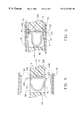
- FIG. 1 is a perspective view of a terminal in accordance with a first embodiment of the present invention
- FIG. 2 is a cross sectional view of an LGA socket before contacting a first circuit board and a second circuit board;
- FIG. 3 is an assembled view of FIG. 2;
- FIG. 4 is a perspective view of a terminal in accordance with a second embodiment of the present invention.
- FIG. 5 is a cross sectional view of an LGA socket before contacting a first circuit board and a second circuit board;
- FIG. 6 is an assembled view of FIG. 5;
- FIG. 7 is a perspective view of a terminal in accordance with a third embodiment of the present invention.
- FIG. 8 is a cross sectional view of an LGA socket before contacting a first circuit board and a second circuit board.
- FIG. 9 is an assembled view of FIG. 8 .
- an LGA socket includes an insulative housing 2 defining a plurality of passageways 20 therethrough and a corresponding number of D-shaped terminals 1 retained therein.
- Each terminal 1 forms upper and lower spring arms 10 , 11 which partially extend beyond the corresponding passageway 20 .
- the upper and lower arms 10 , 11 are connected by a curved linking portion 12 .
- a securing arm 13 extends upward from an end of the lower arm 11 towards the upper arm 10 .
- the upper arm 10 has a curved end 100 projecting up and extending beyond the passageway 20 .
- the lower arm 11 has a curved portion 110 opposite the curved end 100 .
- the securing arm 13 forms a recess 130 at an end thereof and retaining means for securing the terminal 1 in the passageway 20 .
- a slanted leading edge 132 is formed in the recess 130 of the securing arm 13 for guiding a downward movement of the upper arm 10 .
- the retaining means comprises locking barbs 131 formed on both sides of the securing arm 13 .
- the LGA socket is mounted on a second circuit board.
- the curved portion 110 of the terminal abuts against an electrical pad 31 of the second board.
- the curved end 100 of the terminal 1 abuts against an electrical pad 30 of the first board.
- the upper arm 10 of the terminal 1 is then deformed to contact the securing arm 13 thereby providing a short electrical path therethrough and reducing the overall height of the LGA socket.
- Such a short electrical path can effectively reduce self-inductance effects.
- the linking portion 12 is distant from an opposing side of the passageway 20 which provides the connecting portion 12 with clearance for movement.
- an LGA socket in accordance with a second embodiment of the present invention includes an insulative housing 5 defining a plurality of passageways 50 therethrough and a corresponding number of terminals 4 retained therein.
- Each terminal 4 is basically similar to the terminal 1 of the first embodiment and has an upper spring arm 40 forming a curved end 400 , a lower spring arm 41 having a curved portion 410 , a linking portion 42 , and a securing arm 43 with recess 430 defined therein.
- Retaining means formed on the securing arm 43 is a first projection 431 extending from the recess 430 and a second projection 432 stamped from the securing arm.
- the first and second projections 431 , 432 are adapted to abut against a protrusion 500 projecting from an inner side of the passageway 50 .
- a gap 6 is provided between the first projection 431 and the protrusion 500 such that the terminal 4 can be moveable in the passageway 50 in a vertical direction.
- both sides of the securing arm 43 are engaged with inner sides of the passageway 50 for retaining the terminal 4 in the passageway 50 .
- the LGA socket is mounted on a second circuit board.
- the curved portion 410 of the lower arm 41 abuts against an electrical pad 61 of the second board.
- the curved end 400 abuts against an electrical pad 60 of the board.
- the upper arm 40 of the terminal 4 is then deformed to contact the securing arm 43 thereby providing a short electrical path therethrough and reducing the overall height of the LGA socket. Such a short electrical path can effectively reduce self-inductance effects.
- an LGA socket in accordance with a third embodiment of the present invention includes an insulative housing 8 defining a plurality of passageways 80 therethrough and a corresponding number of terminals 7 retained therein.
- the terminal 7 is basically similar to the terminal 4 of the second embodiment and has an upper spring arm 70 forming a curved end 700 , a lower spring arm 71 , a linking portion 72 , and a securing arm 73 with a recess 730 defined therein and first and second projections 731 , 732 formed thereon.
- a tine portion 733 is stamped from the securing arm 73 adjacent to the lower arm 71 .
- a gap 92 is defined between the first projection 731 and a protrusion 800 projecting from an inner side of the passageway 80 .
- another gap 93 is defined between the second projection 732 and the protrusion 800 .
- the two gaps 92 , 93 provide the terminal 7 with an adjustable position, thus the terminal 7 can be moveable in the passageway 80 in a vertical direction.
- both sides of the securing arm 73 including the tine portion 733 , are engaged with corresponding inner sides of the passageway 80 for retaining the terminal 7 therein.
- the LGA socket is mounted on a second circuit board.
- the tine portion 722 of the terminal 7 abuts against an electrical pad 91 of the second board.
- the curved end 700 abuts against an electrical pad 90 of the first board.
- the upper arm 70 of the terminal 7 is then deformed to contact the securing arm 73 thereby providing a short electrical path therethrough and reducing the overall height of the LGA socket. Such a short electrical path can effectively reduce self-inductance effects.
Abstract
An LGA socket comprises an insulative housing defining a number of passageways therethrough and a corresponding number of terminals retained therein. Each terminal forms upper and lower spring arms partially extending beyond the corresponding passageway, a curved linking portion for connecting the upper and lower arms, and a securing arm extending from the lower arm towards the upper arm and secured to the insulative housing. The upper arm can be deformed to contact the securing arm thereby providing a short electrical path therethrough and reducing the overall height of the LGA socket.
Description
The present invention relates to an LGA socket, and particularly to a low profile LGA socket for reliably connecting a first printed circuit board and a second printed circuit board.
Personal computers, especially notebook computers, become increasingly compact and multifunctional. The components assembled therein, such as terminals for connecting a first circuit board and a second circuit board must be reliable and have a reduced dimension. U.S. Pat. Nos. 5,308,252 and 5,653,598 disclose pertinent terminal configurations. Each conventional terminal is received in a socket and has two spring arms projecting beyond an insulative housing of the socket for contacting corresponding portions of a first circuit board and a second circuit board, respectively. However, the terminals are retained at only one point of the socket and lack an adjustable height. Thus, the terminal is unreliable and susceptible to mechanical forces which may adversely affect signal transmission through the socket.
Accordingly, a first object of the present invention is to provide an LGA socket having terminals which each have a short electrical path thereby reducing self-inductance effects.
A second object of the present invention is to provide an LGA socket having a limited height.
A third object of the present invention is to provide an LGA socket which has a plurality of terminals reliably retained therein.
A fourth object of the present invention is to provide an LGA socket including a plurality of terminals having an adjustable height.
To fully accomplish the above-mentioned objects, an LGA socket of the present invention comprises an insulative housing defining a plurality of passageways therethrough and a corresponding number of terminals retained therein. Each terminal forms upper and lower spring arms partially extending beyond the corresponding passageway, a curved linking portion for connecting the upper and lower arms, and a securing arm extending upward from the lower arm towards the upper arm. Retaining means is formed on the securing arm for securing the terminal in the corresponding passageway. The retaining means comprises locking barbs formed on at least one side of the securing arm. In assembly, the upper and lower arms engage electrical pads formed on a first circuit board and a second circuit board, respectively. The upper arm is then deformed to contact the securing arm thereby providing a short electrical path therethrough for reducing self-inductance effects. Alternatively, the retaining means is a combination of a first projection extending from a recess of the securing arm and a second projection stamped from the securing arm. The first and second projections are adapted to abut against a protrusion projecting from an inner side of the passageway.
FIG. 1 is a perspective view of a terminal in accordance with a first embodiment of the present invention;
FIG. 2 is a cross sectional view of an LGA socket before contacting a first circuit board and a second circuit board;
FIG. 3 is an assembled view of FIG. 2;
FIG. 4 is a perspective view of a terminal in accordance with a second embodiment of the present invention;
FIG. 5 is a cross sectional view of an LGA socket before contacting a first circuit board and a second circuit board;
FIG. 6 is an assembled view of FIG. 5;
FIG. 7 is a perspective view of a terminal in accordance with a third embodiment of the present invention;
FIG. 8 is a cross sectional view of an LGA socket before contacting a first circuit board and a second circuit board; and
FIG. 9 is an assembled view of FIG. 8.
Referring to FIGS. 1 and 2, an LGA socket includes an insulative housing 2 defining a plurality of passageways 20 therethrough and a corresponding number of D-shaped terminals 1 retained therein. Each terminal 1 forms upper and lower spring arms 10, 11 which partially extend beyond the corresponding passageway 20. The upper and lower arms 10, 11 are connected by a curved linking portion 12. A securing arm 13 extends upward from an end of the lower arm 11 towards the upper arm 10.
The upper arm 10 has a curved end 100 projecting up and extending beyond the passageway 20. Correspondingly, the lower arm 11 has a curved portion 110 opposite the curved end 100. The securing arm 13 forms a recess 130 at an end thereof and retaining means for securing the terminal 1 in the passageway 20. A slanted leading edge 132 is formed in the recess 130 of the securing arm 13 for guiding a downward movement of the upper arm 10. The retaining means comprises locking barbs 131 formed on both sides of the securing arm 13.
Referring to FIG. 3, the LGA socket is mounted on a second circuit board. The curved portion 110 of the terminal abuts against an electrical pad 31 of the second board. When the socket engages with a first circuit board, the curved end 100 of the terminal 1 abuts against an electrical pad 30 of the first board. The upper arm 10 of the terminal 1 is then deformed to contact the securing arm 13 thereby providing a short electrical path therethrough and reducing the overall height of the LGA socket. Such a short electrical path can effectively reduce self-inductance effects. In addition, the linking portion 12 is distant from an opposing side of the passageway 20 which provides the connecting portion 12 with clearance for movement.
Referring to FIGS. 4 and 5, an LGA socket in accordance with a second embodiment of the present invention includes an insulative housing 5 defining a plurality of passageways 50 therethrough and a corresponding number of terminals 4 retained therein. Each terminal 4 is basically similar to the terminal 1 of the first embodiment and has an upper spring arm 40 forming a curved end 400, a lower spring arm 41 having a curved portion 410, a linking portion 42, and a securing arm 43 with recess 430 defined therein. Retaining means formed on the securing arm 43 is a first projection 431 extending from the recess 430 and a second projection 432 stamped from the securing arm. The first and second projections 431, 432 are adapted to abut against a protrusion 500 projecting from an inner side of the passageway 50. A gap 6 is provided between the first projection 431 and the protrusion 500 such that the terminal 4 can be moveable in the passageway 50 in a vertical direction. In addition, both sides of the securing arm 43 are engaged with inner sides of the passageway 50 for retaining the terminal 4 in the passageway 50.
Referring to FIG. 6, the LGA socket is mounted on a second circuit board. The curved portion 410 of the lower arm 41 abuts against an electrical pad 61 of the second board. When the socket engages with a first circuit board, the curved end 400 abuts against an electrical pad 60 of the board. The upper arm 40 of the terminal 4 is then deformed to contact the securing arm 43 thereby providing a short electrical path therethrough and reducing the overall height of the LGA socket. Such a short electrical path can effectively reduce self-inductance effects.
Referring to FIGS. 7 and 8, an LGA socket in accordance with a third embodiment of the present invention includes an insulative housing 8 defining a plurality of passageways 80 therethrough and a corresponding number of terminals 7 retained therein. The terminal 7 is basically similar to the terminal 4 of the second embodiment and has an upper spring arm 70 forming a curved end 700, a lower spring arm 71, a linking portion 72, and a securing arm 73 with a recess 730 defined therein and first and second projections 731, 732 formed thereon. A tine portion 733 is stamped from the securing arm 73 adjacent to the lower arm 71. A gap 92 is defined between the first projection 731 and a protrusion 800 projecting from an inner side of the passageway 80. Similarly, another gap 93 is defined between the second projection 732 and the protrusion 800. The two gaps 92, 93 provide the terminal 7 with an adjustable position, thus the terminal 7 can be moveable in the passageway 80 in a vertical direction. In addition, both sides of the securing arm 73, including the tine portion 733, are engaged with corresponding inner sides of the passageway 80 for retaining the terminal 7 therein.
Referring to FIG. 9, the LGA socket is mounted on a second circuit board. The tine portion 722 of the terminal 7 abuts against an electrical pad 91 of the second board. When the socket engages with a first circuit board, the curved end 700 abuts against an electrical pad 90 of the first board. The upper arm 70 of the terminal 7 is then deformed to contact the securing arm 73 thereby providing a short electrical path therethrough and reducing the overall height of the LGA socket. Such a short electrical path can effectively reduce self-inductance effects.
It is to be understood, however, that even though numerous characteristics and advantages of the present invention have been set forth in the foregoing description, together with details of the structure and function of the invention, the disclosure is illustrative only, and changes may be made in detail, especially in matters of shape, size, and arrangement of parts within the principles of the invention to the full extent indicated by the broad general meaning of the terms in which the appended claims are expressed.
Claims (7)
1. A socket for connecting a first circuit board and a second circuit board, comprising:
an insulative housing defining a plurality of passageways therethrough; and
a plurality of terminals retained in the passageways, each terminal including an upper spring arm, a lower spring arm, a linking portion for connecting the upper and lower arms, and a securing arm extending from the lower arm toward the upper arm for securing the terminal to the insulative housing; wherein
when the socket engages with the first board, the upper spring arm of the terminal abuts against an electrical pad of the first board and is then deformed to contact the securing arm thereby providing a short electrical path therethrough; wherein
a first projection and a second projection both extend from the securing arm for securing the terminal in the corresponding passageway.
2. The socket as claimed in claim 1, wherein a recess with a slanted edge is defined in an end of the securing arm for guiding a downward movement of the upper arm of the terminal.
3. The socket as claimed in claim 1, wherein the terminal is moveable in the passageway in a vertical direction.
4. The socket as claimed in claim 1, wherein a tine portion is formed on the securing arm adjacent to the lower arm.
5. A terminal used in an LGA socket mounted on a second circuit board for engaging with a first circuit board, the terminal comprising an upper spring arm, a lower spring arm, a linking portion connecting the upper and lower arms, and a securing arm extending from the lower arm toward the upper arm for being secured to an insulative housing of the socket,
wherein when the socket engages with the first board, the upper spring arm of the terminal abuts against an electrical pad of the first board and is then deformed to contact the securing arm thereby providing a short electrical path therethrough;
wherein said terminal further includes retaining means for engaging the terminal in a corresponding passageway of the LGA socket, said retaining means including a first projection and a second projection both extending from the securing arm, the first and second projections being adapted to secure the terminal in the passageway.
6. The terminal as claimed in claim 5, wherein the first projection is above the second projection.
7. A socket for connecting a first circuit board and a second circuit board, comprising:
an insulative housing defining a plurality of passageways therethrough; and
a plurality of terminals retained in the passageways, each terminal including an upper spring arm with a curved end projecting out of the corresponding passageway, a lower spring arm with a curved portion protruding out of the passageway opposite to the curved end of the upper spring arm, a linking portion for connecting the upper and lower arms, and a securing arm extending from the lower arm toward the upper arm for securing the terminal to the insulative housing; wherein
when the socket engages with the first board and the second board, the upper spring arm of the terminal is deformably retracted to have the corresponding curved end guidably downward move along the securing arm and eventually embedded within the corresponding passageway, and the lower spring arm of the terminal is upwardly deflected to have the curved portion retract into the corresponding passageway; wherein
a first projection and a second projection both extend from the securing arm for securing the terminal in the corresponding passageway.
Applications Claiming Priority (2)
| Application Number | Priority Date | Filing Date | Title |
|---|---|---|---|
| TW87219526 | 1998-11-24 | ||
| TW087219526U TW385071U (en) | 1998-11-24 | 1998-11-24 | Structure of electrical connector terminals |
Publications (1)
| Publication Number | Publication Date |
|---|---|
| US6227869B1 true US6227869B1 (en) | 2001-05-08 |
Family
ID=21637917
Family Applications (1)
| Application Number | Title | Priority Date | Filing Date |
|---|---|---|---|
| US09/335,797 Expired - Fee Related US6227869B1 (en) | 1998-11-24 | 1999-06-17 | Terminal for an LGA socket |
Country Status (2)
| Country | Link |
|---|---|
| US (1) | US6227869B1 (en) |
| TW (1) | TW385071U (en) |
Cited By (30)
| Publication number | Priority date | Publication date | Assignee | Title |
|---|---|---|---|---|
| US20030162418A1 (en) * | 2002-02-27 | 2003-08-28 | Enplas Corporation | Socket for electrical parts |
| US6652329B1 (en) * | 2002-06-10 | 2003-11-25 | Hon Hai Precision Ind. Co., Ltd. | Terminals for an electrical socket |
| US6749440B1 (en) * | 2003-03-21 | 2004-06-15 | Hon Hai Precision Ind. Co., Ltd. | Electrical contact with dual electrical paths |
| US20040180560A1 (en) * | 2003-03-12 | 2004-09-16 | Ming-Lun Szu | Electrical contact with dual electrical paths |
| US20040219805A1 (en) * | 2003-05-01 | 2004-11-04 | Ted Ju | Electric connector |
| US20040253844A1 (en) * | 2003-06-11 | 2004-12-16 | Cinch Connectors, Inc. | Electrical connector |
| US20050020101A1 (en) * | 2003-07-24 | 2005-01-27 | Limin Deng | Contact and socket using with the contact |
| US20050037635A1 (en) * | 2003-08-14 | 2005-02-17 | Chien-Yu Hsu | Land grid array connector having wiping terminals |
| US6905377B2 (en) * | 2002-09-17 | 2005-06-14 | Tyco Electronics Corporation | Contact for land grid array socket |
| US20050233629A1 (en) * | 2004-04-16 | 2005-10-20 | Chou Hsuan Tsai | Electrical connector having a terminal crossing over two adjacent terminal slots |
| US20070042615A1 (en) * | 2005-08-22 | 2007-02-22 | Hon Hai Precision Ind. Co., Ltd. | Land grid array socket |
| US20070066091A1 (en) * | 2003-06-11 | 2007-03-22 | Cinch Connectors, Inc. | Electrical connector |
| US20070178719A1 (en) * | 2003-06-11 | 2007-08-02 | Cinch Connectors, Inc. | Electrical connector |
| US20070287315A1 (en) * | 2006-06-12 | 2007-12-13 | Yamaichi Electronics Co., Ltd. | Contact and IC socket using the contact |
| US20080009151A1 (en) * | 2006-07-07 | 2008-01-10 | Hon Hai Precision Ind. Co., Ltd. | IC socket |
| US7377789B1 (en) * | 2007-01-10 | 2008-05-27 | Lotes Co., Ltd. | Electrical connector |
| KR101063733B1 (en) | 2008-11-05 | 2011-09-15 | 세미텍 주식회사 | Interposer assembly for reducing impedance between circuits connected with the same |
| CN102377042A (en) * | 2010-08-06 | 2012-03-14 | 国际商业机器公司 | Electric connection element and manufacturing method thereof, electric connector and manufacturing method thereof |
| US20130075568A1 (en) * | 2011-09-22 | 2013-03-28 | BOT Research, LLC | Holder for semiconductor wafers and flat substrates |
| US20150270635A1 (en) * | 2012-10-29 | 2015-09-24 | Rosenberger Hochfrequenztechnik Gmbh & Co. Kg | Contact element for transmitting high-frequency signals between two circuit boards |
| US9735483B2 (en) | 2012-11-12 | 2017-08-15 | Kitagawa Industries Co., Ltd. | Contact |
| US10003150B1 (en) * | 2017-07-14 | 2018-06-19 | Lotes Co., Ltd | Electrical connector and electronic device |
| US20180198223A1 (en) * | 2017-01-12 | 2018-07-12 | Lotes Co., Ltd | Electrical connector |
| US10116080B1 (en) * | 2017-07-14 | 2018-10-30 | Lotes Co., Ltd | Electrical connector and electronic device |
| US20190288425A1 (en) * | 2018-03-14 | 2019-09-19 | Lotes Co., Ltd | Electrical connector |
| US10804636B1 (en) | 2018-04-27 | 2020-10-13 | Fuding Precision Components (Shenzhen) Co., Ltd. | Electrical connector |
| US10886647B2 (en) | 2018-11-27 | 2021-01-05 | International Business Machines Corporation | Electronic circuitry socket structure |
| US10998662B2 (en) * | 2019-04-12 | 2021-05-04 | Lotes Co., Ltd | Electrical connector |
| US11056815B2 (en) * | 2018-11-30 | 2021-07-06 | Fuding Precision Components (Shenzhen) Co., Ltd. | Electrical contact and carrier associated therewith |
| US11251557B2 (en) * | 2020-01-07 | 2022-02-15 | Lotes Co., Ltd | Electrical connector |
Families Citing this family (1)
| Publication number | Priority date | Publication date | Assignee | Title |
|---|---|---|---|---|
| JP4258432B2 (en) * | 2004-05-21 | 2009-04-30 | パナソニック株式会社 | Substrate bonding member and three-dimensional connection structure using the same |
Citations (8)
| Publication number | Priority date | Publication date | Assignee | Title |
|---|---|---|---|---|
| US4655519A (en) * | 1985-10-16 | 1987-04-07 | Amp Incorporated | Electrical connector for interconnecting arrays of conductive areas |
| US4906194A (en) * | 1989-04-13 | 1990-03-06 | Amp Incorporated | High density connector for an IC chip carrier |
| US5308252A (en) * | 1992-12-24 | 1994-05-03 | The Whitaker Corporation | Interposer connector and contact element therefore |
| US5653598A (en) * | 1995-08-31 | 1997-08-05 | The Whitaker Corporation | Electrical contact with reduced self-inductance |
| US5655913A (en) * | 1995-09-26 | 1997-08-12 | Motorola, Inc. | Electrical interconnect contact |
| US5746607A (en) * | 1995-07-28 | 1998-05-05 | Itt Composants Et Instruments | Smart card electrical connector |
| US5957703A (en) * | 1997-02-12 | 1999-09-28 | Hirose Electric Co., Ltd. | Interconnecting electrical connector |
| US5984693A (en) * | 1998-12-17 | 1999-11-16 | Hon Hai Precision Ind. Co., Ltd. | Contact of an LGA socket |
-
1998
- 1998-11-24 TW TW087219526U patent/TW385071U/en not_active IP Right Cessation
-
1999
- 1999-06-17 US US09/335,797 patent/US6227869B1/en not_active Expired - Fee Related
Patent Citations (8)
| Publication number | Priority date | Publication date | Assignee | Title |
|---|---|---|---|---|
| US4655519A (en) * | 1985-10-16 | 1987-04-07 | Amp Incorporated | Electrical connector for interconnecting arrays of conductive areas |
| US4906194A (en) * | 1989-04-13 | 1990-03-06 | Amp Incorporated | High density connector for an IC chip carrier |
| US5308252A (en) * | 1992-12-24 | 1994-05-03 | The Whitaker Corporation | Interposer connector and contact element therefore |
| US5746607A (en) * | 1995-07-28 | 1998-05-05 | Itt Composants Et Instruments | Smart card electrical connector |
| US5653598A (en) * | 1995-08-31 | 1997-08-05 | The Whitaker Corporation | Electrical contact with reduced self-inductance |
| US5655913A (en) * | 1995-09-26 | 1997-08-12 | Motorola, Inc. | Electrical interconnect contact |
| US5957703A (en) * | 1997-02-12 | 1999-09-28 | Hirose Electric Co., Ltd. | Interconnecting electrical connector |
| US5984693A (en) * | 1998-12-17 | 1999-11-16 | Hon Hai Precision Ind. Co., Ltd. | Contact of an LGA socket |
Cited By (49)
| Publication number | Priority date | Publication date | Assignee | Title |
|---|---|---|---|---|
| US7431591B2 (en) * | 2002-02-27 | 2008-10-07 | Enplas Corporation | Socket for electrical parts |
| US20030162418A1 (en) * | 2002-02-27 | 2003-08-28 | Enplas Corporation | Socket for electrical parts |
| US6652329B1 (en) * | 2002-06-10 | 2003-11-25 | Hon Hai Precision Ind. Co., Ltd. | Terminals for an electrical socket |
| US6905377B2 (en) * | 2002-09-17 | 2005-06-14 | Tyco Electronics Corporation | Contact for land grid array socket |
| US20040180560A1 (en) * | 2003-03-12 | 2004-09-16 | Ming-Lun Szu | Electrical contact with dual electrical paths |
| US6916186B2 (en) * | 2003-03-12 | 2005-07-12 | Hon Hai Precision Ind. Co., Ltd. | Eletrical contact with dual electrical paths |
| US6749440B1 (en) * | 2003-03-21 | 2004-06-15 | Hon Hai Precision Ind. Co., Ltd. | Electrical contact with dual electrical paths |
| US20040219805A1 (en) * | 2003-05-01 | 2004-11-04 | Ted Ju | Electric connector |
| US6814586B1 (en) * | 2003-05-01 | 2004-11-09 | Ted Ju | Electric connector |
| US7261567B2 (en) | 2003-06-11 | 2007-08-28 | Cinch Connectors, Inc. | Electrical connector |
| US7263770B2 (en) | 2003-06-11 | 2007-09-04 | Cinch Connectors, Inc. | Electrical connector |
| US7455556B2 (en) | 2003-06-11 | 2008-11-25 | Cinch Connectors, Inc. | Electrical contact |
| US20040253844A1 (en) * | 2003-06-11 | 2004-12-16 | Cinch Connectors, Inc. | Electrical connector |
| US20050153604A1 (en) * | 2003-06-11 | 2005-07-14 | Cinch Connectors, Inc. | Electrical connector |
| US6921270B2 (en) | 2003-06-11 | 2005-07-26 | Cinch Connectors, Inc. | Electrical connector |
| US7625216B2 (en) | 2003-06-11 | 2009-12-01 | Cinch Connectors, Inc. | Electrical connector |
| US20050118890A1 (en) * | 2003-06-11 | 2005-06-02 | Cinch Connectors, Inc. | Electrical connector |
| US7094066B2 (en) | 2003-06-11 | 2006-08-22 | Cinch Connectors, Inc. | Electrical connector |
| US7614883B2 (en) | 2003-06-11 | 2009-11-10 | Cinch Connectors, Inc. | Electrical connector |
| US20070066091A1 (en) * | 2003-06-11 | 2007-03-22 | Cinch Connectors, Inc. | Electrical connector |
| US20070178719A1 (en) * | 2003-06-11 | 2007-08-02 | Cinch Connectors, Inc. | Electrical connector |
| US20050020101A1 (en) * | 2003-07-24 | 2005-01-27 | Limin Deng | Contact and socket using with the contact |
| US20050037635A1 (en) * | 2003-08-14 | 2005-02-17 | Chien-Yu Hsu | Land grid array connector having wiping terminals |
| US6872082B2 (en) * | 2003-08-14 | 2005-03-29 | Speed Tech Corp. | Land grid array connector having wiping terminals |
| US7014477B2 (en) * | 2004-04-16 | 2006-03-21 | Chou Hsuan Tsai | Electrical connector having a terminal crossing over two adjacent terminal slots |
| US20050233629A1 (en) * | 2004-04-16 | 2005-10-20 | Chou Hsuan Tsai | Electrical connector having a terminal crossing over two adjacent terminal slots |
| US20070042615A1 (en) * | 2005-08-22 | 2007-02-22 | Hon Hai Precision Ind. Co., Ltd. | Land grid array socket |
| US20070287315A1 (en) * | 2006-06-12 | 2007-12-13 | Yamaichi Electronics Co., Ltd. | Contact and IC socket using the contact |
| US7621755B2 (en) * | 2006-06-12 | 2009-11-24 | Yamaichi Electronics Co., Ltd. | Contact and IC socket using the contact |
| US20080009151A1 (en) * | 2006-07-07 | 2008-01-10 | Hon Hai Precision Ind. Co., Ltd. | IC socket |
| US7467950B2 (en) * | 2006-07-07 | 2008-12-23 | Hon Hai Precision Ind. Co., Ltd. | IC socket |
| US7377789B1 (en) * | 2007-01-10 | 2008-05-27 | Lotes Co., Ltd. | Electrical connector |
| KR101063733B1 (en) | 2008-11-05 | 2011-09-15 | 세미텍 주식회사 | Interposer assembly for reducing impedance between circuits connected with the same |
| CN102377042A (en) * | 2010-08-06 | 2012-03-14 | 国际商业机器公司 | Electric connection element and manufacturing method thereof, electric connector and manufacturing method thereof |
| US20130075568A1 (en) * | 2011-09-22 | 2013-03-28 | BOT Research, LLC | Holder for semiconductor wafers and flat substrates |
| US9202739B2 (en) | 2011-09-22 | 2015-12-01 | BOT Research, LLC | Holder for semiconductor wafers and flat substrates |
| US20150270635A1 (en) * | 2012-10-29 | 2015-09-24 | Rosenberger Hochfrequenztechnik Gmbh & Co. Kg | Contact element for transmitting high-frequency signals between two circuit boards |
| US9590345B2 (en) * | 2012-10-29 | 2017-03-07 | Rosenberger Hochfrequenztechnik Gmbh & Co. Kg | Contact element for transmitting high-frequency signals between two circuit boards |
| US9735483B2 (en) | 2012-11-12 | 2017-08-15 | Kitagawa Industries Co., Ltd. | Contact |
| US20180198223A1 (en) * | 2017-01-12 | 2018-07-12 | Lotes Co., Ltd | Electrical connector |
| US10003150B1 (en) * | 2017-07-14 | 2018-06-19 | Lotes Co., Ltd | Electrical connector and electronic device |
| US10116080B1 (en) * | 2017-07-14 | 2018-10-30 | Lotes Co., Ltd | Electrical connector and electronic device |
| US20190288425A1 (en) * | 2018-03-14 | 2019-09-19 | Lotes Co., Ltd | Electrical connector |
| US10601162B2 (en) * | 2018-03-14 | 2020-03-24 | Lotes Co., Ltd | Electrical connector |
| US10804636B1 (en) | 2018-04-27 | 2020-10-13 | Fuding Precision Components (Shenzhen) Co., Ltd. | Electrical connector |
| US10886647B2 (en) | 2018-11-27 | 2021-01-05 | International Business Machines Corporation | Electronic circuitry socket structure |
| US11056815B2 (en) * | 2018-11-30 | 2021-07-06 | Fuding Precision Components (Shenzhen) Co., Ltd. | Electrical contact and carrier associated therewith |
| US10998662B2 (en) * | 2019-04-12 | 2021-05-04 | Lotes Co., Ltd | Electrical connector |
| US11251557B2 (en) * | 2020-01-07 | 2022-02-15 | Lotes Co., Ltd | Electrical connector |
Also Published As
| Publication number | Publication date |
|---|---|
| TW385071U (en) | 2000-03-11 |
Similar Documents
| Publication | Publication Date | Title |
|---|---|---|
| US6227869B1 (en) | Terminal for an LGA socket | |
| US6607400B1 (en) | Low profile RF connector assembly | |
| US7052284B2 (en) | Electrical contact having shorting member with reduced self-inductance | |
| US7473104B1 (en) | Electrical connector having improved two-half contacts for land grid array socket | |
| US7341485B2 (en) | Land grid array socket | |
| US6716068B2 (en) | Low profile electrical connector having improved contacts | |
| US6843659B2 (en) | Electrical connector having terminals with reinforced interference portions | |
| US6464515B1 (en) | High-speed board-to-board electrical connector | |
| US20070123109A1 (en) | High speed, card edge connector | |
| US6561819B1 (en) | Terminals of socket connector | |
| US6210209B1 (en) | Electrical connector for FPC | |
| US6086418A (en) | Electrical connector | |
| JP2002367697A (en) | Contact and electric connector installed with the same | |
| US6439934B1 (en) | High-speed electrical connector | |
| US4941832A (en) | Low profile chip carrier socket | |
| US20050124198A1 (en) | Socket connector for integrated circuit | |
| US6471534B1 (en) | Electrical contact for ZIF socket connector | |
| US6749440B1 (en) | Electrical contact with dual electrical paths | |
| US6077092A (en) | Electrical connector having stabilizing structure for spacer and terminal | |
| US6554633B1 (en) | Electrical contact for ZIF socket connector | |
| JP3745318B2 (en) | Electrical connector assembly | |
| US6475026B1 (en) | Flat flexible cable connector | |
| US6554634B1 (en) | Electrical contact for ZIF socket connector | |
| US6328587B1 (en) | Contact for a ZIF socket type connector | |
| US6979228B2 (en) | Electrical connector having contact with high contact normal force and sufficient resiliency |
Legal Events
| Date | Code | Title | Description |
|---|---|---|---|
| AS | Assignment |
Owner name: HON HAI PRECISION IND. CO., LTD., TAIWAN Free format text: ASSIGNMENT OF ASSIGNORS INTEREST;ASSIGNORS:LIN, NICK;HUANG, CHIEH-RUNG;LO, YI-FENG;REEL/FRAME:010057/0480 Effective date: 19981220 |
|
| FPAY | Fee payment |
Year of fee payment: 4 |
|
| FPAY | Fee payment |
Year of fee payment: 8 |
|
| REMI | Maintenance fee reminder mailed | ||
| LAPS | Lapse for failure to pay maintenance fees | ||
| STCH | Information on status: patent discontinuation |
Free format text: PATENT EXPIRED DUE TO NONPAYMENT OF MAINTENANCE FEES UNDER 37 CFR 1.362 |
|
| FP | Expired due to failure to pay maintenance fee |
Effective date: 20130508 |