US6214734B1 - Method of using films having optimized optical properties for chemical mechanical polishing endpoint detection - Google Patents
Method of using films having optimized optical properties for chemical mechanical polishing endpoint detection Download PDFInfo
- Publication number
- US6214734B1 US6214734B1 US09/197,377 US19737798A US6214734B1 US 6214734 B1 US6214734 B1 US 6214734B1 US 19737798 A US19737798 A US 19737798A US 6214734 B1 US6214734 B1 US 6214734B1
- Authority
- US
- United States
- Prior art keywords
- semiconductor wafer
- dielectric layer
- chemical mechanical
- mechanical polishing
- stop layer
- Prior art date
- Legal status (The legal status is an assumption and is not a legal conclusion. Google has not performed a legal analysis and makes no representation as to the accuracy of the status listed.)
- Expired - Lifetime
Links
Images


Classifications
-
- B—PERFORMING OPERATIONS; TRANSPORTING
- B24—GRINDING; POLISHING
- B24B—MACHINES, DEVICES, OR PROCESSES FOR GRINDING OR POLISHING; DRESSING OR CONDITIONING OF ABRADING SURFACES; FEEDING OF GRINDING, POLISHING, OR LAPPING AGENTS
- B24B37/00—Lapping machines or devices; Accessories
- B24B37/005—Control means for lapping machines or devices
- B24B37/013—Devices or means for detecting lapping completion
-
- B—PERFORMING OPERATIONS; TRANSPORTING
- B24—GRINDING; POLISHING
- B24B—MACHINES, DEVICES, OR PROCESSES FOR GRINDING OR POLISHING; DRESSING OR CONDITIONING OF ABRADING SURFACES; FEEDING OF GRINDING, POLISHING, OR LAPPING AGENTS
- B24B37/00—Lapping machines or devices; Accessories
- B24B37/04—Lapping machines or devices; Accessories designed for working plane surfaces
- B24B37/042—Lapping machines or devices; Accessories designed for working plane surfaces operating processes therefor
-
- H—ELECTRICITY
- H01—ELECTRIC ELEMENTS
- H01L—SEMICONDUCTOR DEVICES NOT COVERED BY CLASS H10
- H01L21/00—Processes or apparatus adapted for the manufacture or treatment of semiconductor or solid state devices or of parts thereof
- H01L21/02—Manufacture or treatment of semiconductor devices or of parts thereof
- H01L21/04—Manufacture or treatment of semiconductor devices or of parts thereof the devices having at least one potential-jump barrier or surface barrier, e.g. PN junction, depletion layer or carrier concentration layer
- H01L21/18—Manufacture or treatment of semiconductor devices or of parts thereof the devices having at least one potential-jump barrier or surface barrier, e.g. PN junction, depletion layer or carrier concentration layer the devices having semiconductor bodies comprising elements of Group IV of the Periodic System or AIIIBV compounds with or without impurities, e.g. doping materials
- H01L21/30—Treatment of semiconductor bodies using processes or apparatus not provided for in groups H01L21/20 - H01L21/26
- H01L21/31—Treatment of semiconductor bodies using processes or apparatus not provided for in groups H01L21/20 - H01L21/26 to form insulating layers thereon, e.g. for masking or by using photolithographic techniques; After treatment of these layers; Selection of materials for these layers
- H01L21/3105—After-treatment
- H01L21/31051—Planarisation of the insulating layers
- H01L21/31053—Planarisation of the insulating layers involving a dielectric removal step
-
- Y—GENERAL TAGGING OF NEW TECHNOLOGICAL DEVELOPMENTS; GENERAL TAGGING OF CROSS-SECTIONAL TECHNOLOGIES SPANNING OVER SEVERAL SECTIONS OF THE IPC; TECHNICAL SUBJECTS COVERED BY FORMER USPC CROSS-REFERENCE ART COLLECTIONS [XRACs] AND DIGESTS
- Y10—TECHNICAL SUBJECTS COVERED BY FORMER USPC
- Y10S—TECHNICAL SUBJECTS COVERED BY FORMER USPC CROSS-REFERENCE ART COLLECTIONS [XRACs] AND DIGESTS
- Y10S438/00—Semiconductor device manufacturing: process
- Y10S438/959—Mechanical polishing of wafer
-
- Y—GENERAL TAGGING OF NEW TECHNOLOGICAL DEVELOPMENTS; GENERAL TAGGING OF CROSS-SECTIONAL TECHNOLOGIES SPANNING OVER SEVERAL SECTIONS OF THE IPC; TECHNICAL SUBJECTS COVERED BY FORMER USPC CROSS-REFERENCE ART COLLECTIONS [XRACs] AND DIGESTS
- Y10—TECHNICAL SUBJECTS COVERED BY FORMER USPC
- Y10T—TECHNICAL SUBJECTS COVERED BY FORMER US CLASSIFICATION
- Y10T428/00—Stock material or miscellaneous articles
- Y10T428/24—Structurally defined web or sheet [e.g., overall dimension, etc.]
- Y10T428/24802—Discontinuous or differential coating, impregnation or bond [e.g., artwork, printing, retouched photograph, etc.]
- Y10T428/24917—Discontinuous or differential coating, impregnation or bond [e.g., artwork, printing, retouched photograph, etc.] including metal layer
Definitions
- the field of the present invention pertains to semiconductor fabrication processing. More particularly, the present invention relates to the field of endpoint detection during chemical mechanical polishing of semiconductor wafers.
- IC digital integrated circuit
- More and more components are continually being integrated into the underlying chip, or IC.
- the starting material for typical ICs is very high purity silicon. The material is grown as a single crystal and takes the shape of a solid cylinder. This crystal is then sawed (like a loaf of bread) to produce wafers typically 10 to 30 cm in diameter and 250 microns thick.
- the geometry of the features of the IC components are commonly defined photographically through a process known as photolithography. Very fine surface geometries can be reproduced accurately by this technique.
- the photolithography process is used to define component regions and build up components one layer on top of another. Complex ICs can often have many different built up layers, each layer having components, each layer having differing interconnections, and each layer stacked on top of the previous layer. The resulting topography of these complex IC's often resemble familiar terrestrial “mountain ranges,” with many “hills” and “valleys” as the IC components are built up on the underlying surface of the silicon wafer.
- a mask image, or pattern, defining the various components is focused onto a photosensitive layer using incident light.
- the image is focused onto the surface using the optical means of the photolithography tool, and is imprinted into the photosensitive layer.
- optical resolution must increase.
- the depth of focus of the mask image correspondingly narrows. This is due to the narrow range in depth of focus imposed by the high numerical aperture lenses in the photolithography tool. This narrowing depth of focus is often the limiting factor in the degree of resolution obtainable, and thus, the smallest components obtainable using the photolithography tool.
- a precisely flat surface is desired.
- the precisely flat (i.e., fully planarized) surface will allow for extremely small depths of focus, and in turn, allow the definition and subsequent fabrication of extremely small components.
- CMP Chemical mechanical polishing
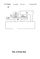
- FIG. 1 is a top view of a chemical mechanical polishing (CMP) machine 100 and FIG. 2 is a side view of CMP machine 100 .
- CMP machine 100 is fed semiconductor wafers to be polished.
- CMP machine 100 picks up the wafers with an arm 101 and places them onto a rotating polishing pad 102 .
- Polishing pad 102 is made of a resilient material and is textured, often with a plurality of predetermined grooves 103 , to aid the polishing process.
- Polishing pad 102 rotates on a platen 104 , or turn table located beneath polishing pad 102 , at a predetermined speed.
- a wafer 105 is held in place on polishing pad 102 within a carrier ring 112 that is connected to a carrier film 106 of arm 101 .
- CMP machine 100 also includes a slurry dispense arm 107 extending across the radius of polishing pad 102 , which dispenses a flow of slurry onto polishing pad 102 .
- the slurry is a mixture of deionized water and polishing agents designed to chemically aid the smooth and predictable planarization of wafer 105 .
- the rotating action of both polishing pad 102 and wafer 105 in conjunction with the polishing action of the slurry, combine to planarize, or polish, wafer 105 at some nominal rate. This rate is referred to as the removal rate.
- a constant and predictable removal rate is important to the uniformity and throughput performance of the wafer fabrication process.
- the removal rate should be expedient, yet yield precisely planarized wafers, free from surface anomalies. If the removal rate is too slow, the number of planarized wafers produced in a given period of time decreases, hurting wafer throughput of the fabrication process. If the removal rate is too fast, the CMP planarization process will not be consistent across several wafers in a batch, thereby hurting the consistency of the fabrication process.
- CMP machine 100 includes a conditioner assembly 120 .
- Conditioner assembly 120 includes a conditioner arm 108 , which extends across the radius of polishing pad 102 .
- An end effector 109 is connected to conditioner arm 108 .
- End effector 109 includes an abrasive conditioning disk 110 which is used to roughen the surface of polishing pad 102 .
- Conditioning disk 110 is rotated by conditioner arm 108 and is translationally moved towards the center of the polishing pad 102 and away from the center of polishing pad 102 , such that conditioning disk 110 covers the radius of polishing pad 102 . In so doing, conditioning disk 110 covers the surface area of polishing pad 102 , as polishing pad 102 rotates.
- a polishing pad having a roughened surface has an increased number of micro-pits and gouges in its surface from conditioner assembly 120 and therefore produces a faster removal rate via increased slurry transfer to the surface of wafer 105 . Without conditioning, the surface of polishing pad 102 is smoothed during the polishing process and removal rate decreases dramatically. Conditioner assembly 120 re-roughens the surface of polishing pad 102 , thereby improving the transport of slurry and improving the removal rate.
- the CMP process uses an abrasive slurry on a polishing pad.
- the polishing action of the slurry is comprised of an abrasive frictional component and a chemical component.
- the abrasive frictional component is due to the friction between the surface of the polishing pad, the surface of the wafer, and abrasive particles suspended in the slurry.
- the chemical component is due to the presence in the slurry of polishing agents which chemically interact with the material of the dielectric layer of wafer 105 .
- the chemical component of the slurry is used to soften the surface of the dielectric layer to be polished, while the frictional component removes material from the surface of wafer 105 .
- the polishing action of the slurry determines the removal rate and removal rate uniformity, and thus, the effectiveness of the CMP process.
- the transport of fresh slurry to the surface of wafer 105 and the removal of polishing by-products away from the surface of wafer 105 becomes very important in maintaining the removal rate.
- Slurry transport is facilitated by the texture of the surface of polishing pad 102 .
- This texture is comprised of both predefined grooves 103 and micro-pits that are manufactured into the surface of polishing pad 102 and the inherently rough surface of the material from which polishing pad 102 is made.
- the slurry is transported by grooves 103 and micro-pits of polishing pad 102 under the edges of wafer 105 as both polishing pad 102 and wafer 105 rotate. Consumed slurry and polishing by-products, in a similar manner, are also transported by grooves 103 and micro-pits of polishing pad 102 away from the surface of wafer 105 . As the polishing process continues, fresh slurry is continually dispensed onto polishing pad 102 from slurry dispense arm 107 . The polishing process continues until wafer 105 is sufficiently planarized and removed from polishing pad 102 .
- endpoint detection is a way of determining when to stop the CMP process of a semiconductor wafer.
- endpoint detection technique involves using reflected incident light to determine the thickness of a film (e.g., oxide) on wafer 105 during the CMP process. Once the film achieves a desired thickness, the CMP process is discontinued.
- this prior art endpoint detection technique typically includes a transparent window slit 114 of FIG. 1 that is located within polishing pad 102 and enables incident light to pass through it. Furthermore, window slit 114 is positioned within polishing pad 102 such that wafer 105 passes over it every time polishing pad 102 makes a complete rotation. In other words, every time polishing pad 102 rotates during the CMP process, window slit 114 passes underneath wafer 105 . As wafer 105 passes over window slit 114 , incident light shines through window slit 114 and reflects off of different surfaces within wafer 105 .
- a single wavelength or different wavelengths of reflected incident light are then used to determine the thickness of a film on wafer 105 during the CMP process.
- the CMP process of wafer 105 is discontinued.
- FIG. 3 shows incident light rays 302 - 308 reflecting off of different surfaces within a side sectional view of semiconductor wafer 105 . Since incident light rays 302 - 308 each reflect off of different surfaces at different depths within wafer 105 , a subsequent film thickness determination of any particular layer using reflected incident light rays 302 - 308 is difficult. This is referred to as pattern density effects. As such, determining when the desired endpoint has been reached during the CMP process of wafer 105 becomes more difficult and therefore results in less control of the film removal process.
- Another factor that causes the prior art light reflection endpoint detection technique to provide inaccurate endpoint detection during a CMP process of semiconductor wafers is that it is difficult to precisely align window slit 114 of FIG. 1 with a particular desirable region of semiconductor wafer 105 .
- polishing pad 102 is rotating at the same time arm 101 rotates wafer 105 at a predetermined rate.
- the reflected incident light rays 302 - 308 of FIG. 3 also represent what would be typically received from wafer 105 during a film thickness determination of any particular layer.
- the received reflected incident light rays 302 - 308 make it difficult to determine the film thickness of any particular layer thereby reducing the accuracy at which the desired endpoint can be detected. Therefore, the prior art endpoint detection technique described above is undesirable because it does not provide accurate endpoint detection during a CMP process of semiconductor wafers.
- the present invention provides a method and system that provides more accurate endpoint detection during a chemical mechanical polishing (CMP) process of semiconductor wafers.
- CMP chemical mechanical polishing
- an operator of a CMP machine knows precisely when to stop a CMP process of a semiconductor wafer.
- the present invention enables the operator of the CMP machine to know within a certain accuracy the film (e.g., dielectric layer) thickness remaining after the CMP process of the semiconductor wafer.
- the present invention essentially eliminates excessive chemical mechanical polishing of the semiconductor wafer. As such, not as much dielectric material needs to be deposited on the wafer in order to compensate for excessive chemical mechanical polishing of the semiconductor wafer. Therefore, the present invention is able to reduce fabrication costs of semiconductor wafers.
- one embodiment of the present invention includes a method for improving chemical mechanical polishing endpoint detection.
- the method comprises the step of depositing a dielectric layer over a reflectance stop layer.
- the reflectance stop layer is disposed above a component that is disposed on a semiconductor wafer.
- the reflectance stop layer substantially reduces any light from reflecting off of the component.
- Another embodiment of the present invention also includes a method for improving chemical mechanical polishing endpoint detection.
- the method comprises the step of depositing a reflectance stop layer above a component that is disposed on a semiconductor wafer.
- the reflectance stop layer substantially reduces any light from reflecting off of the component.
- the method also includes the step of depositing a dielectric layer over the reflectance stop layer and the component.
- Another step of the method includes removing material from the dielectric layer disposed above the semiconductor wafer using a chemical mechanical polishing process.
- the method further includes the step of determining the thickness of the dielectric layer disposed above the semiconductor wafer using a reflected signal of light. In response to the dielectric layer substantially achieving a desired thickness, the method includes the step of stopping the chemical mechanical polishing process of the semiconductor wafer.
- the present invention comprises the step of depositing a first dielectric layer above a reflectance stop layer.
- the reflectance stop layer is disposed above a second dielectric layer.
- the second dielectric layer is disposed over a component that is disposed on a semiconductor wafer. During a determination of the thickness of said second dielectric layer above said component using a reflected signal of light, the reflectance stop layer substantially reduces any light from reflecting off of other surfaces except said component.
- Another embodiment of the present invention comprises the step of depositing a first dielectric layer over a component disposed on a semiconductor wafer.
- the method includes the step of depositing a reflectance stop layer above the first dielectric layer.
- the method includes the step of depositing a second dielectric layer above the reflectance stop layer.
- Another step of the method includes removing material from the second dielectric layer and the reflectance stop layer disposed above the semiconductor wafer using a chemical mechanical polishing process.
- the second dielectric layer and the reflectance stop layer subsequently are substantially removed from above the component.
- the method further includes the step of determining the thickness of the first dielectric layer above the component using a reflected signal of light.
- the reflectance stop layer that remains substantially reduces any light from reflecting off of other surfaces except the component.
- the method includes the step of stopping the chemical mechanical polishing process of the semiconductor wafer.
- FIG. 1 is a top view of a prior art chemical mechanical polishing machine.
- FIG. 2 is a side view of the prior art chemical mechanical polishing machine of FIG. 1 .
- FIG. 3 shows incident light reflecting off of a side sectional view of a semiconductor wafer in order to determine the thickness of its films during a chemical mechanical polishing process.
- FIG. 4A is a top view of a chemical mechanical polishing machine in accordance with one embodiment of the present invention.
- FIG. 4B is a side view of the chemical mechanical polishing machine of FIG. 4 A.
- FIG. 5A is a side sectional view of a semiconductor wafer having a reflectance stop layer deposited above metal components in accordance with one embodiment of the present invention.
- FIG. 5B shows incident light reflecting off of the semiconductor wafer of FIG. 5A in order to determine the thickness of its films during a chemical mechanical polishing process.
- FIG. 6A is a side sectional view of a semiconductor wafer having a reflectance stop layer deposited between two dielectric layers in accordance with one embodiment of the present invention.
- FIG. 6B shows incident light reflecting off of the semiconductor wafer of FIG. 6A in order to determine the thickness of its films during a chemical mechanical polishing process.
- FIG. 7 is a flowchart of a method in accordance with one embodiment of the present invention for improving chemical mechanical polishing endpoint detection during planarization of semiconductor wafers.
- FIG. 8 is a flowchart of a method in accordance with another embodiment of the present invention for improving chemical mechanical polishing endpoint detection during planarization of semiconductor wafers.
- CMP Chemical mechanical polishing
- the CMP process involves removing all, or a portion of, a layer of dielectric material using mechanical contact between the wafer and a moving polishing pad saturated with a polishing slurry. Polishing through the CMP process flattens out height differences, since high areas of topography (hills) are removed faster than areas of low topography (valleys).
- the CMP process has the capability of smoothing out topography over millimeter scale planarization distances, leading to maximum angles of much less than one degree after polishing.
- complex ICs often have many different built up layers, each layer having components, each layer having differing interconnections, and each layer fabricated on top of the previous layer.
- One of the techniques for fabricating the individual layers of complex ICs is to encase the metal components of each layer within dielectric material, commonly referred to as an inter-metal dielectric layer.
- the purpose of the inter-metal dielectric layer is to electrically isolate the metal components of one layer from the metal components of previous and/or subsequent layers. Once an inter-metal dielectric layer is fabricated, another layer of components is subsequently fabricated on top of it.
- the present invention provides a method and system that provides more accurate endpoint detection during a chemical mechanical polishing process of semiconductor wafers.
- One embodiment of the present invention includes the implementation of the endpoint detection technique of using reflected incident light to determine the thickness of a film (e.g., oxide) on a semiconductor wafer during a CMP process, as described above.
- a film e.g., oxide
- the present invention enables the operator of the CMP machine to know within a certain accuracy the film (e.g., dielectric layer) thickness remaining after the CMP process of the semiconductor wafer. Moreover, the present invention essentially eliminates excessive chemical mechanical polishing of the semiconductor wafer. As such, not as much dielectric material needs to be deposited on the wafer in order to compensate for excessive chemical mechanical polishing of the semiconductor wafer. Therefore, the present invention is able to reduce fabrication costs of semiconductor wafers.
- the CMP endpoint detection method of the present invention and its benefits are described in greater detail below.
- FIG. 4A shows a top view of a chemical mechanical polishing (CMP) machine 400 in accordance with one embodiment of the present invention utilized for chemical mechanical polishing of semiconductor wafers.
- FIG. 4B shows a side view of CMP machine 400 .
- CMP machine 400 picks up a semiconductor wafer 410 , which was fabricated in accordance with an embodiment of the present invention, with an arm 402 and places it onto the rotating polishing pad 404 .
- Polishing pad 404 is made of a resilient material and is textured typically with a plurality of grooves 406 to aid the polishing process. Polishing pad 404 of CMP machine 400 rotates at a predetermined speed on a platen 408 , or turn table located beneath polishing pad 404 .
- Arm 402 forces wafer 410 into polishing pad 404 with a predetermined amount of down force.
- Wafer 410 is held in place on the polishing pad 404 by a carrier ring 412 and a carrier film 414 of arm 402 .
- the front surface of wafer 410 rests against the polishing pad 404 while the back surface of wafer 410 is against the lower surface of carrier film 414 of arm 402 .
- arm 402 also rotates wafer 410 at a predetermined rate.
- CMP machine 400 also includes a slurry dispense arm 416 extending across the radius of polishing pad 404 .
- Slurry dispense arm 416 dispenses a flow of slurry onto polishing pad 404 .
- CMP machine 400 further includes a conditioner assembly 418 which consists of an end effector 420 and a conditioner arm 422 that extends across the radius of polishing pad 404 .
- End effector 420 is connected to conditioner arm 422 and includes an abrasive disk 424 that is used to roughen the surface of the polishing pad 404 , in the manner described above.
- the dispensed slurry is transported by grooves 406 and micro-pits of polishing pad 404 under the edges of wafer 410 as both polishing pad 404 and wafer 404 rotate. Consumed slurry and polishing by-products, in a similar manner, are also transported by grooves 406 and micro-pits of polishing pad 404 away from the surface of wafer 410 . As the polishing process continues, fresh slurry is continually dispensed onto polishing pad 404 from slurry dispense arm 416 . The polishing process of wafer 410 continues until its desired endpoint is detected. Once the endpoint is detected, the CMP process of wafer 410 is discontinued.
- the endpoint detection technique implemented within the present embodiment involves using reflected incident light to determine the thickness of a film (e.g., dielectric) on wafer 410 during the CMP process. Once the film achieves a desired thickness, the CMP process is suspended.
- This endpoint detection technique is well known by those of ordinary skill in the art.
- the endpoint detection technique implemented within the present embodiment includes a transparent window slit 426 of FIG. 4A that is located within polishing pad 404 and enables incident light to pass through it.
- window slit 426 is positioned within polishing pad 404 such that wafer 410 passes over it every time polishing pad 404 makes a complete rotation.
- window slit 426 passes underneath wafer 410 .
- incident light shines through window slit 426 and reflects off of different surfaces within wafer 410 .
- a single wavelength or different wavelengths of reflected incident light are then used to determine the thickness of the film on wafer 410 during the CMP process. Once the film achieves a desired thickness, the CMP process of wafer 410 is ended.
- FIG. 5A is a side sectional view of semiconductor wafer 410 having reflectance stop layers 508 and 510 located above components 504 and 506 , respectively, in accordance with one embodiment of the present invention.
- a dielectric layer 512 is deposited over reflectance stop layers 508 and 510 , components 504 and 506 , and substrate 502 of semiconductor wafer 410 .
- dielectric layer 512 in accordance with the present embodiment, include any type of non-conductive material (e.g., oxide, polymer, and the like).
- embodiments of reflectance stop layers 508 and 510 include silicon oxy-nitride, amorphous silicon, and the like.
- embodiments of components 504 and 506 in accordance with the present embodiment, include any type of conductive material (e.g., aluminum, copper, silver, gold, and the like).
- FIG. 5B shows a determination of the thickness of dielectric layer 512 using incident light (e.g., incident light rays 514 - 518 ) during a CMP process of semiconductor wafer 410 .
- incident light e.g., incident light rays 514 - 518
- the main purpose of reflectance stop layers 508 and 510 within the present embodiment, is to suppress incident light from reflecting off of underlying components 504 and 508 . As such, reflected incident light is substantially obtained from substrate 502 .
- any changes in the reflectance of incident light during the CMP process is merely attributed to a change in the thickness of dielectric layer 512 . Therefore, by providing a more accurate measurement of the thickness of dielectric layer 512 , the present embodiment provides more accurate endpoint detection during the CMP process.
- transparent window slit 426 passes underneath wafer 410 .
- incident light rays 514 - 518 pass through window slit 426 and shine on wafer 410 as shown in FIG. 5 B.
- incident light rays 514 and 516 pass through dielectric layer 512 and are subsequently absorbed by reflectance stop layers 504 and 508 , respectively.
- incident light ray 518 passes through dielectric layer 512 , reflects off of substrate 502 , and subsequently passes through dielectric layer 512 to eventually be used to determine the thickness of dielectric layer 512 . Therefore, the present embodiment limits what incident light rays 514 - 518 reflect off of within wafer 410 .
- reflectance stop layers 508 and 510 are deposited too thin above components 504 and 506 , they will not sufficiently suppress the reflection of incident light in the course of a determination of the thickness of dielectric layer 512 during a CMP process. As such, it is important that a proper thickness of reflectance stop layers 508 and 510 are deposited above components 504 and 506 , within the present embodiment. As such, the following examples illustrates this point. Given the wavelength of incident light to be used to determine the thickness of dielectric layer 512 is 450 nanometers (nm). Furthermore, reflectance stop layers 508 and 510 are an amorphous silicon having an absorption coefficient of about 4 ⁇ 10 5 /cm.
- reflectance stop layers 508 and 510 each provide 87% absorption of that particular wavelength of incident light. Moreover, if 1000 angstroms of reflectance stop layers 508 and 510 are deposited above components 504 and 506 , reflectance stop layers 508 and 510 each provide 98% absorption of that particular wavelength of incident light. Within the present embodiment, it should be appreciated that reflectance stop layers 508 and 510 are not limited to these specific examples of thickness.
- semiconductor wafer 600 includes a component 612 which is disposed on a substrate 614 .
- a dielectric layer 616 is deposited over component 612 and substrate 614 .
- components 608 and 610 are disposed on dielectric layer 616 of semiconductor wafer 600 .
- a dielectric layer 606 is deposited over dielectric layer 616 and components 608 and 610 .
- semiconductor includes a reflectance stop layer 602 which is deposited above dielectric layer 606 .
- a dielectric layer 604 is deposited above reflectance stop layer 602 of wafer 600 .
- dielectric layers 604 , 606 , and 616 include any type of non-conductive material (e.g., oxide, polymer, and the like).
- embodiments of reflectance stop layer 602 include silicon oxy-nitride, amorphous silicon, and the like.
- embodiments of components 608 - 612 include any type of conductive material (e.g., aluminum, copper, silver, gold, and the like).
- FIG. 6B shows a determination of the thickness of dielectric layer 606 above components 608 and 610 using incident light (e.g., incident light rays 618 - 622 ) during a CMP process of semiconductor wafer 600 .
- incident light e.g., incident light rays 618 - 622
- reflectance stop layer 602 has been preferentially removed from above components 608 and 610 during the CMP process since high areas of topography (hills) are removed faster than areas of low topography (valleys).
- the remaining portions of reflectance stop layer 602 within the present embodiment act as absorption layers that block incident light reflection from underlying component 612 and substrate 614 .
- reflected incident light is substantially obtained from components 608 and 610 .
- any changes in the reflectance of incident light during the CMP process is merely attributed to a change in the thickness of dielectric layer 606 above components 608 and 610 . Therefore, by providing a more accurate measurement of the thickness of dielectric layer 606 above components 608 and 610 , the present embodiment provides more accurate endpoint detection during the CMP process. It should be appreciated that endpoint detection of the present embodiment is set to start determining the thickness of dielectric layer 606 once reflectance stop layer 602 has been polished away from above components 608 and 610 as shown in FIG. 6 B.
- transparent window slit 426 passes underneath wafer 600 .
- incident light rays 618 - 622 pass through window slit 426 and shine on wafer 600 as shown in FIG. 6 B.
- incident light ray 618 passes through dielectric layer 604 and is subsequently absorbed by reflectance stop layer 602 .
- incident light rays 620 and 622 pass through dielectric layer 606 , reflect off of components 608 and 610 , respectively, and subsequently pass through dielectric layer 606 .
- reflected incident light rays 620 and 622 are used to determine the thickness of dielectric layer 606 above components 608 and 610 . Therefore, the present embodiment limits what incident light rays 618 - 622 reflect off of within wafer 600 .
- steps 702 in one embodiment of the present invention, components 504 and 506 of FIGS. 5A and 5B are patterned on substrate 502 of semiconductor wafer 410 .
- components 504 and 506 can be patterned on surfaces other than substrate 502 (e.g., dielectric layer).
- reflectance stop layers 508 and 510 are deposited and patterned above components 504 and 506 , respectively, of semiconductor wafer 410 .
- dielectric layer 512 is deposited over reflectance stop layers 508 and 510 , components 504 and 506 , and substrate 502 of semiconductor wafer 410 .
- CMP machine 400 of FIGS. 4A and 4B removes material from dielectric layer 512 by performing a chemical mechanical polishing process on semiconductor wafer 410 , as described above.
- the present embodiment determines the thickness of dielectric layer 512 of semiconductor wafer 410 using incident light during the CMP process, as described above.
- the present embodiment determines whether dielectric layer 512 of semiconductor wafer 410 has substantially achieved a desired thickness. If dielectric layer 512 of semiconductor wafer 410 has not substantially achieved the desired thickness, the present embodiment proceeds to step 708 . If dielectric layer 512 of semiconductor wafer 410 has substantially achieved the desired thickness, the present embodiment proceeds to step 714 .
- step 714 CMP machine 400 of the present embodiment stops performing the chemical mechanical polishing process on dielectric layer 512 of semiconductor wafer 410 , as described above.
- steps 802 in one embodiment of the present invention, components 608 and 610 of FIGS. 6A and 6B are patterned on dielectric layer 616 of semiconductor wafer 600 .
- components 608 and 610 can be patterned on surfaces other than dielectric layer 616 (e.g., substrate 614 ).
- dielectric layer 606 is deposited over dielectric layer 616 and components 608 and 610 of semiconductor wafer 600 of the present embodiment.
- reflectance stop layer 602 is deposited above dielectric layer 606 of semiconductor wafer 600 .
- dielectric layer 604 is deposited over reflectance stop layer 602 of semiconductor wafer 600 .
- CMP machine 400 of FIGS. 4A and 4B removes material from dielectric layer 604 , reflectance stop layer 602 , and dielectric layer 606 by performing a chemical mechanical polishing process on semiconductor wafer 600 , as described above.
- the present embodiment determines the thickness of dielectric layer 606 above components 608 and 610 of semiconductor wafer 600 by using incident light during the CMP process, as described above. It should be appreciated that endpoint detection of the present embodiment is set to start determining the thickness of dielectric layer 606 once reflectance stop layer 602 has been polished away from above components 608 and 610 as shown in FIG. 6 B.
- the present embodiment determines whether dielectric layer 606 of semiconductor wafer 600 has substantially achieved a desired thickness above components 608 and 610 . If dielectric layer 606 of semiconductor wafer 600 has not substantially achieved the desired thickness above components 608 and 610 , the present embodiment proceeds to step 810 . If dielectric layer 606 of semiconductor wafer 600 has substantially achieved the desired thickness above components 608 and 610 , the present embodiment proceeds to step 816 .
- step 816 CMP machine 400 of the present embodiment stops performing the chemical mechanical polishing process on semiconductor wafer 600 , as described above.
- the present invention provides a method and system that provides more accurate endpoint detection during a CMP process of semiconductor wafers.
- an operator of a CMP machine knows precisely when to stop a CMP process of a semiconductor wafer.
- the present invention enables the operator of the CMP machine to know within a certain accuracy the film (e.g., dielectric layer) thickness remaining after the CMP process of the semiconductor wafer.
- the present invention essentially eliminates excessive chemical mechanical polishing of the semiconductor wafer. As such, not as much dielectric material needs to be deposited on the wafer in order to compensate for excessive chemical mechanical polishing of the semiconductor wafer. Therefore, the present invention is able to reduce fabrication costs of semiconductor wafers.
Abstract
Description
Claims (26)
Priority Applications (2)
| Application Number | Priority Date | Filing Date | Title |
|---|---|---|---|
| US09/197,377 US6214734B1 (en) | 1998-11-20 | 1998-11-20 | Method of using films having optimized optical properties for chemical mechanical polishing endpoint detection |
| US09/523,403 US6649253B1 (en) | 1998-11-20 | 2000-03-10 | Method of using films having optimized optical properties for chemical mechanical polishing endpoint detection |
Applications Claiming Priority (1)
| Application Number | Priority Date | Filing Date | Title |
|---|---|---|---|
| US09/197,377 US6214734B1 (en) | 1998-11-20 | 1998-11-20 | Method of using films having optimized optical properties for chemical mechanical polishing endpoint detection |
Related Child Applications (1)
| Application Number | Title | Priority Date | Filing Date |
|---|---|---|---|
| US09/523,403 Division US6649253B1 (en) | 1998-11-20 | 2000-03-10 | Method of using films having optimized optical properties for chemical mechanical polishing endpoint detection |
Publications (1)
| Publication Number | Publication Date |
|---|---|
| US6214734B1 true US6214734B1 (en) | 2001-04-10 |
Family
ID=22729154
Family Applications (2)
| Application Number | Title | Priority Date | Filing Date |
|---|---|---|---|
| US09/197,377 Expired - Lifetime US6214734B1 (en) | 1998-11-20 | 1998-11-20 | Method of using films having optimized optical properties for chemical mechanical polishing endpoint detection |
| US09/523,403 Expired - Fee Related US6649253B1 (en) | 1998-11-20 | 2000-03-10 | Method of using films having optimized optical properties for chemical mechanical polishing endpoint detection |
Family Applications After (1)
| Application Number | Title | Priority Date | Filing Date |
|---|---|---|---|
| US09/523,403 Expired - Fee Related US6649253B1 (en) | 1998-11-20 | 2000-03-10 | Method of using films having optimized optical properties for chemical mechanical polishing endpoint detection |
Country Status (1)
| Country | Link |
|---|---|
| US (2) | US6214734B1 (en) |
Cited By (37)
| Publication number | Priority date | Publication date | Assignee | Title |
|---|---|---|---|---|
| US6395563B1 (en) * | 1998-12-28 | 2002-05-28 | Matsushita Electric Industrial Co., Ltd. | Device for manufacturing semiconductor device and method of manufacturing the same |
| US20020103866A1 (en) * | 2000-11-30 | 2002-08-01 | Chi Yueh-Shian T. | Dynamic subject information generation in message services of distributed object systems |
| US20020128735A1 (en) * | 2001-03-08 | 2002-09-12 | Hawkins Parris C.M. | Dynamic and extensible task guide |
| US20020138321A1 (en) * | 2001-03-20 | 2002-09-26 | Applied Materials, Inc. | Fault tolerant and automated computer software workflow |
| US20020156548A1 (en) * | 1999-07-29 | 2002-10-24 | Applied Materials, Inc. | Computer integrated manufacturing techniques |
| US6475879B2 (en) * | 2000-01-18 | 2002-11-05 | Seiko Epson Corporation | Semiconductor wafer, method for processing the same and method for manufacturing semiconductor device |
| US20020197745A1 (en) * | 2001-06-19 | 2002-12-26 | Shanmugasundram Arulkumar P. | Feedback control of a chemical mechanical polishing device providing manipulation of removal rate profiles |
| US20030027424A1 (en) * | 2001-06-19 | 2003-02-06 | Paik Young Joseph | Feedforward and feedback control for conditioning of chemical mechanical polishing pad |
| US20030049390A1 (en) * | 2001-06-19 | 2003-03-13 | Applied Materials, Inc. | Feedback control of plasma-enhanced chemical vapor deposition processes |
| US20030049376A1 (en) * | 2001-06-19 | 2003-03-13 | Applied Materials, Inc. | Feedback control of sub-atmospheric chemical vapor deposition processes |
| US20030180972A1 (en) * | 2002-03-19 | 2003-09-25 | Amir Al-Bayati | Method, system and medium for controlling semiconductor wafer processes using critical dimension measurements |
| US20030194945A1 (en) * | 2002-04-10 | 2003-10-16 | Drown Jennifer Lynne | Method and apparatus for detection of chemical mechanical planarization endpoint and device planarity |
| US20030199112A1 (en) * | 2002-03-22 | 2003-10-23 | Applied Materials, Inc. | Copper wiring module control |
| US6640151B1 (en) | 1999-12-22 | 2003-10-28 | Applied Materials, Inc. | Multi-tool control system, method and medium |
| US20030202070A1 (en) * | 2002-04-29 | 2003-10-30 | Xerox Corporation | Multiple portion solid ink stick |
| US6649253B1 (en) * | 1998-11-20 | 2003-11-18 | Koninklijke Philips Electronics N.V. | Method of using films having optimized optical properties for chemical mechanical polishing endpoint detection |
| US20040038502A1 (en) * | 2002-06-26 | 2004-02-26 | Sethuraman Jayashankar | Method of detecting chemical mechanical polishing endpoints in thin film head processes |
| US20040038534A1 (en) * | 2002-08-21 | 2004-02-26 | Taylor Theodore M. | Apparatus and method for conditioning a polishing pad used for mechanical and/or chemical-mechanical planarization |
| US6708074B1 (en) | 2000-08-11 | 2004-03-16 | Applied Materials, Inc. | Generic interface builder |
| US20040063224A1 (en) * | 2002-09-18 | 2004-04-01 | Applied Materials, Inc. | Feedback control of a chemical mechanical polishing process for multi-layered films |
| US20040080050A1 (en) * | 2002-10-24 | 2004-04-29 | Lam Research Corporation | Method and apparats for detecting endpoint during plasma etching of thin films |
| US20040080368A1 (en) * | 2002-10-29 | 2004-04-29 | Pravas Pradhan | Low voltage, low power differential receiver |
| US20040148049A1 (en) * | 2003-01-21 | 2004-07-29 | Applied Materials, Inc. | Automated design and execution of experiments with integrated model creation for semiconductor manufacturing tools |
| US6809032B1 (en) * | 2002-05-01 | 2004-10-26 | Advanced Micro Devices, Inc. | Method and apparatus for detecting the endpoint of a chemical-mechanical polishing operation using optical techniques |
| US20040248409A1 (en) * | 2003-06-03 | 2004-12-09 | Applied Materials, Inc. | Selective metal encapsulation schemes |
| US20050014299A1 (en) * | 2003-07-15 | 2005-01-20 | Applied Materials, Inc. | Control of metal resistance in semiconductor products via integrated metrology |
| US20050032459A1 (en) * | 2003-08-04 | 2005-02-10 | Applied Materials, Inc. | Technique for process-qualifying a semiconductor manufacturing tool using metrology data |
| US20050171626A1 (en) * | 2004-01-29 | 2005-08-04 | Applied Materials, Inc. | System, method, and medium for monitoring performance of an advanced process control system |
| US20050267607A1 (en) * | 2004-05-28 | 2005-12-01 | Applied Materials, Inc. | Dynamic offset and feedback threshold |
| US20050278051A1 (en) * | 2004-05-28 | 2005-12-15 | Applied Materials, Inc. | Process control by distinguishing a white noise component of a process variance |
| US20060025054A1 (en) * | 2004-08-02 | 2006-02-02 | Mayes Brett A | Systems and methods for actuating end effectors to condition polishing pads used for polishing microfeature workpieces |
| US20060079007A1 (en) * | 2004-10-08 | 2006-04-13 | Applied Materials, Inc. | System, method, and medium for an endpoint detection scheme for copper low-dielectric damascene structures for improved dielectric and copper loss |
| US20070055267A1 (en) * | 1997-06-09 | 2007-03-08 | Kyphon Inc. | Methods and devices for treating fractured and/or diseased bone using a mesh structure |
| US20080021571A1 (en) * | 2002-11-15 | 2008-01-24 | Yuri Kokotov | Method, system and medium for controlling manufacture process having multivariate input parameters |
| US20080109089A1 (en) * | 2001-06-19 | 2008-05-08 | Shanmugasundram Arulkumar P | Dynamic metrology schemes and sampling schemes for advanced process control in semiconductor processing |
| US20090093071A1 (en) * | 2007-10-09 | 2009-04-09 | Fujitsu Microelectronics Limited | Thermal treatment apparatus, thermal treatment method and method of manufacturing semiconductor device |
| US8404129B1 (en) * | 2010-03-31 | 2013-03-26 | Western Digital (Fremont), Llc | Method and system for providing a curved surface in a magnetic recording head |
Citations (5)
| Publication number | Priority date | Publication date | Assignee | Title |
|---|---|---|---|---|
| US5731239A (en) * | 1997-01-22 | 1998-03-24 | Chartered Semiconductor Manufacturing Pte Ltd. | Method of making self-aligned silicide narrow gate electrodes for field effect transistors having low sheet resistance |
| US5795495A (en) * | 1994-04-25 | 1998-08-18 | Micron Technology, Inc. | Method of chemical mechanical polishing for dielectric layers |
| US5835226A (en) * | 1997-11-13 | 1998-11-10 | Lsi Logic Corporation | Method for determining optical constants prior to film processing to be used improve accuracy of post-processing thickness measurements |
| US5910022A (en) * | 1997-05-22 | 1999-06-08 | Vlsi Technology, Inc. | Method and system for tungsten chemical mechanical polishing for unplanarized dielectric surfaces |
| US6013574A (en) * | 1996-01-30 | 2000-01-11 | Advanced Micro Devices, Inc. | Method of forming low resistance contact structures in vias arranged between two levels of interconnect lines |
Family Cites Families (5)
| Publication number | Priority date | Publication date | Assignee | Title |
|---|---|---|---|---|
| US5792707A (en) * | 1997-01-27 | 1998-08-11 | Chartered Semiconductor Manufacturing Ltd. | Global planarization method for inter level dielectric layers of integrated circuits |
| US6117777A (en) * | 1997-07-30 | 2000-09-12 | Chartered Semiconductor Manufacturing Co. | Chemical mechanical polish (CMP) endpoint detection by colorimetry |
| US6080670A (en) * | 1998-08-10 | 2000-06-27 | Lsi Logic Corporation | Method of detecting a polishing endpoint layer of a semiconductor wafer which includes a non-reactive reporting specie |
| US6191037B1 (en) * | 1998-09-03 | 2001-02-20 | Micron Technology, Inc. | Methods, apparatuses and substrate assembly structures for fabricating microelectronic components using mechanical and chemical-mechanical planarization processes |
| US6214734B1 (en) * | 1998-11-20 | 2001-04-10 | Vlsi Technology, Inc. | Method of using films having optimized optical properties for chemical mechanical polishing endpoint detection |
-
1998
- 1998-11-20 US US09/197,377 patent/US6214734B1/en not_active Expired - Lifetime
-
2000
- 2000-03-10 US US09/523,403 patent/US6649253B1/en not_active Expired - Fee Related
Patent Citations (5)
| Publication number | Priority date | Publication date | Assignee | Title |
|---|---|---|---|---|
| US5795495A (en) * | 1994-04-25 | 1998-08-18 | Micron Technology, Inc. | Method of chemical mechanical polishing for dielectric layers |
| US6013574A (en) * | 1996-01-30 | 2000-01-11 | Advanced Micro Devices, Inc. | Method of forming low resistance contact structures in vias arranged between two levels of interconnect lines |
| US5731239A (en) * | 1997-01-22 | 1998-03-24 | Chartered Semiconductor Manufacturing Pte Ltd. | Method of making self-aligned silicide narrow gate electrodes for field effect transistors having low sheet resistance |
| US5910022A (en) * | 1997-05-22 | 1999-06-08 | Vlsi Technology, Inc. | Method and system for tungsten chemical mechanical polishing for unplanarized dielectric surfaces |
| US5835226A (en) * | 1997-11-13 | 1998-11-10 | Lsi Logic Corporation | Method for determining optical constants prior to film processing to be used improve accuracy of post-processing thickness measurements |
Cited By (63)
| Publication number | Priority date | Publication date | Assignee | Title |
|---|---|---|---|---|
| US20070055267A1 (en) * | 1997-06-09 | 2007-03-08 | Kyphon Inc. | Methods and devices for treating fractured and/or diseased bone using a mesh structure |
| US6695947B2 (en) | 1998-05-07 | 2004-02-24 | Matsushita Electric Industrial Co., Ltd. | Device for manufacturing semiconductor device and method of manufacturing the same |
| US6649253B1 (en) * | 1998-11-20 | 2003-11-18 | Koninklijke Philips Electronics N.V. | Method of using films having optimized optical properties for chemical mechanical polishing endpoint detection |
| US20020135785A1 (en) * | 1998-12-28 | 2002-09-26 | Matsushita Electric Industrial Co., Ltd. | Device for manufacturing semiconductor device and method of manufacturing the same |
| US6750976B2 (en) | 1998-12-28 | 2004-06-15 | Matsushita Electric Industrial Co., Ltd. | Device for manufacturing semiconductor device and method of manufacturing the same |
| US6395563B1 (en) * | 1998-12-28 | 2002-05-28 | Matsushita Electric Industrial Co., Ltd. | Device for manufacturing semiconductor device and method of manufacturing the same |
| US20020156548A1 (en) * | 1999-07-29 | 2002-10-24 | Applied Materials, Inc. | Computer integrated manufacturing techniques |
| US20040083021A1 (en) * | 1999-12-22 | 2004-04-29 | Applied Materials, Inc. | Multi-tool control system, method and medium |
| US6640151B1 (en) | 1999-12-22 | 2003-10-28 | Applied Materials, Inc. | Multi-tool control system, method and medium |
| US6475879B2 (en) * | 2000-01-18 | 2002-11-05 | Seiko Epson Corporation | Semiconductor wafer, method for processing the same and method for manufacturing semiconductor device |
| US6708074B1 (en) | 2000-08-11 | 2004-03-16 | Applied Materials, Inc. | Generic interface builder |
| US20070112928A1 (en) * | 2000-11-30 | 2007-05-17 | Applied Materials, Inc. | Dynamic subject information generation in message services of distributed object systems |
| US8504620B2 (en) | 2000-11-30 | 2013-08-06 | Applied Materials, Inc. | Dynamic subject information generation in message services of distributed object systems |
| US20020103866A1 (en) * | 2000-11-30 | 2002-08-01 | Chi Yueh-Shian T. | Dynamic subject information generation in message services of distributed object systems |
| US20020128735A1 (en) * | 2001-03-08 | 2002-09-12 | Hawkins Parris C.M. | Dynamic and extensible task guide |
| US20020138321A1 (en) * | 2001-03-20 | 2002-09-26 | Applied Materials, Inc. | Fault tolerant and automated computer software workflow |
| US20020197745A1 (en) * | 2001-06-19 | 2002-12-26 | Shanmugasundram Arulkumar P. | Feedback control of a chemical mechanical polishing device providing manipulation of removal rate profiles |
| US8070909B2 (en) | 2001-06-19 | 2011-12-06 | Applied Materials, Inc. | Feedback control of chemical mechanical polishing device providing manipulation of removal rate profiles |
| US7783375B2 (en) | 2001-06-19 | 2010-08-24 | Applied Materials, Inc. | Dynamic metrology schemes and sampling schemes for advanced process control in semiconductor processing |
| US7725208B2 (en) | 2001-06-19 | 2010-05-25 | Applied Materials, Inc. | Dynamic metrology schemes and sampling schemes for advanced process control in semiconductor processing |
| US8694145B2 (en) | 2001-06-19 | 2014-04-08 | Applied Materials, Inc. | Feedback control of a chemical mechanical polishing device providing manipulation of removal rate profiles |
| US7698012B2 (en) | 2001-06-19 | 2010-04-13 | Applied Materials, Inc. | Dynamic metrology schemes and sampling schemes for advanced process control in semiconductor processing |
| US20080109089A1 (en) * | 2001-06-19 | 2008-05-08 | Shanmugasundram Arulkumar P | Dynamic metrology schemes and sampling schemes for advanced process control in semiconductor processing |
| US20030049376A1 (en) * | 2001-06-19 | 2003-03-13 | Applied Materials, Inc. | Feedback control of sub-atmospheric chemical vapor deposition processes |
| US20030049390A1 (en) * | 2001-06-19 | 2003-03-13 | Applied Materials, Inc. | Feedback control of plasma-enhanced chemical vapor deposition processes |
| US20030027424A1 (en) * | 2001-06-19 | 2003-02-06 | Paik Young Joseph | Feedforward and feedback control for conditioning of chemical mechanical polishing pad |
| US20060009129A1 (en) * | 2001-06-19 | 2006-01-12 | Applied Materials, Inc. | Feedforward and feedback control for conditioning of chemical mechanical polishing pad |
| US20030180972A1 (en) * | 2002-03-19 | 2003-09-25 | Amir Al-Bayati | Method, system and medium for controlling semiconductor wafer processes using critical dimension measurements |
| US20070122921A1 (en) * | 2002-03-22 | 2007-05-31 | Applied Materials, Inc. | Copper Wiring Module Control |
| US8005634B2 (en) | 2002-03-22 | 2011-08-23 | Applied Materials, Inc. | Copper wiring module control |
| US20030199112A1 (en) * | 2002-03-22 | 2003-10-23 | Applied Materials, Inc. | Copper wiring module control |
| US6783426B2 (en) | 2002-04-10 | 2004-08-31 | Agere Systems, Inc. | Method and apparatus for detection of chemical mechanical planarization endpoint and device planarity |
| US20030194945A1 (en) * | 2002-04-10 | 2003-10-16 | Drown Jennifer Lynne | Method and apparatus for detection of chemical mechanical planarization endpoint and device planarity |
| US20030202070A1 (en) * | 2002-04-29 | 2003-10-30 | Xerox Corporation | Multiple portion solid ink stick |
| US6809032B1 (en) * | 2002-05-01 | 2004-10-26 | Advanced Micro Devices, Inc. | Method and apparatus for detecting the endpoint of a chemical-mechanical polishing operation using optical techniques |
| US20040038502A1 (en) * | 2002-06-26 | 2004-02-26 | Sethuraman Jayashankar | Method of detecting chemical mechanical polishing endpoints in thin film head processes |
| US20060199472A1 (en) * | 2002-08-21 | 2006-09-07 | Micron Technology, Inc. | Apparatus and method for conditioning a polishing pad used for mechanical and/or chemical-mechanical planarization |
| US7094695B2 (en) * | 2002-08-21 | 2006-08-22 | Micron Technology, Inc. | Apparatus and method for conditioning a polishing pad used for mechanical and/or chemical-mechanical planarization |
| US20040038534A1 (en) * | 2002-08-21 | 2004-02-26 | Taylor Theodore M. | Apparatus and method for conditioning a polishing pad used for mechanical and/or chemical-mechanical planarization |
| US20040063224A1 (en) * | 2002-09-18 | 2004-04-01 | Applied Materials, Inc. | Feedback control of a chemical mechanical polishing process for multi-layered films |
| US20040080050A1 (en) * | 2002-10-24 | 2004-04-29 | Lam Research Corporation | Method and apparats for detecting endpoint during plasma etching of thin films |
| US6908846B2 (en) * | 2002-10-24 | 2005-06-21 | Lam Research Corporation | Method and apparatus for detecting endpoint during plasma etching of thin films |
| US20040080368A1 (en) * | 2002-10-29 | 2004-04-29 | Pravas Pradhan | Low voltage, low power differential receiver |
| US7966087B2 (en) | 2002-11-15 | 2011-06-21 | Applied Materials, Inc. | Method, system and medium for controlling manufacture process having multivariate input parameters |
| US20080021571A1 (en) * | 2002-11-15 | 2008-01-24 | Yuri Kokotov | Method, system and medium for controlling manufacture process having multivariate input parameters |
| US20040148049A1 (en) * | 2003-01-21 | 2004-07-29 | Applied Materials, Inc. | Automated design and execution of experiments with integrated model creation for semiconductor manufacturing tools |
| US20040248409A1 (en) * | 2003-06-03 | 2004-12-09 | Applied Materials, Inc. | Selective metal encapsulation schemes |
| US20050014299A1 (en) * | 2003-07-15 | 2005-01-20 | Applied Materials, Inc. | Control of metal resistance in semiconductor products via integrated metrology |
| US20050032459A1 (en) * | 2003-08-04 | 2005-02-10 | Applied Materials, Inc. | Technique for process-qualifying a semiconductor manufacturing tool using metrology data |
| US20050171626A1 (en) * | 2004-01-29 | 2005-08-04 | Applied Materials, Inc. | System, method, and medium for monitoring performance of an advanced process control system |
| US20050278051A1 (en) * | 2004-05-28 | 2005-12-15 | Applied Materials, Inc. | Process control by distinguishing a white noise component of a process variance |
| US20060195214A1 (en) * | 2004-05-28 | 2006-08-31 | Applied Materials, Inc. | Process control by distinguishing a white noise component of a process variance |
| US20050267607A1 (en) * | 2004-05-28 | 2005-12-01 | Applied Materials, Inc. | Dynamic offset and feedback threshold |
| US20060025054A1 (en) * | 2004-08-02 | 2006-02-02 | Mayes Brett A | Systems and methods for actuating end effectors to condition polishing pads used for polishing microfeature workpieces |
| US7077722B2 (en) | 2004-08-02 | 2006-07-18 | Micron Technology, Inc. | Systems and methods for actuating end effectors to condition polishing pads used for polishing microfeature workpieces |
| US7848839B2 (en) | 2004-10-08 | 2010-12-07 | Applied Materials, Inc. | System, method, and medium for an endpoint detection scheme for copper low-dielectric damascene structures for improved dielectric and copper loss |
| US20080109104A1 (en) * | 2004-10-08 | 2008-05-08 | Ajoy Zutshi | System, method, and medium for an endpoint detection scheme for copper low-dielectric damascene structures for improved dielectric and copper loss |
| US20060079007A1 (en) * | 2004-10-08 | 2006-04-13 | Applied Materials, Inc. | System, method, and medium for an endpoint detection scheme for copper low-dielectric damascene structures for improved dielectric and copper loss |
| US7927892B2 (en) * | 2007-10-09 | 2011-04-19 | Fujitsu Semiconductor Limited | Thermal treatment apparatus, thermal treatment method and method of manufacturing semiconductor device |
| US20110165703A1 (en) * | 2007-10-09 | 2011-07-07 | Fujitsu Semiconductor Limited | Thermal treatment apparatus, thermal treatment method and method of manufacturing semiconductor device |
| US20090093071A1 (en) * | 2007-10-09 | 2009-04-09 | Fujitsu Microelectronics Limited | Thermal treatment apparatus, thermal treatment method and method of manufacturing semiconductor device |
| US8304261B2 (en) * | 2007-10-09 | 2012-11-06 | Fujitsu Semiconductor Limited | Thermal treatment apparatus, thermal treatment method and method of manufacturing semiconductor device |
| US8404129B1 (en) * | 2010-03-31 | 2013-03-26 | Western Digital (Fremont), Llc | Method and system for providing a curved surface in a magnetic recording head |
Also Published As
| Publication number | Publication date |
|---|---|
| US6649253B1 (en) | 2003-11-18 |
Similar Documents
| Publication | Publication Date | Title |
|---|---|---|
| US6214734B1 (en) | Method of using films having optimized optical properties for chemical mechanical polishing endpoint detection | |
| US6287879B1 (en) | Endpoint stabilization for polishing process | |
| Patrick et al. | Application of chemical mechanical polishing to the fabrication of VLSI circuit interconnections | |
| Sivaram et al. | Planarizing interlevel dielectrics by chemical-mechanical polishing | |
| JP2561812B2 (en) | Polishing process monitoring device and monitoring method thereof | |
| US6679756B2 (en) | Method and apparatus for monitoring polishing state, polishing device, process wafer, semiconductor device, and method of manufacturing semiconductor device | |
| US4879258A (en) | Integrated circuit planarization by mechanical polishing | |
| US6524961B1 (en) | Semiconductor device fabricating method | |
| US5830041A (en) | Method and apparatus for determining endpoint during a polishing process | |
| US6139428A (en) | Conditioning ring for use in a chemical mechanical polishing machine | |
| EP1442840B1 (en) | Anti-scattering layer for polishing pad windows | |
| JP2003511873A (en) | Semiconductor wafer polishing method and system | |
| US6242805B1 (en) | Method of using a polish stop film to control dishing during copper chemical mechanical polishing | |
| JP3327175B2 (en) | Detection unit and wafer polishing apparatus provided with the detection unit | |
| US6307628B1 (en) | Method and apparatus for CMP end point detection using confocal optics | |
| JP3125005B1 (en) | Method of chemical mechanical polishing process | |
| US6916525B2 (en) | Method of using films having optimized optical properties for chemical mechanical polishing endpoint detection | |
| US6609946B1 (en) | Method and system for polishing a semiconductor wafer | |
| US6572439B1 (en) | Customized polishing pad for selective process performance during chemical mechanical polishing | |
| US6316276B1 (en) | Apparatus and method of planarizing a semiconductor wafer that includes a first reflective substance and a second reflective substance | |
| US6022265A (en) | Complementary material conditioning system for a chemical mechanical polishing machine | |
| JPH10315131A (en) | Polishing method of semiconductor wafer and device therefor | |
| US6413152B1 (en) | Apparatus for performing chemical-mechanical planarization with improved process window, process flexibility and cost | |
| US5910022A (en) | Method and system for tungsten chemical mechanical polishing for unplanarized dielectric surfaces | |
| US6211087B1 (en) | Chemical wet etch removal of underlayer material after performing chemical mechanical polishing on a primary layer |
Legal Events
| Date | Code | Title | Description |
|---|---|---|---|
| AS | Assignment |
Owner name: VLSI TECHNOLOGY, INC., CALIFORNIA Free format text: ASSIGNMENT OF ASSIGNORS INTEREST;ASSIGNORS:BOTHRA, SUBHAS;WEILING, MILIND G.;REEL/FRAME:009612/0785 Effective date: 19981119 |
|
| STCF | Information on status: patent grant |
Free format text: PATENTED CASE |
|
| FPAY | Fee payment |
Year of fee payment: 4 |
|
| AS | Assignment |
Owner name: PHILIPS SEMICONDUCTORS VLSI INC., NEW YORK Free format text: CHANGE OF NAME;ASSIGNOR:VLSI TECHNOLOGY, INC.;REEL/FRAME:018635/0570 Effective date: 19990702 Owner name: NXP B.V., NETHERLANDS Free format text: ASSIGNMENT OF ASSIGNORS INTEREST;ASSIGNOR:PHILIPS SEMICONDUCTORS INC.;REEL/FRAME:018645/0779 Effective date: 20061130 |
|
| AS | Assignment |
Owner name: PHILIPS SEMICONDUCTORS INC., NEW YORK Free format text: CHANGE OF NAME;ASSIGNOR:PHILIPS SEMICONDUCTORS VLSI INC.;REEL/FRAME:018668/0255 Effective date: 19991220 |
|
| FPAY | Fee payment |
Year of fee payment: 8 |
|
| FPAY | Fee payment |
Year of fee payment: 12 |
|
| AS | Assignment |
Owner name: PHILIPS SEMICONDUCTORS INTERNATIONAL B.V., NETHERL Free format text: ASSIGNMENT OF ASSIGNORS INTEREST;ASSIGNOR:KONINKLIJKE PHILIPS ELECTRONICS N.V.;REEL/FRAME:043951/0127 Effective date: 20060928 Owner name: NXP B.V., NETHERLANDS Free format text: CHANGE OF NAME;ASSIGNOR:PHILIPS SEMICONDUCTORS INTERNATIONAL B.V.;REEL/FRAME:043951/0611 Effective date: 20060929 |