US6212197B1 - Apparatus and method for accessing memory in a TDM network - Google Patents
Apparatus and method for accessing memory in a TDM network Download PDFInfo
- Publication number
- US6212197B1 US6212197B1 US08/556,442 US55644295A US6212197B1 US 6212197 B1 US6212197 B1 US 6212197B1 US 55644295 A US55644295 A US 55644295A US 6212197 B1 US6212197 B1 US 6212197B1
- Authority
- US
- United States
- Prior art keywords
- network
- tdm
- bus
- clock signal
- clock
- Prior art date
- Legal status (The legal status is an assumption and is not a legal conclusion. Google has not performed a legal analysis and makes no representation as to the accuracy of the status listed.)
- Expired - Lifetime
Links
Images


Classifications
-
- H—ELECTRICITY
- H04—ELECTRIC COMMUNICATION TECHNIQUE
- H04M—TELEPHONIC COMMUNICATION
- H04M3/00—Automatic or semi-automatic exchanges
- H04M3/42—Systems providing special services or facilities to subscribers
- H04M3/56—Arrangements for connecting several subscribers to a common circuit, i.e. affording conference facilities
- H04M3/561—Arrangements for connecting several subscribers to a common circuit, i.e. affording conference facilities by multiplexing
Definitions
- This invention is directed to a method and apparatus for a cross-connected Time Division Multiplexed (TDM) digital audio bus for computer systems or stand alone recording/mixing systems. More specifically, the invention is directed toward the connection of multiple nodes to form a data network for processing and recording data in a digital audio system.
- TDM Time Division Multiplexed
- Central conference controllers and Time Division Multiplex Networks are presently used in telephone systems.
- remote stations consisting of telephones and data processing apparatus are connected to a central processing system.
- the processor at the central processing system receives data from each station, processes the data, and redistributes the processed data to all stations on the network. Examples of conference controllers using a central processing station are disclosed in U.S. Pat. Nos: 4,271,502, 4,224,688 and 5,027,347.
- U.S. Pat. No. 4,646,288, entitled “Multiline Accumulator/Multiplexer”, issued to Shumway discloses a multiplexer that can be used as a central processing control station for conferencing.
- the data received from Time Division Multiplexed channels is summed in an accumulator.
- Shumway discloses a buffer that is alternatively connected to a TDM bus and to the accumulator to receive data from the TDM bus and provide the data to the accumulator. The data summed in the accumulator is then distributed.
- the accumulator/multiplexer is a simplex system that provides for limited one way communication between a client and the TDM bus.
- U.S. Pat. No. 4,575,845 entitled “Time Division Multiplex Conferencer”, issued to L. Baranyai et al, discloses a simplex (one-way) digital audio mixing system.
- the system disclosed by Baranyai performs similarly to that of Shumway described above, except that Baranyai does not disclose storage (i.e. a buffer) of the digital audio data received from the TDM bus prior to providing the data to the accumulator.
- This lack of storage allows only one opportunity per TDM time frame to acquire data and sum it with other incoming data. Since the data flow in Baranyai is simplex, a second controller is required for full duplex communication.
- the prior art systems include several limitations that restrict their use in a digital audio system.
- all signals received over the TDM bus have the same gain and are summed before the data is presented to the client.
- These conference networks of the prior art are limited in that a large number of channels slows the response time of the network. Since there is not buffering, or buffering only prior to the accumulator, the data order is fixed to the same order as the time slots across the bus, and the client has essentially no control over the order in which it will see the data.
- the prior art is also limited in that a master clock of the TDM bus is synchronous with a division of time slots on the bus and the sample rate of the data.
- the data transfer rate, the length of each time slot, and the sample rate are directly tied to the master clock rate.
- These systems do not have flexibility in terms of the number of time slots provided versus sample rate.
- a network interface module for a time division multiplexed network that transfers data among clients of the network.
- the network has a system clock signal with a clock rate and period that defines bus cycles of the network.
- Each of the bus cycles of the network has a number of time slots for transmitting data over the network, each of the time slots corresponding to one channel of the network.
- the network interface module comprises first and second clock circuits.
- the first clock circuit generates a first clock signal having a clock rate that is greater than the number of time slots multiplied by the system clock rate, and having a period that defines a duration of each time slot.
- the first clock signal is asynchronous with the system clock signal.
- the second clock circuit receives the first clock signal and the system clock signal and generates a start signal indicating a start of a bus cycle.
- a method for providing timing control for the transfer of data over a time division multiplexed network.
- the method includes steps of detecting a start of a bus cycle of the network and generating a second clock signal having a period corresponding to a duration of a time slot of the network.
- the period of the second clock signal, multiplied by the number of time slots of a bus cycle of the network, is less than a duration of the bus cycle.
- a network interface module for a time division multiplexed network.
- the network interface module comprises a client interface circuit, a network interface circuit, a memory, and an indirection table.
- the indirection table stores relationships between channels of the network and corresponding memory locations within the memory, and provides the relationships to the memory so that data corresponding to a particular channel of the network is stored in a specified memory location.
- a method for storing and retrieving data in a memory of a time division multiplexed network includes steps of assigning a number of time slots of a bus cycle of the network as either inbound or outbound channels of a client coupled to the memory, and assigning a memory location within the memory for each of the inbound and outbound channels of the client.
- a network interface module for a time division multiplexed network.
- the network interface module comprises a memory having a plurality of memory locations for storing data samples of the network, a client interface circuit that provides an interface between a client of the network and the memory, a first register for storing data samples, and a second register for storing data samples.
- the memory in a first mode of operation of the network interface module, receives from the client, prior to the start of a bus cycle of the network, first and second addresses respectively corresponding to first and second memory locations of first and second data samples to be read from the memory in the bus cycle.
- the memory provides the first and second data samples to the first and second registers respectively, so that the data samples can be accessed during the bus cycle without memory access time delays.
- a method for reading data from a memory of a time division multiplexed network.
- the method comprises steps of receiving, prior to the start of a bus cycle of the network, first and second addresses corresponding to first and second memory locations of first and second data samples to be read from the memory in the bus cycle, reading the first and second data samples from the memory, storing the data samples in temporary storage locations, and transferring the data samples to a client of the network during the bus cycle.
- FIG. 1 is a block diagram of a TDM network system according to one embodiment of the present invention.
- FIG. 2 is a timing diagram of the clock signals of a TDM network system according to one embodiment of the present invention.
- FIG. 3 is a block diagram of a clock generator circuit used in one embodiment of the present invention.
- FIG. 4 is a block diagram of a network interface module of one embodiment of the present invention.
- FIG. 5 is a block diagram of the clock circuitry of a network interface module of one embodiment of the present invention.
- FIG. 6 is a block diagram of a TDM ASIC in accordance with one embodiment of the present invention.
- FIG. 7 is a diagram of an SRAM memory used in the TDM ASIC of FIG. 6 in one embodiment of the present invention.
- FIG. 8 is a diagram of the SRAM memory of FIG. 7 demonstrating a page swap in accordance with one embodiment of the present invention.
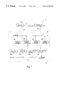
- FIG. 1 is a block diagram of one embodiment of a Time Divisional Multiplexed (TDM) network system of the present invention applied to a modular digital audio system.
- the TDM network system 10 includes a TDM network 20 , base cards 30 A, 30 B, 30 C and 30 D, peripherals 40 A and 40 B, and a system backplane 50 .
- the TDM network 20 , the base cards 30 A- 30 D, and the system bus 50 are contained within a Macintosh II computer, and the backplane 50 consists of a Macintosh NuBus.
- the TDM network and the base cards may be installed in a DigiDesign NuBus expansion chassis manufactured by DigiDesign, Menlo Park, Calif.
- Co-pending application Ser. No. 08/490,457 entitled “SYSTEM AND METHOD FOR PROCESSING DIGITAL AUDIO DATA” provides a further description of the modular digital audio system and is incorporated herein by reference.
- the base cards include sources, destinations, and processors for digital audio signals transmitted over the TDM network.
- the base cards may include functions of audio devices found in a recording studio including equalizers, mixers, synthesizers and samplers.
- Co-pending application Ser. No. 08/490,459 entitled “SYSTEM AND METHOD FOR DISTRIBUTING PROCESSING AMONG A PLURALITY OF DIGITAL SIGNAL PROCESSORS” provides a further description of signal processing in the base cards and is incorporated herein by reference.
- the TDM network 20 consists of network interface modules 22 A, 22 B, 22 C, and 22 D and a TDM bus 24 .
- the TDM bus 24 in one embodiment of the present invention, comprises a multi-connector flexible ribbon cable connected to each of the interface modules.
- Each base card connects to the TDM bus through one of the interface modules.
- the interface modules are shown separate from the base cards. However, in a preferred embodiment, the interface modules are piggy back cards mounted directly on the base cards.
- the interface modules may also be directly incorporated on the base card as discrete components on the base card, as a separate ASIC on the base card, or incorporated within an ASIC particular to the base card's function.
- the peripherals 40 A and 40 B are each shown connected to base cards 30 B and 30 D respectively.
- the peripherals provide the interface for external audio signals to the TDM network system and may include devices such as VCRs, film projectors, and audio tape recorders. In the embodiment shown in FIG. 1, only two peripherals are included in the system. The number of peripherals in a system is variable to meet the requirements of a user.
- the TDM network system shown in FIG. 1 is used to transfer digital audio data from one base card to another.
- the TDM network 20 essentially acts as a patch bay for connecting digital audio signals between base cards of the system.
- the digital audio output from one base card may be provided to an input of one, or more than one, other base cards.
- the TDM network is designed to transfer 256 digital audio signals in real time simultaneously. In order to accomplish real time transfer of 256 digital audio signals, one digital sample of each audio signal is transferred per sample period. In order to transfer 256 digital audio signals in real time, 256 samples are transferred per sample period. Time division multiplexing is used such that the sample period is divided into 256 time slots, and one sample from each of the 256 digital audio signals is transferred in one of the time slots in one sample period. Each sample period corresponds to one bus cycle of the TDM network.
- each base card may access a maximum of 63 input and 63 output channels of the 256 available channels on the network. The set of inbound channels may be entirely different from the set of outbound channels.
- This section describes the system timing in one embodiment of a TDM network system of the present invention.
- the first level of data synchronization identified as system synchronization, ensures that all elements of the system are synchronized to the sample period or bus cycle boundaries.
- the second level of system synchronization identified as TDM bus synchronization, ensures that the network interface modules identify the location of time slot edges within the sample period and identify the currently active time slot.
- a clock master is designated for each synchronization level.
- the TDM bus synchronization clock is triggered by the system synchronization clock, however, the transfer of data across the bus otherwise runs asynchronous to the system synchronization clock.
- peripheral 40 A has been designated as the master peripheral to provide the system synchronization clock.
- Clock signal 256 ⁇ is provided over interconnection 42 to peripheral 40 B.
- Peripheral 40 A divides clock signal 256 ⁇ by eight to provide a clock signal 32 ⁇ .
- the clock signal 32 ⁇ is provided to base card 30 B over interconnection 44 A.
- Base card 30 B is designated as the master base card since it is connected to the peripheral chosen to provide the system synchronization clock.
- peripheral 40 B divides the clock signal 256 ⁇ received from peripheral 40 A by eight to produce a clock signal 32 ⁇ .
- Peripheral 40 B provides the clock signal 32 ⁇ over interconnection 44 B to base card 30 D.
- the master base card 30 B divides the 32 ⁇ signal by 32 to yield a clock signal designated as 1 ⁇ .
- the 1 ⁇ signal is sent to the network interface module 22 B connected to the master base card 30 B.
- the network interface module 22 B, connected to the master base card 30 B, is designated as the master network interface module.
- all the network interface modules have the potential to be the master network interface card, as they all contain the requisite circuitry, but only the network interface module coupled to the master base card will be designated as the master network interface module. All other TDM network interface modules are designated as TDM clock slaves.
- the master network interface card has a crystal on board that operates at 55.1724 MHz. This clock gets divided down to yield two 50% duty cycle clocks at 13.793 MHz that are exactly one-quarter clock cycle apart from each other. These clocks are identified as TDM Ph0 clock and TDM Ph1 clock with the TDM Ph0 clock leading TDM Ph1 clock.
- the Ph0 clock signal is shown in FIG. 2 along with the 1 ⁇ clock signal and a TDM Start signal.
- the TDM Start signal is used to reset slot counters inside the network interface modules at the start of a bus cycle.
- the TDM Start signal is derived from the 1 ⁇ clock, received from the master base card, and the Ph0 clock.
- the TDM Start signal is generated in a preferred embodiment using a TDM Start signal generator circuit shown in FIG. 3 .
- the circuit of FIG. 3 consists of three re-timing flip-flops 60 A, 60 B, and 60 C and a leading edge detector 70 consisting of an and gate 72 and a re-timing flip-flop 74 .
- Re-timing flip-flop 60 A receives the 1 ⁇ clock signal and the Ph0 clock signal.
- a resynchronization of the 1 ⁇ clock to the Ph0 clock is performed in re-timing flip-flops 60 A and 60 B.
- the network interface module uses the 1 ⁇ signal from the master base card as an asynchronous trigger to generate the TDM Start signal to restart the synchronous TDM bus at each sample period.
- the TDM bus is not strictly synchronous to the system clock master.
- the TDM Start signal occurs just after the 1 ⁇ clock signal.
- the 256 ⁇ clock signal in the peripheral has a clock rate that is exactly 256 times greater than the clock rate of the 1 ⁇ clock signal whose period corresponds to the system sample period.
- the Ph0 clock has a clock rate somewhat faster than the rate of the 256 ⁇ clock signal. Therefore, 256 time slots occur in less time than the full sample period.
- the slack time consisting of the difference in time between the 256 time slots and the sample period, is taken up by a variable length idle period, or dead zone, which is inserted between sample period bursts consisting of 256 time slots each. Because of the relationship between the TDM start signal and the Ph0 clock, there is an integer multiple of periods of the clock during the dead zone as shown in FIG. 2 . There are in general a different number of clock periods in the dead zones of successive sample periods, although this number will never vary by more than one clock period from one sample period to the next for a fixed sample period.
- the implementation of the asynchronous/synchronous clock scheme in a preferred embodiment of the present invention described above provides several advantages.
- the number of time slots per sample period may be changed by swapping the crystal used to generate the Ph0 clock in the network interface module for one of lower or higher frequency, as required.
- the network interface module because of this flexibility, can support a wide variety of sample rates without changing the master clock. This allows one system to be used for a wide variety of tasks without architectural changes. In the prior art systems, it is necessary to change the master clock to provide this flexibility since the master clock is synchronous to the sample rate and the TDM slot division.
- the clock scheme also allows a continuously varying system sample period to be used.
- the network interface module is able to adapt to variations in the sample period by varying the length of the dead zone at the end of the sample period.
- the ability to adapt to varying sample rates is particularly useful when the peripheral generating the system clock signal comprises mechanical equipment such as VCRs, film projectors, and audio tape recorders. In these peripherals, it is generally difficult to maintain a completely stable clock.
- the clock instability creates problems in prior art systems that have the sample rate synchronous with the TDM slot divisions and the master clock, both of which are fixed. In prior art systems, if a bus cycle shrinks in time due to clock instability, the length of each of the time slots will also decrease, creating access time violations for devices and memories connected to the bus as the data to and from the bus must be transmitted and received in less time.
- instabilities of the system clock are transparent to the client as the network interface module will adjust for variations in the sample clock by increasing or decreasing the length of the dead zone.
- the length of each time slot remains constant despite variations in the sample clock.
- the number of time slots per bus cycle may be reduced, but the length of the time slots remains constant. This allows for the sample rate to drift and the bus to remain synchronous with the mechanical equipment.
- each of the interface network modules has an internal register, designated as max count, which may be programmed for any different number (designated as the max count value) of time slots per sample period.
- Internal counters in the network interface module start counting synchronously with the Ph0 clock upon receipt of the TDM start signal. These counters stop counting once they reach the max count value, and remain at the max count value for the duration of the dead zone. Upon arrival of the next TDM start pulse, the counters again begin counting from zero. These counters provide the ability to vary the number of time slots per sample period by changing only the programmed max count value.
- the three timing signals generated in the network interface card, Ph0 clock, Ph1 clock, and TDM start, as well as the 1 ⁇ clock generated in the master data bus card, a 2 ⁇ clock generated in the master data bus card, and the 32 ⁇ clock received from the peripheral, are transmitted over the network bus to each of the interface network cards.
- Each network interface card drives its output data to the bus at the rising edge of the Ph0 clock.
- the receiving network interface card uses the falling edge of the Ph1 clock to latch in data from the network. This ensures that there is no danger of missing data due to clock skew depending on data transmission direction out on the bus.
- the network interface modules 22 A- 22 D provide the interface to the TDM bus 24 for each node of the TDM network.
- Each network interface module acts as a node controller for the node of the network.
- a block diagram of a network interface module 22 in accordance with one embodiment of the present inventions is shown in FIG. 4 .
- the network interface module includes a TDM ASIC pair 200 comprised of TDM ASICS 210 A and 210 B, a client connector 220 , a TDM bus connector 230 , TDM buffers 270 A and 270 B, an internal TDM bus 260 , and a clock circuit 240 .
- the clock circuit 240 performs the network interface module clocking functions described above under the overall system timing description.
- FIG. 5 shows the clock circuit 240 in greater detail, as well as the individual clock connections between the client, the network interface module, and the TDM network cable.
- the clock circuit 240 includes a 55.1724 MHz crystal circuit 242 , a divide by 4 circuit 244 and a re-timing circuit 246 .
- the re-timing circuit includes the TDM Start signal generator circuit 80 discussed previously with reference to FIG. 3 .
- a network interface module has the capability to provide six clocks out the TDM ribbon cable. Three of the clocks (1 ⁇ , 2 ⁇ and 32 ⁇ ) are related to system synchronization, and are provided from the master base card.
- the other three clocks (Ph0 clock, Ph1 clock, and TDM start) provide TDM bus synchronization and are generated on the master network interface module.
- the three TDM clocks are provided out on the bus only by the master network interface module, but are received by all of the network interface modules on the bus.
- the audio samples are comprised of 24 bits.
- outbound data from the client is received at the client connector 220 and is transferred to the TDM ASIC pair 200 . Twelve most significant bits of the outbound data are transferred to TDM ASIC 210 A and twelve least significant bits of the outbound data are transferred to TDM ASIC 210 B.
- the outbound data is transferred from the TDM ASIC pair 210 over an internal TDM bus 260 to the outbound TDM buffer 270 A for transfer over the TDM bus through the TDM connector 230 .
- inbound data received from the TDM bus, is temporarily stored in TDM inbound buffer 270 B, and then transferred over the internal TDM bus 260 to the TDM ASIC pair 200 where the twelve most significant bits are transferred to TDM ASIC 210 A and the twelve least significant bits are transferred to TDM ASIC 210 B.
- the inbound data is then transferred through the client connector 220 to the client.
- a general functional description of one embodiment of a network interface module in accordance with the present invention has been provided above. A detailed description of the TDM ASIC pair of one embodiment of the present invention is further described below.
- two identical ASICs are used in the network interface module. Each of the ASICs perform identical functions for 12 bits of the 24 bit audio data words. It should be understood that the present invention is not limited to the embodiment described using two ASICs. Those skilled in the art will recognize that only one ASIC, or more than two ASICs could be used in the network interface module to provide the functions of the pair of ASICs in the illustrative embodiment. Also, the components contained within the ASICs may be provided as discrete components.
- FIG. 6 shows the TDM architecture of each of the TDM ASICS 210 A and 210 B shown in FIG. 4 .
- Each TDM ASIC includes an SRAM 310 comprised of two pages 312 and 314 , a slot counter 316 , an indirection register 326 , MUXes 318 - 326 , a register file 332 containing data registers, and a control circuit 330 .
- each TDM ASIC includes a slot counter 316 .
- the slot counter is set to zero at the start of each new bus cycle and is incremented by the TDM bus slot clock Ph0 so that the slot counter always has a value corresponding to the active time slot of the TDM network.
- the indirection register 328 in a preferred embodiment comprises a 256 ⁇ 8indirection SRAM and functions as a slot assignment table.
- the slot assignment table is preprogrammed with values corresponding to the channels of the 256 network channels that are designated as inbound and outbound channels for the client connected to the network interface module comprising the ASIC.
- the slot assignment table also contains addressing information for mapping each designated channel of the client to a corresponding location in the memory 310 .
- the core of the TDM ASIC is the memory 310 .
- the two pages of the memory 312 and 314 are shared on a 50% duty cycle between a client interface and a TDM bus interface. From the client interface, the memory appears as a double buffer that is page swapped every sample period of the TDM bus. From the TDM bus interface, the memory also appears as a double buffer, except that the TDM bus interface always accesses the page opposite the one that the client is accessing.
- Each page of the memory is divided into an outbound RAM and an inbound RAM as shown in FIG. 7, creating four physical RAM blocks 312 A, 312 B, 314 A, and 314 B.
- outbound data from the client is written to memory block 312 A of page 0
- outbound data is read from memory block 314 A and transmitted out on the TDM bus
- inbound data is written into memory block 314 B from the TDM bus
- inbound data is read from the memory block 312 B and transferred to the client.
- Page 1 now provides the client interface and page 0 provides the TDM interface.
- the outbound data that was stored in block 312 A in the previous bus cycle is read from memory block 312 A and transmitted out on the data bus, the inbound data that was read into memory block 314 B in the previous bus cycle is transferred to the client, a new set of outbound data is written into memory block 314 A from the client and a new set of inbound data is from the TDM bus is written into memory block 312 B.
- the physical blocks of memory inside the TDM ASIC are not permanently assigned to either the TDM interface or the client interface. Their assignment switches with each bus cycle.
- the MUXes 318 - 324 along with the slot assignment table and the slot counter 316 are used to control the flow of data to and from the memory 310 to ensure that data is written to, and read from, the proper memory locations.
- the register file 332 , the control circuit 330 and the mux 326 are used in a FIFO mode of the ASIC described further below.
- the register file 332 is used to store prefetched data samples under the control of the control circuit 330 .
- the mux 326 responsive to a mode control signal, provides the client with either the prefetched data samples or data from the memory 310 .
- the client is oblivious to the fact that there are four physical blocks of RAM inside the TDM ASIC.
- the client uses the same address base to access what it sees as a single RAM, addressed by channel number, containing multiple inbound and outbound channels.
- the client may write a new set of audio samples into the RAM every sample period, and it may read a different set of audio samples out of the TDM ASIC every sample period.
- the client can write and read to the memory.
- the memory 310 appears as regular random access memory.
- the memory is read by the client by providing an address to the memory, and receiving the data stored in the location corresponding to that address.
- the second mode reduces the read access time of the inbound audio data.
- FIFO mode two reads for a second bus cycle are prefetched during the dead zone at the end of a first bus cycle.
- the data corresponding to the addresses of the first two reads are stored in a first register and a second register contained within the register file 332 .
- RAM access time does not impede the timing of the read.
- the first read triggers a third internal read which begins immediately and continues after the client has gone away. Data from the second register is transferred into the first register, and data corresponding to the third read is stored in the second register.
- the data for the second read is available in the first buffer, and the second read triggers the next internal read.
- the write timing does not benefit from the FIFO mode in the same way, however, the write addresses can be precalculated so that a write takes less time to occur than in normal random access mode.
- the slot assignment table can be programmed so that the mapping of the TDM time slots in the memory reorders or groups the time slots for random and sequential access. This is also useful for FIFO mode where access to the data in FIFO form is desired but the data is not contained within contiguous or sequential time slots.
- Random access mode is important in distributed systems where there is no guarantee that the client will have access to the data in sequential order and may only know where the data is located in the RAM.
- the data is only supplied in time slot order which limits the type of processing algorithms that the client can run. For example, when a client is running multiple DSP algorithms on multiple data streams, it is highly unlikely that the data needed for algorithm no. 1 will appear before the data needed for algorithm no. 2 and so on. The data would most likely not be sequential or adjacent but scrambled and separated by other data used for other processing functions or by other clients for their own algorithms.
- indirection table along with random access mode alleviates the problem of prior art systems described above.
- Data stored in the memory can be grouped according to algorithm or client (in the case where the node controller is shared). Once the indirection table is created, it is transparent to the client what time slot is being read from or written to. The client only knows that it is accessing data at a particular address in the RAM.
- the FIFO mode is particularly useful for clients utilizing algorithms that require fast sequential access or where a great deal of data needs to be processed as fast as possible.
- the FIFO mode along with the indirection table allows extremely fast data access.
- the indirection table can be used to map to what appears to be sequential locations in the memory, that can be a accessed through FIFO mode. This allows a client to have extremely fast access to very different and random locations in the memory.
- the network comprises 256 channels and each network interface module provides a client access to 63 of the channels for inbound data and 63 of the channels for outbound data. It should be understood that the invention is applicable to networks having a number of channels other than 256, and for clients having access to a number of channels other than 126. Also, multiple clients can be supported from one network interface module, with each of the multiple clients being assigned a subset of the channels assigned to the network interface module.
Abstract
Description
Claims (32)
Priority Applications (1)
| Application Number | Priority Date | Filing Date | Title |
|---|---|---|---|
| US08/556,442 US6212197B1 (en) | 1995-06-14 | 1995-11-09 | Apparatus and method for accessing memory in a TDM network |
Applications Claiming Priority (2)
| Application Number | Priority Date | Filing Date | Title |
|---|---|---|---|
| US08/490,461 US6072796A (en) | 1995-06-14 | 1995-06-14 | Apparatus and method for accessing memory in a TDM network |
| US08/556,442 US6212197B1 (en) | 1995-06-14 | 1995-11-09 | Apparatus and method for accessing memory in a TDM network |
Related Parent Applications (1)
| Application Number | Title | Priority Date | Filing Date |
|---|---|---|---|
| US08/490,461 Continuation US6072796A (en) | 1995-06-14 | 1995-06-14 | Apparatus and method for accessing memory in a TDM network |
Publications (1)
| Publication Number | Publication Date |
|---|---|
| US6212197B1 true US6212197B1 (en) | 2001-04-03 |
Family
ID=23948154
Family Applications (2)
| Application Number | Title | Priority Date | Filing Date |
|---|---|---|---|
| US08/490,461 Expired - Fee Related US6072796A (en) | 1995-06-14 | 1995-06-14 | Apparatus and method for accessing memory in a TDM network |
| US08/556,442 Expired - Lifetime US6212197B1 (en) | 1995-06-14 | 1995-11-09 | Apparatus and method for accessing memory in a TDM network |
Family Applications Before (1)
| Application Number | Title | Priority Date | Filing Date |
|---|---|---|---|
| US08/490,461 Expired - Fee Related US6072796A (en) | 1995-06-14 | 1995-06-14 | Apparatus and method for accessing memory in a TDM network |
Country Status (1)
| Country | Link |
|---|---|
| US (2) | US6072796A (en) |
Cited By (17)
| Publication number | Priority date | Publication date | Assignee | Title |
|---|---|---|---|---|
| US20030174724A1 (en) * | 2002-03-15 | 2003-09-18 | Lockheed Martin Corporation | Synchronous low voltage differential I/O buss |
| US6636100B1 (en) * | 1999-06-29 | 2003-10-21 | Mitsubishi Denki Kabushiki Kaisha | Can controller and one-chip computer having a built-in can controller |
| US7031305B1 (en) * | 1999-05-24 | 2006-04-18 | Advanced Micro Devices, Inc. | Apparatus and method for programmable memory access slot assignment |
| US7050450B1 (en) * | 1998-08-28 | 2006-05-23 | Siemens Aktiengesellschaft | Telecommunications system and method for producing a master clock in the same |
| US20060200785A1 (en) * | 2003-01-17 | 2006-09-07 | Drazen Borkovic | Method and apparatus for the design and analysis of digital circuits with time division multiplexing |
| US20070050062A1 (en) * | 2005-08-26 | 2007-03-01 | Estes Christopher A | Closed loop analog signal processor ("clasp") system |
| US20100296673A1 (en) * | 2005-08-26 | 2010-11-25 | Endless Analog, Inc. | Closed Loop Analog Signal Processor ("CLASP") System |
| US9070408B2 (en) | 2005-08-26 | 2015-06-30 | Endless Analog, Inc | Closed loop analog signal processor (“CLASP”) system |
| US11271874B2 (en) | 2020-02-05 | 2022-03-08 | Mellanox Technologies, Ltd. | Network adapter with time-aware packet-processing pipeline |
| US11336383B2 (en) | 2020-06-24 | 2022-05-17 | Mellanox Technologies, Ltd. | Packet scheduling system with desired physical transmission time for packets |
| US11388263B2 (en) | 2020-10-11 | 2022-07-12 | Mellanox Technologies, Ltd. | Packet transmission using scheduled prefetching |
| US11476928B2 (en) | 2020-03-18 | 2022-10-18 | Mellanox Technologies, Ltd. | TDMA networking using commodity NIC/switch |
| US11711158B2 (en) | 2021-06-28 | 2023-07-25 | Mellanox Technologies, Ltd. | Accurate time-stamping of outbound packets |
| US11876885B2 (en) | 2020-07-02 | 2024-01-16 | Mellanox Technologies, Ltd. | Clock queue with arming and/or self-arming features |
| US11876642B2 (en) | 2019-02-25 | 2024-01-16 | Mellanox Technologies, Ltd. | Collective communication system and methods |
| US11880711B2 (en) | 2020-12-14 | 2024-01-23 | Mellanox Technologies, Ltd. | Offloading execution of a multi-task parameter-dependent operation to a network device |
| US11922237B1 (en) | 2022-09-12 | 2024-03-05 | Mellanox Technologies, Ltd. | Single-step collective operations |
Families Citing this family (31)
| Publication number | Priority date | Publication date | Assignee | Title |
|---|---|---|---|---|
| US5845313A (en) | 1995-07-31 | 1998-12-01 | Lexar | Direct logical block addressing flash memory mass storage architecture |
| US6978342B1 (en) | 1995-07-31 | 2005-12-20 | Lexar Media, Inc. | Moving sectors within a block of information in a flash memory mass storage architecture |
| US8171203B2 (en) | 1995-07-31 | 2012-05-01 | Micron Technology, Inc. | Faster write operations to nonvolatile memory using FSInfo sector manipulation |
| US6728851B1 (en) * | 1995-07-31 | 2004-04-27 | Lexar Media, Inc. | Increasing the memory performance of flash memory devices by writing sectors simultaneously to multiple flash memory devices |
| US5666390A (en) * | 1995-09-28 | 1997-09-09 | Micron Technology, Inc. | High speed programmable counter |
| US7072330B2 (en) * | 1998-04-03 | 2006-07-04 | Consolidated Ip Holdings, Inc. | Systems for voice and data communications having TDM and packet buses and telephony station cards including voltage generators |
| US6498791B2 (en) | 1998-04-03 | 2002-12-24 | Vertical Networks, Inc. | Systems and methods for multiple mode voice and data communications using intelligently bridged TDM and packet buses and methods for performing telephony and data functions using the same |
| US6389009B1 (en) | 2000-12-28 | 2002-05-14 | Vertical Networks, Inc. | Systems and methods for multiple mode voice and data communications using intelligently bridged TDM and packet buses |
| US6154465A (en) * | 1998-10-06 | 2000-11-28 | Vertical Networks, Inc. | Systems and methods for multiple mode voice and data communications using intelligenty bridged TDM and packet buses and methods for performing telephony and data functions using the same |
| US6181694B1 (en) | 1998-04-03 | 2001-01-30 | Vertical Networks, Inc. | Systems and methods for multiple mode voice and data communciations using intelligently bridged TDM and packet buses |
| US20090059818A1 (en) * | 1998-04-03 | 2009-03-05 | Pickett Scott K | Systems and methods for providing configurable caller id iformation |
| US6847650B1 (en) * | 2000-06-29 | 2005-01-25 | Sony Corporation | System and method for utilizing a memory device to support isochronous processes |
| US7167944B1 (en) | 2000-07-21 | 2007-01-23 | Lexar Media, Inc. | Block management for mass storage |
| NO20006185L (en) * | 2000-12-05 | 2002-06-06 | Ericsson Telefon Ab L M | Method and arrangement for synchronizing a TDM bus |
| US7187673B2 (en) * | 2000-12-18 | 2007-03-06 | Koninklijke Philips Electronics N.V. | Technique for creating a machine to route non-packetized digital signals using distributed RAM |
| GB0123410D0 (en) | 2001-09-28 | 2001-11-21 | Memquest Ltd | Memory system for data storage and retrieval |
| GB0123415D0 (en) | 2001-09-28 | 2001-11-21 | Memquest Ltd | Method of writing data to non-volatile memory |
| GB0123421D0 (en) | 2001-09-28 | 2001-11-21 | Memquest Ltd | Power management system |
| GB0123416D0 (en) | 2001-09-28 | 2001-11-21 | Memquest Ltd | Non-volatile memory control |
| GB0123417D0 (en) * | 2001-09-28 | 2001-11-21 | Memquest Ltd | Improved data processing |
| US7231643B1 (en) | 2002-02-22 | 2007-06-12 | Lexar Media, Inc. | Image rescue system including direct communication between an application program and a device driver |
| US7869424B2 (en) * | 2002-07-01 | 2011-01-11 | Converged Data Solutions Inc. | Systems and methods for voice and data communications including a scalable TDM switch/multiplexer |
| US7706359B2 (en) * | 2002-07-01 | 2010-04-27 | Converged Data Solutions, Inc. | Systems and methods for voice and data communications including a network drop and insert interface for an external data routing resource |
| US6804504B1 (en) * | 2002-08-23 | 2004-10-12 | Innovative Electronic Designs, Inc. | Audio processing system |
| US7725628B1 (en) | 2004-04-20 | 2010-05-25 | Lexar Media, Inc. | Direct secondary device interface by a host |
| US7370166B1 (en) | 2004-04-30 | 2008-05-06 | Lexar Media, Inc. | Secure portable storage device |
| US7464306B1 (en) | 2004-08-27 | 2008-12-09 | Lexar Media, Inc. | Status of overall health of nonvolatile memory |
| US7594063B1 (en) | 2004-08-27 | 2009-09-22 | Lexar Media, Inc. | Storage capacity status |
| US20070027485A1 (en) * | 2005-07-29 | 2007-02-01 | Kallmyer Todd A | Implantable medical device bus system and method |
| US7882307B1 (en) | 2006-04-14 | 2011-02-01 | Tilera Corporation | Managing cache memory in a parallel processing environment |
| EP2422452A4 (en) * | 2009-04-24 | 2013-07-24 | Nokia Corp | Data rearrangement for decoder |
Citations (20)
| Publication number | Priority date | Publication date | Assignee | Title |
|---|---|---|---|---|
| US4224688A (en) | 1978-10-30 | 1980-09-23 | Northern Telecom Limited | Digital conference circuit |
| US4271502A (en) | 1979-06-19 | 1981-06-02 | Magnavox Government And Industrial Electronics Co. | Digital voice conferencer |
| US4575845A (en) | 1984-09-06 | 1986-03-11 | At&T Bell Laboratories | Time division multiplex conferencer |
| US4646288A (en) | 1985-01-31 | 1987-02-24 | Denro Laboratories, Inc. | Multi-line accumulator/multiplexer |
| US4797877A (en) | 1986-12-18 | 1989-01-10 | American Telephone And Telegraph Company | Communication system dynamic conferencer circuit |
| US4819228A (en) * | 1984-10-29 | 1989-04-04 | Stratacom Inc. | Synchronous packet voice/data communication system |
| US5027347A (en) | 1988-06-10 | 1991-06-25 | Heikki Malkki | Intercom system |
| US5165023A (en) * | 1986-12-17 | 1992-11-17 | Massachusetts Institute Of Technology | Parallel processing system with processor array and network communications system for transmitting messages of variable length |
| US5197065A (en) * | 1989-09-26 | 1993-03-23 | International Business Machines Corporation | Distribution mechanism for establishing communications between user interfaces of a communication system |
| US5235594A (en) * | 1991-08-09 | 1993-08-10 | Westinghouse Electric Corp. | Time division multiplex voice data bus |
| US5255264A (en) * | 1991-09-26 | 1993-10-19 | Ipc Information Systems, Inc. | Distributed control switching network for multi-line telephone communications |
| US5280482A (en) * | 1991-06-17 | 1994-01-18 | Dainippon Screen Mfg. Co., Ltd. | Time-sharing data transfer apparatus |
| US5317693A (en) * | 1991-04-04 | 1994-05-31 | Digital Equipment Corporation | Computer peripheral device network with peripheral address resetting capabilities |
| US5357511A (en) | 1993-03-22 | 1994-10-18 | Peak Audio, Inc. | Distributed processing in a digital audio mixing network |
| US5381413A (en) * | 1992-12-28 | 1995-01-10 | Starlight Networks | Data throttling system for a communications network |
| US5402388A (en) * | 1993-12-16 | 1995-03-28 | Mosaid Technologies Incorporated | Variable latency scheme for synchronous memory |
| US5432782A (en) * | 1991-07-23 | 1995-07-11 | Kabushiki Kaisha Toshiba | Packet switching system |
| US5526344A (en) * | 1994-04-15 | 1996-06-11 | Dsc Communications Corporation | Multi-service switch for a telecommunications network |
| US5530963A (en) * | 1993-12-16 | 1996-06-25 | International Business Machines Corporation | Method and system for maintaining routing between mobile workstations and selected network workstation using routing table within each router device in the network |
| US5588004A (en) * | 1994-09-07 | 1996-12-24 | Hitachi, Ltd. | Bus synchronizing method and system based thereon |
Family Cites Families (4)
| Publication number | Priority date | Publication date | Assignee | Title |
|---|---|---|---|---|
| US4143241A (en) * | 1977-06-10 | 1979-03-06 | Bell Telephone Laboratories, Incorporated | Small digital time division switching arrangement |
| US4254498A (en) * | 1978-02-01 | 1981-03-03 | Nippon Telegraph And Telephone Public Corporation | Time division telephone switching systems |
| US5123012A (en) * | 1989-06-06 | 1992-06-16 | Mitsubishi Denki Kabushiki Kaisha | Time division switching apparatus |
| US5260937A (en) * | 1990-10-29 | 1993-11-09 | Dsc Communications Corporation | Power conserving technique for a communications terminal time slot interchanger |
-
1995
- 1995-06-14 US US08/490,461 patent/US6072796A/en not_active Expired - Fee Related
- 1995-11-09 US US08/556,442 patent/US6212197B1/en not_active Expired - Lifetime
Patent Citations (20)
| Publication number | Priority date | Publication date | Assignee | Title |
|---|---|---|---|---|
| US4224688A (en) | 1978-10-30 | 1980-09-23 | Northern Telecom Limited | Digital conference circuit |
| US4271502A (en) | 1979-06-19 | 1981-06-02 | Magnavox Government And Industrial Electronics Co. | Digital voice conferencer |
| US4575845A (en) | 1984-09-06 | 1986-03-11 | At&T Bell Laboratories | Time division multiplex conferencer |
| US4819228A (en) * | 1984-10-29 | 1989-04-04 | Stratacom Inc. | Synchronous packet voice/data communication system |
| US4646288A (en) | 1985-01-31 | 1987-02-24 | Denro Laboratories, Inc. | Multi-line accumulator/multiplexer |
| US5165023A (en) * | 1986-12-17 | 1992-11-17 | Massachusetts Institute Of Technology | Parallel processing system with processor array and network communications system for transmitting messages of variable length |
| US4797877A (en) | 1986-12-18 | 1989-01-10 | American Telephone And Telegraph Company | Communication system dynamic conferencer circuit |
| US5027347A (en) | 1988-06-10 | 1991-06-25 | Heikki Malkki | Intercom system |
| US5197065A (en) * | 1989-09-26 | 1993-03-23 | International Business Machines Corporation | Distribution mechanism for establishing communications between user interfaces of a communication system |
| US5317693A (en) * | 1991-04-04 | 1994-05-31 | Digital Equipment Corporation | Computer peripheral device network with peripheral address resetting capabilities |
| US5280482A (en) * | 1991-06-17 | 1994-01-18 | Dainippon Screen Mfg. Co., Ltd. | Time-sharing data transfer apparatus |
| US5432782A (en) * | 1991-07-23 | 1995-07-11 | Kabushiki Kaisha Toshiba | Packet switching system |
| US5235594A (en) * | 1991-08-09 | 1993-08-10 | Westinghouse Electric Corp. | Time division multiplex voice data bus |
| US5255264A (en) * | 1991-09-26 | 1993-10-19 | Ipc Information Systems, Inc. | Distributed control switching network for multi-line telephone communications |
| US5381413A (en) * | 1992-12-28 | 1995-01-10 | Starlight Networks | Data throttling system for a communications network |
| US5357511A (en) | 1993-03-22 | 1994-10-18 | Peak Audio, Inc. | Distributed processing in a digital audio mixing network |
| US5402388A (en) * | 1993-12-16 | 1995-03-28 | Mosaid Technologies Incorporated | Variable latency scheme for synchronous memory |
| US5530963A (en) * | 1993-12-16 | 1996-06-25 | International Business Machines Corporation | Method and system for maintaining routing between mobile workstations and selected network workstation using routing table within each router device in the network |
| US5526344A (en) * | 1994-04-15 | 1996-06-11 | Dsc Communications Corporation | Multi-service switch for a telecommunications network |
| US5588004A (en) * | 1994-09-07 | 1996-12-24 | Hitachi, Ltd. | Bus synchronizing method and system based thereon |
Non-Patent Citations (6)
| Title |
|---|
| An Audio Engineering Society Preprint, Presented at the 78th Convention May 3-6, 1895 Anaheim, "The Digital Audio Processing Station: A New Concept in Audio Post-Production", James A. Moorer et al, 2242 (D-4). |
| An Audio Engineering Society Preprint, Presented at the 83rd Convention Oct. 16-19, 1987 New York, "A Magnetic Storage Disk-Based Digital Audio Recording, Editing, and Processing System", Charles L. Bagnaschi, 2505 (H-3). |
| An Audio Engineering Society Preprint, Presented at the 89th Convention 1990 Sep. 21-25, Los Angeles, "Optimizing Massive Parallel Architectures for Real-Time Digital Audio", Ken N. Linton et al., Preprint #2972, Session-Paper#F-II-6. |
| An Audio Engineering Society Preprint, Presented at the 95th Convention Oct. 7-10, 1993 New York, "An Object Oriented System for Digital Audio Workstation DSP Development", Theodore C. Tanner, Jr. et al., 3754 (B3-PM-1). |
| Principles of Digital Audio, Second Edition, Eighth Printing-1994, Ken C. Pohlmann. |
| Principles of Digital Audio, Second Edition, Eighth Printing—1994, Ken C. Pohlmann. |
Cited By (22)
| Publication number | Priority date | Publication date | Assignee | Title |
|---|---|---|---|---|
| US7050450B1 (en) * | 1998-08-28 | 2006-05-23 | Siemens Aktiengesellschaft | Telecommunications system and method for producing a master clock in the same |
| US7031305B1 (en) * | 1999-05-24 | 2006-04-18 | Advanced Micro Devices, Inc. | Apparatus and method for programmable memory access slot assignment |
| US6636100B1 (en) * | 1999-06-29 | 2003-10-21 | Mitsubishi Denki Kabushiki Kaisha | Can controller and one-chip computer having a built-in can controller |
| US7315551B2 (en) * | 2002-03-15 | 2008-01-01 | Lockheed Martin Corporation | Synchronous low voltage differential I/O buss |
| US20030174724A1 (en) * | 2002-03-15 | 2003-09-18 | Lockheed Martin Corporation | Synchronous low voltage differential I/O buss |
| US8479142B2 (en) * | 2003-01-17 | 2013-07-02 | Synopsys, Inc. | Method and apparatus for the design and analysis of digital circuits with time division multiplexing |
| US20060200785A1 (en) * | 2003-01-17 | 2006-09-07 | Drazen Borkovic | Method and apparatus for the design and analysis of digital circuits with time division multiplexing |
| US8726219B2 (en) | 2003-01-17 | 2014-05-13 | Synopsys, Inc. | Analysis of digital circuits with time division multiplexing |
| US8630727B2 (en) | 2005-08-26 | 2014-01-14 | Endless Analog, Inc | Closed loop analog signal processor (“CLASP”) system |
| US20100296673A1 (en) * | 2005-08-26 | 2010-11-25 | Endless Analog, Inc. | Closed Loop Analog Signal Processor ("CLASP") System |
| US7751916B2 (en) | 2005-08-26 | 2010-07-06 | Endless Analog, Inc. | Closed loop analog signal processor (“CLASP”) system |
| US20070050062A1 (en) * | 2005-08-26 | 2007-03-01 | Estes Christopher A | Closed loop analog signal processor ("clasp") system |
| US9070408B2 (en) | 2005-08-26 | 2015-06-30 | Endless Analog, Inc | Closed loop analog signal processor (“CLASP”) system |
| US11876642B2 (en) | 2019-02-25 | 2024-01-16 | Mellanox Technologies, Ltd. | Collective communication system and methods |
| US11271874B2 (en) | 2020-02-05 | 2022-03-08 | Mellanox Technologies, Ltd. | Network adapter with time-aware packet-processing pipeline |
| US11476928B2 (en) | 2020-03-18 | 2022-10-18 | Mellanox Technologies, Ltd. | TDMA networking using commodity NIC/switch |
| US11336383B2 (en) | 2020-06-24 | 2022-05-17 | Mellanox Technologies, Ltd. | Packet scheduling system with desired physical transmission time for packets |
| US11876885B2 (en) | 2020-07-02 | 2024-01-16 | Mellanox Technologies, Ltd. | Clock queue with arming and/or self-arming features |
| US11388263B2 (en) | 2020-10-11 | 2022-07-12 | Mellanox Technologies, Ltd. | Packet transmission using scheduled prefetching |
| US11880711B2 (en) | 2020-12-14 | 2024-01-23 | Mellanox Technologies, Ltd. | Offloading execution of a multi-task parameter-dependent operation to a network device |
| US11711158B2 (en) | 2021-06-28 | 2023-07-25 | Mellanox Technologies, Ltd. | Accurate time-stamping of outbound packets |
| US11922237B1 (en) | 2022-09-12 | 2024-03-05 | Mellanox Technologies, Ltd. | Single-step collective operations |
Also Published As
| Publication number | Publication date |
|---|---|
| US6072796A (en) | 2000-06-06 |
Similar Documents
| Publication | Publication Date | Title |
|---|---|---|
| US6212197B1 (en) | Apparatus and method for accessing memory in a TDM network | |
| US6226338B1 (en) | Multiple channel data communication buffer with single transmit and receive memories | |
| US5351043A (en) | Queueing protocol | |
| US4797589A (en) | Dynamically reconfigurable time-space-time digital switch and network | |
| CA2185698A1 (en) | High-speed switched network architecture | |
| US5625796A (en) | Method and apparatus for concurrently accessing multiple memories with different timing requirements | |
| US4993026A (en) | Multiplexer apparatus with auxiliary synchronization for compensating for cable delays | |
| JPH02260993A (en) | Parallel time slot exchanging matrix and switching module used for it | |
| CA1212743A (en) | Digital transmission systems | |
| US6067296A (en) | Parallel backplane architecture providing asymmetric bus time slot cross-connect capability | |
| JPH0523530B2 (en) | ||
| US5832216A (en) | Network adapter having single ported memory which is accessible by network and peripheral bus on a time division multiplexed (TDM) basis | |
| EP1384357B1 (en) | Architectures for a single-stage switch | |
| JP2677670B2 (en) | Crossing circuit between two buses | |
| US5708850A (en) | Parallel processing system for time division multiplex data transfer including read/write dual port memory accessible to bus and digital signal processor during opposite phases of clock | |
| JPS5917596B2 (en) | Time division channel switch circuit | |
| JPH05191441A (en) | System for processing synchronized time-division signal like non-synchronized time-division data packet | |
| JPS6085657A (en) | Multifrequency signal supplying device and method therefor | |
| US5164940A (en) | Modular communication system with allocatable bandwidth | |
| JPH0750648A (en) | Multiple channels asynchronous signal multiplex transmitter | |
| JPH0744522B2 (en) | Phase synchronization circuit | |
| JPS6123707B2 (en) | ||
| JPH01176197A (en) | Time division multiple access exchange system | |
| JPS59228497A (en) | Time division multi-access multiplexer | |
| GB2286099A (en) | Modular communication system with allocatable bandwidth |
Legal Events
| Date | Code | Title | Description |
|---|---|---|---|
| AS | Assignment |
Owner name: DIGIDESIGN, INC., CALIFORNIA Free format text: ASSIGNMENT OF ASSIGNORS INTEREST;ASSIGNORS:JASMIN, JAMES;CLEMENTSON, DAVID D.;REEL/FRAME:008161/0566 Effective date: 19951127 |
|
| AS | Assignment |
Owner name: AVID TECHNOLOGY, INC., MASSACHUSETTS Free format text: MERGER;ASSIGNOR:DIGIDESIGN, INC.;REEL/FRAME:009790/0510 Effective date: 19951231 |
|
| STCF | Information on status: patent grant |
Free format text: PATENTED CASE |
|
| CC | Certificate of correction | ||
| CC | Certificate of correction | ||
| FPAY | Fee payment |
Year of fee payment: 4 |
|
| FPAY | Fee payment |
Year of fee payment: 8 |
|
| AS | Assignment |
Owner name: WELLS FARGO CAPITAL FINANCE, LLC, AS AGENT, MASSAC Free format text: SECURITY AGREEMENT;ASSIGNORS:AVID TECHNOLOGY, INC.;PINNACLE SYSTEMS, INC.;REEL/FRAME:025675/0413 Effective date: 20101001 |
|
| FPAY | Fee payment |
Year of fee payment: 12 |
|
| AS | Assignment |
Owner name: KEYBANK NATIONAL ASSOCIATION, AS THE ADMINISTRATIV Free format text: PATENT SECURITY AGREEMENT;ASSIGNOR:AVID TECHNOLOGY, INC.;REEL/FRAME:036008/0824 Effective date: 20150622 |
|
| AS | Assignment |
Owner name: AVID SYSTEMS, INC., MASSACHUSETTS Free format text: RELEASE BY SECURED PARTY;ASSIGNOR:WELLS FARGO CAPITAL FINANCE, LLC;REEL/FRAME:036037/0693 Effective date: 20150622 Owner name: AVID TECHNOLOGY INC., MASSACHUSETTS Free format text: RELEASE BY SECURED PARTY;ASSIGNOR:WELLS FARGO CAPITAL FINANCE, LLC;REEL/FRAME:036037/0693 Effective date: 20150622 |
|
| AS | Assignment |
Owner name: AVID TECHNOLOGY, INC., MASSACHUSETTS Free format text: RELEASE OF SECURITY INTEREST IN UNITED STATES PATENTS;ASSIGNOR:KEYBANK NATIONAL ASSOCIATION;REEL/FRAME:037970/0201 Effective date: 20160226 |