US6204832B1 - Image display with lens array scanning relative to light source array - Google Patents

Image display with lens array scanning relative to light source array Download PDF

Info

Publication number
US6204832B1
US6204832B1 US09/072,012 US7201298A US6204832B1 US 6204832 B1 US6204832 B1 US 6204832B1 US 7201298 A US7201298 A US 7201298A US 6204832 B1 US6204832 B1 US 6204832B1
Authority
US
United States
Prior art keywords
image
light
array
microlens
axis
Prior art date
Legal status (The legal status is an assumption and is not a legal conclusion. Google has not performed a legal analysis and makes no representation as to the accuracy of the status listed.)
Expired - Lifetime
Application number
US09/072,012
Inventor
Charles D. Melville
Michael Tidwell
Richard S. Johnston
Current Assignee (The listed assignees may be inaccurate. Google has not performed a legal analysis and makes no representation or warranty as to the accuracy of the list.)
University of Washington
Original Assignee
University of Washington
Priority date (The priority date is an assumption and is not a legal conclusion. Google has not performed a legal analysis and makes no representation as to the accuracy of the date listed.)
Filing date
Publication date
Application filed by University of Washington filed Critical University of Washington
Priority to US09/072,012 priority Critical patent/US6204832B1/en
Assigned to WASHINGTON, UNIVERSITY OF reassignment WASHINGTON, UNIVERSITY OF ASSIGNMENT OF ASSIGNORS INTEREST (SEE DOCUMENT FOR DETAILS). Assignors: MELVILLE, CHARLES D., TIDWELL, MICHAEL, JOHNSTON, RICHARD S.
Application granted granted Critical
Publication of US6204832B1 publication Critical patent/US6204832B1/en
Anticipated expiration legal-status Critical
Expired - Lifetime legal-status Critical Current

Links

Images

Classifications

    • GPHYSICS
    • G09EDUCATION; CRYPTOGRAPHY; DISPLAY; ADVERTISING; SEALS
    • G09GARRANGEMENTS OR CIRCUITS FOR CONTROL OF INDICATING DEVICES USING STATIC MEANS TO PRESENT VARIABLE INFORMATION
    • G09G3/00Control arrangements or circuits, of interest only in connection with visual indicators other than cathode-ray tubes
    • G09G3/007Use of pixel shift techniques, e.g. by mechanical shift of the physical pixels or by optical shift of the perceived pixels
    • GPHYSICS
    • G09EDUCATION; CRYPTOGRAPHY; DISPLAY; ADVERTISING; SEALS
    • G09GARRANGEMENTS OR CIRCUITS FOR CONTROL OF INDICATING DEVICES USING STATIC MEANS TO PRESENT VARIABLE INFORMATION
    • G09G3/00Control arrangements or circuits, of interest only in connection with visual indicators other than cathode-ray tubes
    • G09G3/001Control arrangements or circuits, of interest only in connection with visual indicators other than cathode-ray tubes using specific devices not provided for in groups G09G3/02 - G09G3/36, e.g. using an intermediate record carrier such as a film slide; Projection systems; Display of non-alphanumerical information, solely or in combination with alphanumerical information, e.g. digital display on projected diapositive as background

Definitions

  • This invention is related to U.S. Provisional Patent Application Serial No. 60/045,839 filed May 7, 1997 for Lens Array Display and Method for Scanning Same.
  • This invention relates to scanning display methods and apparatus, and more particularly to a scanning display including an array of optical elements, such as microlenses.
  • Small, light weight displays are desirable for use in portable devices such as cellular phones, pagers, handheld computers and helmet-mounted displays.
  • One challenge to implementing a small lightweight display is the typically poorer resolution achieved relative to that of a full size computer screen display.
  • a scanned beam display such as the virtual retinal display disclosed in U.S. Pat. No. 5,467,104 to Furness et al, which is incorporated herein by reference, is able to achieve improved resolution while being of a relatively small volume.
  • a scanned retinal display device is an optical device that produces a preceived image by scanning a modulated beam of light onto the retina of an eye.
  • light is emitted from a light source, passed through a lens, then deflected along a scan path by a scanning device.
  • the scanned light converges to a focal point for each pixel position.
  • the focal point moves to define an intermediate image plane.
  • the light then diverges beyond the plane.
  • An eyepiece typically is positioned along the light path beyond the intermediate image plane at some appropriate position.
  • the eyepiece receives light that is being deflected along a raster pattern and redirects the beam to define an “exit pupil.”
  • the exit pupil occurs shortly beyond the eyepiece in an area where a viewer's eye pupil is to be positioned.
  • the viewer's eye pupil receives the light at differing angles at different times during the scanning cycle. This range of angles determines the size of the image perceived by the viewer. Modulation of the light during the scanning cycle determines the content of the image.
  • the scanned retinal display typically places significant demands upon the scanning system, in terms of field of view, speed of the scanning mirror, size, temperature dependence, and a variety of other performance and design parameters. Often, scanned beam systems meet these demands with scanned mirrors that move at high angular rates. While scanned mirror display systems can perform well, it is sometimes desirable to develop alternative approaches to producing displays using scanned beams, particularly in light weight, small volume displays. As disclosed herein, an approach to producing such an image includes display that generates an image upon a screen or viewer's eye using a microlens array and a light source array.
  • an array of light emitters such as a point source array, generates an array of output beams defining a plurality of image pixels.
  • An array of optical elements such as microlenses, receives the output beams and directs them toward desired pixel locations. Either one or both of the emitter array and the microlens array are scanned over time to form an image of pixels.
  • an image or a subsection of an image is composed of an array of image portions.
  • Each image portion includes a plurality of pixels.
  • For each image portion there is a corresponding point source of light within the point source array and a corresponding microlens within a microlens array.
  • the corresponding point source and microlens scan within a given image portion to generate all of the pixels within that image portion.
  • Each point source within the point source array is fixed relative to each of the other point sources within the point source array.
  • each of the microlenses is fixed relative to the other microlenses within the microlens array.
  • the other microlenses concurrently, are being scanned relative to the other point sources to generate the multiple pixels within each of the other image portions.
  • Each of the point source-microlens combinations completes the scan of its corresponding image portion at the same time.
  • the image or image subsection has been completely scanned, allowing a viewer to perceive the image or image subsection.
  • an image frame has been completed.
  • a new image frame then may be scanned.
  • the entire point source array-microlens array combination then can be repositioned to scan another image subsection. When all image subsections have been scanned an image frame is complete. A new frame may then commence.
  • either or both of the point source array and the microlens array may be a one-dimensional array or a two dimensional.
  • one element of each array corresponds to each pixel in a line of an image (e.g., a horizontal line or a vertical line).
  • the microlens-point source combination produces a vertical line of image pixels simultaneously. Scanning the microlens array relative to the point source array scans the vertical line of output beams horizontally to scan the image. Alternatively, such a scan may be for only an image subsection. The arrays then are repositioned to scan another image subsection.
  • one microlens-point source combination corresponds to each image portion of the full image.
  • the microlens array is scanned relative to the point source array in either one dimension or two dimensions to generate all of the pixels within each image portion.
  • one microlens-point source combination corresponds to each image portion of the image subsection.
  • the microlens array scans relative to the point source array in either one dimension or two dimensions to generate all of the pixels within each image portion of the image subsection.
  • a drive circuit moves the microlens array along one or two drive axes.
  • the drive circuit includes electromagnetic coils that move a plate in which the lenses are integrally formed.
  • the drive circuit includes piezoelectric volumes which deform to deflect plate in which the lenses are integrally formed.
  • the point source array is moved rather than the microlens array.
  • One set of piezoelectric volumes moves the array along one axis for scanning in a first direction.
  • Another set of piezoelectric volumes is included in some embodiments to move the array along another axis for scanning in a second direction.
  • a second array of microlenses is included in some embodiments for two dimensional scanning of the output beams.
  • One microlens array is moved along one scanning axis.
  • the other microlens array is moved along the other scanning axis.
  • Drive circuits are included to move the respective microlens arrays.
  • a display apparatus presents an image including a plurality of image portions.
  • Each one of the plurality of image portions includes a plurality of image pixels.
  • a plurality of light emitters are operative with each one light emitter emitting a beam of light in response to an input signal.
  • Each one microlens of a corresponding plurality of microlenses receives a beam of light from its corresponding light emitter.
  • Each one microlens, the corresponding light emitter and the corresponding emitted, received and passed beam of light together correspond to one image portion of the image.
  • the microlens array is movable through a plurality of positions relative to the plurality of light emitters to scan each beam of light through each image pixel within each corresponding image portion.
  • a positioner moves the microlens array relative to the plurality of light emitters in a predetermined pattern to scan the corresponding passed beams of light through the image pixel locations.
  • the apparatus displays the image in response to an image signal.
  • Each light source of the array of light sources is responsive to a respective drive signal to provide a modulated light beam corresponding to the drive signal.
  • the positioner is responsive to a periodic scan signal to move the microlens array through a periodic scan pattern substantially transverse to the light beams.
  • An electronic controller electrically coupled to the array of light sources provides the respective drive signals in response to the image signal.
  • the electronic controller also is electrically coupled to the positioner and operative to produce the periodic scan signal.
  • a method for scanning the image includes emitting a plurality of beams of light from a plurality of first locations, in which the plurality of first locations are arranged in a first array.
  • the plurality of beams of light are received at the array of microlenses.
  • Each one microlens passes the received beam of light to generate an image pixel of a corresponding image portion.
  • the microlens array moves relative to the first array causing the passed beam of light to be scanned to generate other image pixels of each corresponding image portion.
  • An advantage of the invention is that many pixels are generated concurrently. This allows more time of the frame period to be used in moving the light beams. Another advantage is that a compact light weight display apparatus is achieved.
  • FIG. 1 is a block diagram of a display system according to an embodiment of this invention.
  • FIG. 2 is a diagrammatic view of a display field formed of one image section as generated with the system of FIG. 1, in which the image section includes multiple image portions, each image portion formed of multiple image pixels;
  • FIG. 3 is a diagrammatic view of a display field formed of multiple image subsections as generated with the system of FIG. 1, in which each image subsection includes multiple image portions, each image portion formed of multiple image pixels;
  • FIG. 4 is a diagrammatic view of an image having a plurality of vertical image portions, each image portion formed of a column of pixels;
  • FIG. 5 is a diagrammatic view of an image having a plurality of horizontal image portions, each image portion formed of a row of pixels;
  • FIGS. 6 a - 6 c are diagrams of the positional relationship between the emitter array and microlens array of FIG. 1 at different times during an image portion scanning period;
  • FIGS. 7 a - 7 b are a top planar view and side planar view of a one axis microlens array position driver of FIG. 1 according to one embodiment of this invention
  • FIG. 8 is a top planar view of a two axis microlens array position driver according to another embodiment of this invention.
  • FIGS. 9 a - 9 b are orthogonal side views of a first axis position driver and second axis position driver of FIG. 1 in a stacked configuration;
  • FIG. 10 is a side planar view of a microlens array position driver of FIG. 1 according to another embodiment of this invention.
  • FIG. 11 is a side planar view of a two axis microlens array position driver according to another embodiment of this invention.
  • FIGS. 12 a - 12 b are orthogonal side views of a first axis position driver and second axis position driver of FIG. 1 in a stacked configuration according to another embodiment of this invention.
  • a display system 10 includes an array 12 of light emitters 14 and an integral array 16 of microlenses 18 according to an embodiment of this invention. There is a one to one correspondence between the light emitter array 12 and the microlens array 16 .
  • the array 12 of light emitters 14 may be formed in a variety of manners.
  • the array may be an array of organic light emitting diodes, an array of discrete laser or light emitting diodes, an matrix addressible array, such as a field emission display, or an output of an optical fiber bundle driven by modulated light sources.
  • the microlens array is an an integral refractive microlens array formed of fused silica lenses, such as those available from Mems Optical, Inc. of Huntsville, Ala.
  • An image source 30 generates an image signal 32 that defines image content and display synchronization.
  • the image signal 32 may be an RGB signal, NTSC signal, VGA signal, SVGA signal, or other formatted color or monochrome video or image data signal.
  • the image signal 32 typically is time allocated into sequential image frames. Each frame is displayed within a requisite time period. Frame rates of 60 Hz and 72 Hz are common for enabling a human eye to perceive a nonflickering image.
  • a signal decoder 34 receives the image signal 32 and extracts image data 36 and image synchronization information 38 .
  • the data 36 is a series of image pixel defining values. For a color display, the data for one pixel set may define the red green and blue pixel components.
  • a pixel may a color component pixel (e.g., a red pixel, a green pixel, or a blue pixel or a combined pixel formed from red, green and/or blue components).
  • the synchronization information 38 is extracted to define scanning synchronization signals for controlling the timing/addressing of when a given data item within the data stream 36 is to be displayed.
  • the data 36 is stored in an image buffer 40 .
  • the synchronization information 38 is processed by an address control processor 42 .
  • the image data is output from the image buffer 40 into appropriate image portion buffers 44 under the control of the processor 42 .
  • a respective, serial stream of data 46 is output from each image portion buffer 44 to define the optical state of a corresponding output beam 50 .
  • each serial stream of data 46 is output to a corresponding driver 52 of a light emitter 14 .
  • the binary data define the optical output level of the corresponding light emitter 14 , according to known digital-to-analog conversion techniques.
  • each light emitter is maintained in an on state, but its output beam is blocked or passed for a period determined by the binary data.
  • Each set of data received in sequence corresponds to an optical state for a pixel defined by the output beam 50 .
  • the serial streams of data 46 are synchronously fed from each image portion buffer 44 to the respective light emitter drivers 52 .
  • a light beam 50 (e.g., in an optical state corresponding to the data) output from each light emitter 14 , and in turn there is a pixel imaged for each light emitter 14 .
  • Each light beam 50 is received at a corresponding microlens 18 .
  • microlens 18 pair there also is a corresponding image portion buffer 44 , a serial data stream 46 , a driver 52 and a light beam 50 .
  • Each set of a corresponding light emitter 14 , microlens 18 , image portion buffer 44 , serial data stream 46 , driver 52 and light beam 50 form an optical channel 20 .
  • each image portion buffer 44 feeds a serial stream 46 of image data to a driver 52 which modulates a respective light emitter 14 to output a respective light beam 50 toward a respective microlens 18 .
  • the microlens 18 receives and passes the light beam 50 toward a display field 22 to define an image pixel.
  • a mechanical positioner 60 moves the microlens array 16 relative to the light emitter array 12 synchronously with the serial image data streams 46 . More specifically, the positioner 60 moves the microlens array 16 relative to the light emitter array 12 to concurrently scan the respective light beams 50 .
  • Each optical channel 22 thus defines an image portion within the display field 22 .
  • a 500 optical channel display system may have up to 500 image portions concurrently scanned. If the array 12 moves to 700 discrete positions during an image frame, each image portion will have 700 discrete pixels. Such a system would produce 35,000 pixels (500 ⁇ 700) during each frame.
  • the geometry of the image will depend upon the layout of the arrays 12 , 16 and the geometry of the scanning pattern.
  • the positioner 60 moves the array 16 or the array 12 to scan the light beams 50 along a single scanning axis. In another embodiment, the positioner 60 produces scanning along two scanning axes by moving the microlens array 16 or the light emitter array 12 along each scanning axis. In the preferred embodiment, the positioner 60 scans the light beams 50 by moving the microlens array 16 relative to the light emitter array 12 . However, in alternative embodiments, the light emitter array 12 may be moved instead. In other embodiment, another integral array 19 of microlenses 21 is included. There is a one to one correspondence between the microlenses 21 and the microlenses 18 . Thus, each optical channel 20 includes one of the microlenses 21 in addition to the previously described components.
  • a positioner 60 scans the light beams 50 along one axis by moving the microlens array 16 relative to the light emitter array 12 .
  • Another positioner 61 scans the light beams 50 along a second axis by moving the microlens array 21 relative to the light emitter array 12 and the first microlens array 16 . Accordingly, each light beam 50 is scanned along either one axis or two axes to define a corresponding group of pixels within each respective image portion.
  • the positioner 58 moves the arrays 12 , 16 to divide the display field 22 into image subsections 62 (see FIG. 3 ), while the positioner 60 moves the array 16 relative to the array 12 to divide each subsection 62 into image portions 64 .
  • another array 23 of lenses 25 is positioned between the microlens array 16 and the display field 22 .
  • Such other array 23 serves as an eyelens.
  • the light emitter array 12 is formed by a plurality of point or collimated beam sources which generate respective light beams 50 .
  • Each light beam 50 may be a coherent or non-coherent beam of light.
  • each beam is emitted along an optical axis parallel to those of the other beams of light.
  • each emitter 14 is at a fixed position relative to each other emitter in the array 12 .
  • the emitters 14 are formed in various embodiments by light emitting diodes, organic light emitters or lasers.
  • the display field 22 encompasses an area for projecting an image. Such display field 22 is projected onto a screen or onto a retina of a viewer's eye.
  • An image 23 is presented within the display field 22 by scanning the multiple light beams 50 along prescribed scan paths.
  • the image 23 is formed by one or more image subsections 62 .
  • Each image subsection 62 is, in turn, formed by a plurality of image portions 64 and each image portion 64 is formed by a plurality of image pixels 66 .
  • FIG. 2 shows a display field 22 with one image subsection 62 .
  • FIG. 3 shows a display field 22 with multiple image subsections 62 .
  • each image subsection 62 can include a plurality of image portions 64 , which in turn are formed of a plurality of pixels 66 .
  • each image portion 64 includes the same number of image pixels 66 .
  • the image portions 64 may be allocated from the image subsection 62 into a two dimensional array of image portions 64 as shown in FIGS. 2 and 3, or into a one dimensional array of image portions 64 as shown in FIGS. 4 and 5.
  • FIG. 4 shows an array of vertical image portions 64 .
  • FIG. 5 shows an array of horizontal image portions 64 .
  • Each image portion 64 of FIG. 4 includes the same number and arrangement of image pixels 66 as the other image portions of FIG. 4 .
  • each image portion 64 of FIG. 5 includes the same number and arrangement of image pixels 66 as the other image portions 64 of FIG. 5 .
  • One skilled in the art will recognize that a wide range of combinations of image portions 62 can be used to fill all or a part of the display field 22 .
  • each image portion 64 corresponds to one of the optical channels 20 .
  • one pixel is being displayed from each of the image portions 64 .
  • the relative position of such one pixel within each image portion 64 is typically the same.
  • the relative scan path within any given image portion 64 is the same.
  • Each image portion is formed by multiple rows and columns of pixels 66 .
  • each optical channel 20 scans one horizontal line of pixels 66 , then moves down vertically to scan another horizontal line of pixels. This continues until all pixels within the image portion are scanned. Accordingly, two dimensional scanning is performed. Even though the array of image portions in FIG. 2 is two dimensional, two dimensional scanning also may be performed for a one dimensional array of image portions. For such an array each image portion would be formed by a two dimensional array of image pixels.
  • FIG. 6 a an initial position is shown for imaging a first pixel 66 in each image portion 64 .
  • a respective light beam 50 is output from each light emitter 14 toward a corresponding microlens 18 .
  • the light beam 50 passes through the microlens toward the display field 22 in the current image subsection 62 being scanned.
  • a pixel 66 in each image portion 64 of the image subsection 62 is concurrently scanned.
  • FIG. 6 b shows the relative position of the microlens array 18 relative to the light emitter array 12 a short time later when an adjacent pixel is being imaged in each image portion.
  • FIG. 6 c shows the relative position of the microlens array 18 relative to the light emitter array 12 at a later time in the image portion scan cycle when another row of pixels is to be imaged. Note that the microlens array has moved along a second axis y by an increment Dy to position the output beams 50 at the adjacent row within each image portion 64 .
  • each image portion includes a one dimensional array of pixels.
  • FIG. 4 depicts a one dimensional array of vertically-oriented image portions 64 .
  • Each image portion 64 is formed by one column of image pixels 66 .
  • Each optical channel scans vertically to image each pixel 66 within the corresponding column 64 i.
  • FIG. 5 depicts a one-dimensional array of horizontal image portions.
  • Each image portion 64 is formed by one row of image pixels 66 .
  • there are 500 horizontal image portions 64 scans horizontally to image each pixel 66 within the corresponding row 64 i.
  • FIG. 3 shows an image area 22 formed of multiple subsections 62 a - 62 d.
  • the number of subsections may vary.
  • each subsection 62 i is formed from a plurality of image portions 64 .
  • each image portion 64 is formed in turn of a two dimensional array of pixels.
  • each image portion may be formed of a one dimensional array of image pixels 66 .
  • each image portion 64 is scanned along two axes.
  • each image portion is scanned along one axis.
  • the position driver 60 includes a base 82 , a frame 84 and at least one drive circuit 86 .
  • one drive circuit 86 is included.
  • FIG. 8 shows an embodiment of the driver 60 ′ having two drive circuits 86 , 88 —one for scanning along each of two axes.
  • the position drive 60 receives a synchronization signal 94 from the processor 42 to synchronize the scanning of the light beams 50 .
  • the position driver 60 ′ receives a pair of synchronization signals 94 , 95 from the processor 42 .
  • One synchronization signal 94 is for controlling scanning along one axis x, while the other synchronization signal 95 is for controlling scanning along another axis y.
  • Each drive circuit 86 , 88 includes a pair of permanent magnets 92 , 93 and a pair of electromagnetic coils 96 , 98 .
  • the microlens array 16 is mounted to the frame 84 of positioner 60 .
  • the frame 84 includes at least two opposing legs 102 , 104 protruding from the base 82 .
  • the light emitter array 12 is mounted to the base 82 . Adjacent to each leg are the permanent magnets 92 / 94 and the electromagnetic coils 96 / 98 .
  • the synchronization signal 94 is received to energize the coils 96 , 98 and generate an alternating magnetic field which deflects the legs 102 , 104 .
  • the synchronization signal 94 is a periodic signal which drives the coils to induce a magnetic field which moves the legs and thus the microlens array 16 back and forth along a first scanning axis x between a first extreme deflection position and a second extreme deflection position. As a result, the light beams 50 are scanned back and forth along the scanning axis to scan respective lines of pixels 66 within corresponding image portions 64 .
  • the frame 84 includes at least four opposing legs 102 , 104 , 102 ′, 104 ′ protruding from the base 82 .
  • the light emitter array 12 is mounted to the base 82 .
  • Adjacent to each leg is a permanent magnet 92 / 94 , 92 ′/ 94 ′ and an electromagnetic coil 96 / 98 , 96 ′/ 98 ′.
  • a first synchronization signal 94 is received to energize the coils 96 , 98 and generate an alternating magnetic field which deflects the legs 102 , 104 .
  • the synchronization signal 94 is a periodic signal which drives the coils 102 , 104 to induce a magnetic field which moves the legs and thus the microlens array 16 back and forth along a first scanning axis x between a first extreme deflection position and a second extreme deflection position.
  • the second synchronization signal 95 is received to energize the coils 96 ′, 98 ′ and generate an alternating magnetic field which deflects the legs 102 ′, 104 ′.
  • the synchronization signal 95 is a periodic signal which drives the coils 96 ′, 98 ′ to induce a magnetic field which moves the legs 102 ′, 104 ′ and thus the microlens array 16 back and forth along a second scanning axis y between a first extreme deflection position and a second extreme deflection position.
  • the first scanning axis x is orthogonal to the second scanning axis y.
  • the legs 102 , 104 are positioned orthogonally to the legs 102 ′, 104 ′.
  • the light beams 50 are scanned back and forth along the first scanning axis x and back and forth along the second scanning axis y to scan multiple lines of pixels 66 within corresponding image portions 64 .
  • Piezoelectric sensors 106 are mounted to each leg 102 , 104 , 102 ′, 104 ′ to detect the position of the microlens array 16 relative to the light emitter array 14 .
  • the respective sensor output signals 108 , 110 are fed back to the processor 42 .
  • the scanning frequency for scanning along the first axis equals the natural resonant frequency of the moving components of driver 60 .
  • FIGS. 9 a - 9 b show an embodiment of position driver 60 and position driver 61 operating to scan an image portion 64 along two axes x,y.
  • Position driver 60 scans along one axis x and position driver 61 scans along another axis y.
  • Position driver 60 is formed in the manner described above with respect to FIG. 7 . Its deflection path is shown in FIG. 9 a.
  • Position driver 61 includes similar components and shares a common base 82 with position driver 60 . Its deflection path is shown in FIG. 9 b.
  • position driver 61 includes a frame 114 having at least two opposing legs 122 , 124 protruding from the base 82 .
  • the light emitter array 12 is mounted to the base 82 . Adjacent to each leg is a permanent magnet 126 / 128 and an electromagnetic coil 130 / 132 .
  • the synchronization signal 95 is received to energize the coils 130 / 132 and generate an alternating magnetic field which deflects the legs 122 , 124 .
  • the synchronization signal 95 is a periodic signal which drives the coils 130 / 132 to induce a magnetic field which moves the legs 122 , 124 and thus the microlens array 19 back and forth along the second scanning axis y between a first extreme deflection position and a second extreme deflection position.
  • Piezoelectric sensors 106 are mounted to the legs 122 , 124 to detect the position of the microlens array 19 relative to the base 82 .
  • the piezoelectric sensor output signal 110 is fed back to the processor 42 .
  • the scanning frequency for scanning along the first axis equals the natural resonant frequency of the moving components of driver 60
  • the scanning frequency for scanning along the second axis equals the natural resonant frequency of the moving components of driver 61 .
  • FIG. 10 shows an alternative embodiment 160 to the one-axis position driver 60 of FIGS. 7 a - 7 b having a piezoelectric actuator instead of an electromagnetic drive circuit.
  • Each leg 102 , 104 includes at least one piezoelectric volume 120 which receives the synchronization signal 94 .
  • the synchronization signal is a periodic signal which causes the piezoelectric volumes to deform. Such deformation deflects the legs 102 , 104 back and forth along the scanning axis x.
  • FIGS. 10-11 show an alternative embodiment 160 ′ to the two-axis position driver 60 ′ of FIG. 8 having a pair of piezoelectric actuators instead of a pair of electromagnetic drive circuits.
  • FIG. 10 shows the two axis position driver 160 ′ in a view depicting scanning along one axis x.
  • FIG. 11 depicts the driver 160 ′ scanning along the other axis y.
  • Each leg 102 , 104 , 102 ′, 104 ′ includes at least one piezoelectric volume 120 .
  • Legs 102 , 104 receive the synchronization signal 94 .
  • Legs 102 ′, 104 ′ receive the synchronization signal 95 .
  • the synchronization signals 94 , 95 are periodic signals which cause the piezoelectric volumes 120 to deform. Such deformation deflects the legs 102 , 104 back and forth along the scanning axis x, and the legs 102 ′, 104 ′ back and forth along the scanning axis y. Note that the legs 102 , 104 are coupled to the base 82 in a manner allowing the legs 102 , 104 free movement along the y axis. The legs 102 , 104 are fixed relative to the x axis, but deform to scan the microlens array 16 along such x axis.
  • the legs 102 ′, 104 ′ are coupled to the base 82 in a manner allowing the legs 102 ′, 104 ′ free movement along the x axis.
  • the legs 102 ′, 104 ′ are fixed relative to the y axis, but deform to scan the microlens array 16 along such y axis.
  • FIGS. 12 a - 12 b show an alternative embodiment to the stacked position drivers 60 , 61 of FIG. 9 having piezoelectric actuators instead of electromagnetic drive circuits.
  • Each leg 102 , 104 , 122 , 124 includes at least one piezoelectric volume 120 .
  • Legs 102 , 104 receive the synchronization signal 94 .
  • Legs 122 , 124 receive the synchronization signal 95 .
  • the synchronization signals 94 , 95 are periodic signals which cause the piezoelectric volumes 120 to deform. Such deformation deflects the legs 102 , 104 back and forth along the scanning axis x, and the legs 122 , 124 back and forth along the scanning axis y.

Abstract

A point source array generates an array of output beams defining a plurality of image pixels. A microlens array receives the output beams and direct them toward desired pixel locations. Either one or both of the point source array and microlens array are scanned over time to form an image of pixels. An image is composed of an array of image portions. Each image portion includes a plurality of pixels. For each image portion, there is a corresponding point source of light and a corresponding microlens. The corresponding point source and microlens scan light within the area of the image portion to generate all of the pixels for such image portion. The microlens array is an integral array. Each lens moves together with each image portion being scanned concurrently by the microlens array an point source array.

Description

CROSS REFERENCE TO RELATED APPLICATIONS
This invention is related to U.S. Provisional Patent Application Serial No. 60/045,839 filed May 7, 1997 for Lens Array Display and Method for Scanning Same.
BACKGROUND OF THE INVENTION
This invention relates to scanning display methods and apparatus, and more particularly to a scanning display including an array of optical elements, such as microlenses.
Small, light weight displays are desirable for use in portable devices such as cellular phones, pagers, handheld computers and helmet-mounted displays. One challenge to implementing a small lightweight display is the typically poorer resolution achieved relative to that of a full size computer screen display. A scanned beam display such as the virtual retinal display disclosed in U.S. Pat. No. 5,467,104 to Furness et al, which is incorporated herein by reference, is able to achieve improved resolution while being of a relatively small volume.
A scanned retinal display device is an optical device that produces a preceived image by scanning a modulated beam of light onto the retina of an eye. In one such device, light is emitted from a light source, passed through a lens, then deflected along a scan path by a scanning device. At a distance defined by the lens, the scanned light converges to a focal point for each pixel position. As the scanning occurs the focal point moves to define an intermediate image plane. The light then diverges beyond the plane. An eyepiece typically is positioned along the light path beyond the intermediate image plane at some appropriate position. The eyepiece receives light that is being deflected along a raster pattern and redirects the beam to define an “exit pupil.” The exit pupil occurs shortly beyond the eyepiece in an area where a viewer's eye pupil is to be positioned. When a viewer looks into the eyepiece to view an image, the viewer's eye pupil receives the light at differing angles at different times during the scanning cycle. This range of angles determines the size of the image perceived by the viewer. Modulation of the light during the scanning cycle determines the content of the image.
The scanned retinal display typically places significant demands upon the scanning system, in terms of field of view, speed of the scanning mirror, size, temperature dependence, and a variety of other performance and design parameters. Often, scanned beam systems meet these demands with scanned mirrors that move at high angular rates. While scanned mirror display systems can perform well, it is sometimes desirable to develop alternative approaches to producing displays using scanned beams, particularly in light weight, small volume displays. As disclosed herein, an approach to producing such an image includes display that generates an image upon a screen or viewer's eye using a microlens array and a light source array.
SUMMARY OF THE INVENTION
According to one embodiment of the invention, an array of light emitters, such as a point source array, generates an array of output beams defining a plurality of image pixels. An array of optical elements, such as microlenses, receives the output beams and directs them toward desired pixel locations. Either one or both of the emitter array and the microlens array are scanned over time to form an image of pixels.
According to one aspect of the invention, an image or a subsection of an image is composed of an array of image portions. Each image portion includes a plurality of pixels. For each image portion, there is a corresponding point source of light within the point source array and a corresponding microlens within a microlens array. The corresponding point source and microlens scan within a given image portion to generate all of the pixels within that image portion. Each point source within the point source array is fixed relative to each of the other point sources within the point source array. Similarly, each of the microlenses is fixed relative to the other microlenses within the microlens array. Thus, as one microlens is scanned relative to its corresponding point source to generate the multiple pixels within one image portion, the other microlenses, concurrently, are being scanned relative to the other point sources to generate the multiple pixels within each of the other image portions. Each of the point source-microlens combinations completes the scan of its corresponding image portion at the same time. Upon completion, the image or image subsection has been completely scanned, allowing a viewer to perceive the image or image subsection. In the case of completion of an image scan, an image frame has been completed. A new image frame then may be scanned. In the case of completion of an image subsection, the entire point source array-microlens array combination then can be repositioned to scan another image subsection. When all image subsections have been scanned an image frame is complete. A new frame may then commence.
According to various applications, either or both of the point source array and the microlens array may be a one-dimensional array or a two dimensional. For full image scanning with one dimensional arrays, one element of each array corresponds to each pixel in a line of an image (e.g., a horizontal line or a vertical line). For example, for a microlens-point source combination where each microlens-point source pair corresponds to a pixel in a vertical line of an image, the microlens-point source combination produces a vertical line of image pixels simultaneously. Scanning the microlens array relative to the point source array scans the vertical line of output beams horizontally to scan the image. Alternatively, such a scan may be for only an image subsection. The arrays then are repositioned to scan another image subsection.
For full image scanning with two dimensional arrays, one microlens-point source combination corresponds to each image portion of the full image. The microlens array is scanned relative to the point source array in either one dimension or two dimensions to generate all of the pixels within each image portion. For full image subsection scanning with two dimensional arrays one microlens-point source combination corresponds to each image portion of the image subsection. The microlens array scans relative to the point source array in either one dimension or two dimensions to generate all of the pixels within each image portion of the image subsection.
According to another aspect of this invention, a drive circuit moves the microlens array along one or two drive axes. In one embodiment, the drive circuit includes electromagnetic coils that move a plate in which the lenses are integrally formed. In another embodiment, the drive circuit includes piezoelectric volumes which deform to deflect plate in which the lenses are integrally formed.
Alternatively, the point source array is moved rather than the microlens array. One set of piezoelectric volumes moves the array along one axis for scanning in a first direction. Another set of piezoelectric volumes is included in some embodiments to move the array along another axis for scanning in a second direction.
According to another aspect of this invention, a second array of microlenses is included in some embodiments for two dimensional scanning of the output beams. One microlens array is moved along one scanning axis. The other microlens array is moved along the other scanning axis. Drive circuits are included to move the respective microlens arrays.
According to another aspect of the invention, a display apparatus presents an image including a plurality of image portions. Each one of the plurality of image portions includes a plurality of image pixels. A plurality of light emitters are operative with each one light emitter emitting a beam of light in response to an input signal. Each one microlens of a corresponding plurality of microlenses receives a beam of light from its corresponding light emitter. Each one microlens, the corresponding light emitter and the corresponding emitted, received and passed beam of light together correspond to one image portion of the image. The microlens array is movable through a plurality of positions relative to the plurality of light emitters to scan each beam of light through each image pixel within each corresponding image portion. A positioner moves the microlens array relative to the plurality of light emitters in a predetermined pattern to scan the corresponding passed beams of light through the image pixel locations.
According to another aspect of the invention, the apparatus displays the image in response to an image signal. Each light source of the array of light sources is responsive to a respective drive signal to provide a modulated light beam corresponding to the drive signal. The positioner is responsive to a periodic scan signal to move the microlens array through a periodic scan pattern substantially transverse to the light beams. An electronic controller electrically coupled to the array of light sources provides the respective drive signals in response to the image signal. The electronic controller also is electrically coupled to the positioner and operative to produce the periodic scan signal.
According to another aspect of the invention, a method for scanning the image, includes emitting a plurality of beams of light from a plurality of first locations, in which the plurality of first locations are arranged in a first array. The plurality of beams of light are received at the array of microlenses. Each one microlens passes the received beam of light to generate an image pixel of a corresponding image portion. The microlens array moves relative to the first array causing the passed beam of light to be scanned to generate other image pixels of each corresponding image portion.
An advantage of the invention is that many pixels are generated concurrently. This allows more time of the frame period to be used in moving the light beams. Another advantage is that a compact light weight display apparatus is achieved. These and other aspects and advantages of the invention will be better understood by reference to the following detailed description taken in conjunction with the accompanying drawings.
BRIEF DESCRIPTION OF THE DRAWINGS
FIG. 1 is a block diagram of a display system according to an embodiment of this invention;
FIG. 2 is a diagrammatic view of a display field formed of one image section as generated with the system of FIG. 1, in which the image section includes multiple image portions, each image portion formed of multiple image pixels;
FIG. 3 is a diagrammatic view of a display field formed of multiple image subsections as generated with the system of FIG. 1, in which each image subsection includes multiple image portions, each image portion formed of multiple image pixels;
FIG. 4 is a diagrammatic view of an image having a plurality of vertical image portions, each image portion formed of a column of pixels;
FIG. 5 is a diagrammatic view of an image having a plurality of horizontal image portions, each image portion formed of a row of pixels;
FIGS. 6a-6 c are diagrams of the positional relationship between the emitter array and microlens array of FIG. 1 at different times during an image portion scanning period;
FIGS. 7a-7 b are a top planar view and side planar view of a one axis microlens array position driver of FIG. 1 according to one embodiment of this invention;
FIG. 8 is a top planar view of a two axis microlens array position driver according to another embodiment of this invention;
FIGS. 9a-9 b are orthogonal side views of a first axis position driver and second axis position driver of FIG. 1 in a stacked configuration;
FIG. 10 is a side planar view of a microlens array position driver of FIG. 1 according to another embodiment of this invention;
FIG. 11 is a side planar view of a two axis microlens array position driver according to another embodiment of this invention; and
FIGS. 12a-12 b are orthogonal side views of a first axis position driver and second axis position driver of FIG. 1 in a stacked configuration according to another embodiment of this invention.
DESCRIPTION OF SPECIFIC EMBODIMENTS Display System
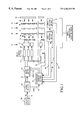
Referring to FIG. 1, a display system 10 includes an array 12 of light emitters 14 and an integral array 16 of microlenses 18 according to an embodiment of this invention. There is a one to one correspondence between the light emitter array 12 and the microlens array 16. The array 12 of light emitters 14 may be formed in a variety of manners. For example, the array may be an array of organic light emitting diodes, an array of discrete laser or light emitting diodes, an matrix addressible array, such as a field emission display, or an output of an optical fiber bundle driven by modulated light sources. The microlens array is an an integral refractive microlens array formed of fused silica lenses, such as those available from Mems Optical, Inc. of Huntsville, Ala.
An image source 30 generates an image signal 32 that defines image content and display synchronization. The image signal 32 may be an RGB signal, NTSC signal, VGA signal, SVGA signal, or other formatted color or monochrome video or image data signal. The image signal 32 typically is time allocated into sequential image frames. Each frame is displayed within a requisite time period. Frame rates of 60 Hz and 72 Hz are common for enabling a human eye to perceive a nonflickering image. A signal decoder 34 receives the image signal 32 and extracts image data 36 and image synchronization information 38. Typically, the data 36 is a series of image pixel defining values. For a color display, the data for one pixel set may define the red green and blue pixel components. For purposes herein, a pixel may a color component pixel (e.g., a red pixel, a green pixel, or a blue pixel or a combined pixel formed from red, green and/or blue components). The synchronization information 38 is extracted to define scanning synchronization signals for controlling the timing/addressing of when a given data item within the data stream 36 is to be displayed. The data 36 is stored in an image buffer 40. The synchronization information 38 is processed by an address control processor 42. The image data is output from the image buffer 40 into appropriate image portion buffers 44 under the control of the processor 42.
A respective, serial stream of data 46 is output from each image portion buffer 44 to define the optical state of a corresponding output beam 50. In one embodiment, each serial stream of data 46 is output to a corresponding driver 52 of a light emitter 14. The binary data define the optical output level of the corresponding light emitter 14, according to known digital-to-analog conversion techniques. In an alternative embodiment each light emitter is maintained in an on state, but its output beam is blocked or passed for a period determined by the binary data. Each set of data received in sequence corresponds to an optical state for a pixel defined by the output beam 50.
In a preferred embodiment, the serial streams of data 46 are synchronously fed from each image portion buffer 44 to the respective light emitter drivers 52. Thus, at any given time there is a light beam 50 (e.g., in an optical state corresponding to the data) output from each light emitter 14, and in turn there is a pixel imaged for each light emitter 14. Each light beam 50 is received at a corresponding microlens 18. For each light emitter 14—microlens 18 pair, there also is a corresponding image portion buffer 44, a serial data stream 46, a driver 52 and a light beam 50. Each set of a corresponding light emitter 14, microlens 18, image portion buffer 44, serial data stream 46, driver 52 and light beam 50 form an optical channel 20. Thus, each image portion buffer 44 feeds a serial stream 46 of image data to a driver 52 which modulates a respective light emitter 14 to output a respective light beam 50 toward a respective microlens 18. The microlens 18 receives and passes the light beam 50 toward a display field 22 to define an image pixel.
As the optical channel 20 outputs the beam 50, a mechanical positioner 60 moves the microlens array 16 relative to the light emitter array 12 synchronously with the serial image data streams 46. More specifically, the positioner 60 moves the microlens array 16 relative to the light emitter array 12 to concurrently scan the respective light beams 50. Each optical channel 22 thus defines an image portion within the display field 22. For example, a 500 optical channel display system may have up to 500 image portions concurrently scanned. If the array 12 moves to 700 discrete positions during an image frame, each image portion will have 700 discrete pixels. Such a system would produce 35,000 pixels (500×700) during each frame. One skilled in the art will recognize that the geometry of the image will depend upon the layout of the arrays 12, 16 and the geometry of the scanning pattern.
In one embodiment, the positioner 60 moves the array 16 or the array 12 to scan the light beams 50 along a single scanning axis. In another embodiment, the positioner 60 produces scanning along two scanning axes by moving the microlens array 16 or the light emitter array 12 along each scanning axis.. In the preferred embodiment, the positioner 60 scans the light beams 50 by moving the microlens array 16 relative to the light emitter array 12. However, in alternative embodiments, the light emitter array 12 may be moved instead. In other embodiment, another integral array 19 of microlenses 21 is included. There is a one to one correspondence between the microlenses 21 and the microlenses 18. Thus, each optical channel 20 includes one of the microlenses 21 in addition to the previously described components. A positioner 60 scans the light beams 50 along one axis by moving the microlens array 16 relative to the light emitter array 12. Another positioner 61 scans the light beams 50 along a second axis by moving the microlens array 21 relative to the light emitter array 12 and the first microlens array 16. Accordingly, each light beam 50 is scanned along either one axis or two axes to define a corresponding group of pixels within each respective image portion.
In some embodiments there is still another positioner 58 which repositions the light emitter array 12 and microlens array(s) 16/21 to provide another division of the image frame. The positioner 58 moves the arrays 12, 16 to divide the display field 22 into image subsections 62 (see FIG. 3), while the positioner 60 moves the array 16 relative to the array 12 to divide each subsection 62 into image portions 64.
For a retinal scanning display embodiment, another array 23 of lenses 25 is positioned between the microlens array 16 and the display field 22. Such other array 23 serves as an eyelens.
The light emitter array 12 is formed by a plurality of point or collimated beam sources which generate respective light beams 50. Each light beam 50 may be a coherent or non-coherent beam of light. Preferably, each beam is emitted along an optical axis parallel to those of the other beams of light. In one embodiment each emitter 14 is at a fixed position relative to each other emitter in the array 12. The emitters 14 are formed in various embodiments by light emitting diodes, organic light emitters or lasers.
Image Divisions and Pixel Scanning
Referring to FIG. 2, the display field 22 encompasses an area for projecting an image. Such display field 22 is projected onto a screen or onto a retina of a viewer's eye. An image 23 is presented within the display field 22 by scanning the multiple light beams 50 along prescribed scan paths. The image 23 is formed by one or more image subsections 62. Each image subsection 62 is, in turn, formed by a plurality of image portions 64 and each image portion 64 is formed by a plurality of image pixels 66. FIG. 2 shows a display field 22 with one image subsection 62. FIG. 3 shows a display field 22 with multiple image subsections 62. As can be seen in FIG. 3, each image subsection 62 can include a plurality of image portions 64, which in turn are formed of a plurality of pixels 66. In the preferred embodiment, each image portion 64 includes the same number of image pixels 66.
The image portions 64 may be allocated from the image subsection 62 into a two dimensional array of image portions 64 as shown in FIGS. 2 and 3, or into a one dimensional array of image portions 64 as shown in FIGS. 4 and 5. FIG. 4 shows an array of vertical image portions 64. FIG. 5 shows an array of horizontal image portions 64. Each image portion 64 of FIG. 4 includes the same number and arrangement of image pixels 66 as the other image portions of FIG. 4. Similarly, each image portion 64 of FIG. 5 includes the same number and arrangement of image pixels 66 as the other image portions 64 of FIG. 5. One skilled in the art will recognize that a wide range of combinations of image portions 62 can be used to fill all or a part of the display field 22.
Referring again to FIG. 2, there are 108 image portions 64 depicted. Such number of course may vary. Each image portion 64 corresponds to one of the optical channels 20. Thus, at any given time during an image frame, one pixel is being displayed from each of the image portions 64. The relative position of such one pixel within each image portion 64 is typically the same. Further, because the position of each microlens 18 is fixed relative to the other microlenses in the microlens array 18, and because the position of each light emitter 14 is fixed relative to the other light emitters within the light emitter array 12, the relative scan path within any given image portion 64 is the same. FIG. 2, for example, depicts an array of image portions 64. Each image portion is formed by multiple rows and columns of pixels 66. As will be described below with reference to FIGS. 6a-c, each optical channel 20 scans one horizontal line of pixels 66, then moves down vertically to scan another horizontal line of pixels. This continues until all pixels within the image portion are scanned. Accordingly, two dimensional scanning is performed. Even though the array of image portions in FIG. 2 is two dimensional, two dimensional scanning also may be performed for a one dimensional array of image portions. For such an array each image portion would be formed by a two dimensional array of image pixels.
Referring now to FIG. 6a, an initial position is shown for imaging a first pixel 66 in each image portion 64. A respective light beam 50 is output from each light emitter 14 toward a corresponding microlens 18. The light beam 50 passes through the microlens toward the display field 22 in the current image subsection 62 being scanned. A pixel 66 in each image portion 64 of the image subsection 62 is concurrently scanned. FIG. 6b shows the relative position of the microlens array 18 relative to the light emitter array 12 a short time later when an adjacent pixel is being imaged in each image portion. Note that the microlens array has moved along a first axis x by an increment Dx to position the output beams 50 at the adjacent pixel area within each image portion 64. FIG. 6c shows the relative position of the microlens array 18 relative to the light emitter array 12 at a later time in the image portion scan cycle when another row of pixels is to be imaged. Note that the microlens array has moved along a second axis y by an increment Dy to position the output beams 50 at the adjacent row within each image portion 64.
According to an alternative scanning methodology, each image portion includes a one dimensional array of pixels. One dimensional scanning is performed for such image portions. FIG. 4 depicts a one dimensional array of vertically-oriented image portions 64. Each image portion 64 is formed by one column of image pixels 66. For an exemplary embodiment having 500 optical channels, there are 500 vertical image portions 64. Each optical channel scans vertically to image each pixel 66 within the corresponding column 64 i. FIG. 5 depicts a one-dimensional array of horizontal image portions. Each image portion 64 is formed by one row of image pixels 66. For an exemplary embodiment having 500 optical channels, there are 500 horizontal image portions 64. Each optical channel scans horizontally to image each pixel 66 within the corresponding row 64 i.
FIG. 3 shows an image area 22 formed of multiple subsections 62 a-62 d. The number of subsections may vary. For each subsection 62 i, is formed from a plurality of image portions 64. As described with regard to FIG. 2, each image portion 64 is formed in turn of a two dimensional array of pixels. Alternatively, like in FIG. 4 or FIG. 5 each image portion may be formed of a one dimensional array of image pixels 66. For a two dimensional array of pixels, each image portion 64 is scanned along two axes. For a one dimensional array of pixels, each image portion is scanned along one axis. Once all image portions 64 within a given image subsection 62 i are scanned, the image portions within another image subsection are scanned. The image subsections 62 are scanned in series using one set of optical channels 20 or in parallel using multiple sets of optical channels, wherein each set of optical channels includes an integral microlens array.
Position Drivers
Referring to FIGS. 7a and 7 b, the position driver 60 includes a base 82, a frame 84 and at least one drive circuit 86. For one axis scanning one drive circuit 86 is included. FIG. 8 shows an embodiment of the driver 60′ having two drive circuits 86, 88—one for scanning along each of two axes. The position drive 60 receives a synchronization signal 94 from the processor 42 to synchronize the scanning of the light beams 50. The position driver 60′ receives a pair of synchronization signals 94, 95 from the processor 42. One synchronization signal 94 is for controlling scanning along one axis x, while the other synchronization signal 95 is for controlling scanning along another axis y. Each drive circuit 86, 88 includes a pair of permanent magnets 92, 93 and a pair of electromagnetic coils 96, 98.
The microlens array 16 is mounted to the frame 84 of positioner 60. The frame 84 includes at least two opposing legs 102, 104 protruding from the base 82. The light emitter array 12 is mounted to the base 82. Adjacent to each leg are the permanent magnets 92/94 and the electromagnetic coils 96/98. The synchronization signal 94 is received to energize the coils 96, 98 and generate an alternating magnetic field which deflects the legs 102, 104. The synchronization signal 94 is a periodic signal which drives the coils to induce a magnetic field which moves the legs and thus the microlens array 16 back and forth along a first scanning axis x between a first extreme deflection position and a second extreme deflection position. As a result, the light beams 50 are scanned back and forth along the scanning axis to scan respective lines of pixels 66 within corresponding image portions 64.
For the two-axis driver 60′ of FIG. 8 the frame 84 includes at least four opposing legs 102, 104, 102′, 104′ protruding from the base 82. The light emitter array 12 is mounted to the base 82. Adjacent to each leg is a permanent magnet 92/94, 92′/94′ and an electromagnetic coil 96/98, 96′/98′. A first synchronization signal 94 is received to energize the coils 96, 98 and generate an alternating magnetic field which deflects the legs 102, 104. The synchronization signal 94 is a periodic signal which drives the coils 102, 104 to induce a magnetic field which moves the legs and thus the microlens array 16 back and forth along a first scanning axis x between a first extreme deflection position and a second extreme deflection position. The second synchronization signal 95 is received to energize the coils 96′, 98′ and generate an alternating magnetic field which deflects the legs 102′, 104′. The synchronization signal 95 is a periodic signal which drives the coils 96′, 98′ to induce a magnetic field which moves the legs 102′, 104′ and thus the microlens array 16 back and forth along a second scanning axis y between a first extreme deflection position and a second extreme deflection position. Note that the first scanning axis x is orthogonal to the second scanning axis y. Thus, the legs 102, 104 are positioned orthogonally to the legs 102′, 104′. As a result, the light beams 50 are scanned back and forth along the first scanning axis x and back and forth along the second scanning axis y to scan multiple lines of pixels 66 within corresponding image portions 64.
Piezoelectric sensors 106 are mounted to each leg 102, 104, 102′, 104′ to detect the position of the microlens array 16 relative to the light emitter array 14. The respective sensor output signals 108, 110 are fed back to the processor 42. In one embodiment, the scanning frequency for scanning along the first axis equals the natural resonant frequency of the moving components of driver 60.
FIGS. 9a-9 b show an embodiment of position driver 60 and position driver 61 operating to scan an image portion 64 along two axes x,y. Position driver 60 scans along one axis x and position driver 61 scans along another axis y. Position driver 60 is formed in the manner described above with respect to FIG. 7. Its deflection path is shown in FIG. 9a. Position driver 61 includes similar components and shares a common base 82 with position driver 60. Its deflection path is shown in FIG. 9b. Referring to FIG. 9b, position driver 61 includes a frame 114 having at least two opposing legs 122, 124 protruding from the base 82. The light emitter array 12 is mounted to the base 82. Adjacent to each leg is a permanent magnet 126/128 and an electromagnetic coil 130/132. The synchronization signal 95 is received to energize the coils 130/132 and generate an alternating magnetic field which deflects the legs 122, 124. The synchronization signal 95 is a periodic signal which drives the coils 130/132 to induce a magnetic field which moves the legs 122, 124 and thus the microlens array 19 back and forth along the second scanning axis y between a first extreme deflection position and a second extreme deflection position. Piezoelectric sensors 106 are mounted to the legs 122, 124 to detect the position of the microlens array 19 relative to the base 82. The piezoelectric sensor output signal 110 is fed back to the processor 42. In a preferred two-axis scanning embodiment, the scanning frequency for scanning along the first axis equals the natural resonant frequency of the moving components of driver 60, and the scanning frequency for scanning along the second axis equals the natural resonant frequency of the moving components of driver 61.
FIG. 10 shows an alternative embodiment 160 to the one-axis position driver 60 of FIGS. 7a-7 b having a piezoelectric actuator instead of an electromagnetic drive circuit. Each leg 102, 104 includes at least one piezoelectric volume 120 which receives the synchronization signal 94. The synchronization signal is a periodic signal which causes the piezoelectric volumes to deform. Such deformation deflects the legs 102, 104 back and forth along the scanning axis x.
FIGS. 10-11 show an alternative embodiment 160′ to the two-axis position driver 60′ of FIG. 8 having a pair of piezoelectric actuators instead of a pair of electromagnetic drive circuits. FIG. 10 shows the two axis position driver 160′ in a view depicting scanning along one axis x. FIG. 11 depicts the driver 160′ scanning along the other axis y. Each leg 102, 104, 102′, 104′ includes at least one piezoelectric volume 120. Legs 102, 104 receive the synchronization signal 94. Legs 102′, 104′ receive the synchronization signal 95. The synchronization signals 94, 95 are periodic signals which cause the piezoelectric volumes 120 to deform. Such deformation deflects the legs 102, 104 back and forth along the scanning axis x, and the legs 102′, 104′ back and forth along the scanning axis y. Note that the legs 102, 104 are coupled to the base 82 in a manner allowing the legs 102, 104 free movement along the y axis. The legs 102, 104 are fixed relative to the x axis, but deform to scan the microlens array 16 along such x axis. Similarly, the legs 102′, 104′ are coupled to the base 82 in a manner allowing the legs 102′, 104′ free movement along the x axis. The legs 102′, 104′ are fixed relative to the y axis, but deform to scan the microlens array 16 along such y axis.
FIGS. 12a-12 b show an alternative embodiment to the stacked position drivers 60, 61 of FIG. 9 having piezoelectric actuators instead of electromagnetic drive circuits. Each leg 102, 104, 122, 124 includes at least one piezoelectric volume 120. Legs 102, 104 receive the synchronization signal 94. Legs 122, 124 receive the synchronization signal 95. The synchronization signals 94, 95 are periodic signals which cause the piezoelectric volumes 120 to deform. Such deformation deflects the legs 102, 104 back and forth along the scanning axis x, and the legs 122, 124 back and forth along the scanning axis y.
Although a preferred embodiment of the invention has been illustrated and described, various alternatives, modifications and equivalents may be used. Therefore, the foregoing description should not be taken as limiting the scope of the inventions which are defined by the appended claims.

Claims (24)

What is claimed is:
1. A display apparatus for presenting an image, the image including at least one image section made up of a plurality of image portions, each one of the plurality of image portions including a plurality of image pixels, the apparatus comprising:
a plurality of light emitters, each one light emitter being operative to emit a beam of light in response to an input signal;
a microlens array including a plurality of microlenses, each one microlens of the plurality of microlenses corresponding to a respective one light emitter of the plurality of light emitters to receive a corresponding beam of light from said corresponding one light emitter, wherein the microlens array passes a plurality of beams of light, each one of the plurality of passed beams of light corresponding to one microlens, one light emitter and one emitted beam of light,
wherein each one microlens of the plurality of microlenses, the corresponding one light emitter and the corresponding emitted, received and passed beam of light together correspond to one image portion of the plurality of image portions within said one image section, the microlens array being movable through a plurality of positions relative to the plurality of light emitters to scan each one of said plurality of passed beams of light to each image pixel of the plurality of image pixels within the corresponding image portion; and
a positioner which moves the microlens array relative to the plurality of light emitters in a predetermined pattern in which each one microlens scans the corresponding passed beam of light to each image pixel of the corresponding image portion.
2. A display apparatus for presenting an image, the image including at least one image section made up of a plurality of image portions, each one of the plurality of image portions including a plurality of image pixels, the apparatus comprising:
a plurality of light emitters, each one light emitter being operative to emit a beam of light in response to an input signal;
a microlens array including a plurality of microlenses, each one microlens of the plurality of microlenses corresponding to a respective one light emitter of the plurality of light emitters to receive a corresponding beam of light from said corresponding one light emitter, wherein the microlens array passes a plurality of beams of light, each one of the plurality of passed beams of light corresponding to one microlens, one light emitter and one emitted beam of light,
wherein each one microlens of the plurality of microlenses, the corresponding one light emitter and the corresponding emitted, received and passed beam of light together correspond to one image portion of the plurality of image portions within said one image section, the microlens array being movable through a plurality of positions relative to the plurality of light emitters to scan each one of said plurality of passed beams of light to each image pixel of the plurality of image pixels within the corresponding image portion; and
a first positioner which moves the microlens array relative to the plurality of light emitters in a predetermined pattern in which each one microlens scans the corresponding passed beam of light to each image pixel of the corresponding image portion;
in which the image includes a plurality of image sections, each one image section of the plurality of image sections comprising a plurality of image portions, and a second positioner which relocates the plurality of light emitters, the microlens array and the first positioner to scan the plurality of image portions of another image section of the plurality of image sections.
3. The display apparatus of claim 1, in which the plurality of light emitters are aligned in a one-dimensional array of light emitters along a first axis, in which the microlens array is a one dimensional array of microlenses aligned along a second axis parallel to the first axis, and in which the plurality of image pixels in said one image portion corresponding to said one light emitter and said one microlens are aligned along a third axis orthogonal to said first axis and said second axis.
4. The display apparatus of claim 1, in which the plurality of light emitters are aligned in a two-dimensional array of light emitters, in which the microlens array is a two dimensional array of microlenses, and in which the plurality of image pixels in said one image portion corresponding to said one light emitter and said one microlens are arranged in a two dimensional array of image pixels.
5. The display apparatus of claim 1, in which the positioner comprises an electromagnetic drive circuit.
6. The display apparatus of claim 1, in which the positioner comprises a piezoelectric drive actuator.
7. The display apparatus of claim 1, in which each one of the plurality of light emitters is directly modulated to define image content.
8. The display apparatus of claim 1, in which each one of the plurality of light emitters is a light emitting diode.
9. The display apparatus of claim 1, in which each one of the plurality of light emitters is an organic light emitter.
10. The display apparatus of claim 1, further comprising an image screen upon which the plurality of passed beams of light are projected to present the image.
11. The display apparatus of claim 1, further comprising an eyepiece through which the plurality of passed beams of light pass to present the image upon a viewer's retina.
12. An apparatus for displaying an image in response to an image signal, the image including at least one image section, said at least one image section including an array of image portions, the apparatus comprising:
an array of modulatable light sources, each one light source of the array of light sources being responsive to a respective drive signal to provide a modulated light beam corresponding to the drive signal;
an integral array of microlenses, each one microlens of the array of microlenses being positioned to receive a modulated light beam from a corresponding one light source; a mechanical positioner coupled to the array of microlenses, the positioner being responsive to a periodic scan signal to move the array through a periodic scan pattern substantially transverse to the modulated light beams; and
an electronic controller electrically coupled to the array of modulatable light sources that provides the respective drive signals in response to the image signal, the electronic controller further being electrically coupled to the mechanical positioner and operative to produce the periodic scan signal.
13. The display apparatus of claim 12, in which the positioner comprises an electromagnetic drive circuit.
14. The display apparatus of claim 12, in which the positioner comprises a piezoelectric drive actuator.
15. The display apparatus of claim 12, in which each one of the plurality of light emitters is directly modulated to define image content.
16. The display apparatus of claim 12, in which each one of the plurality of light emitters is a light emitting diode.
17. The display apparatus of claim 12, in which each one of the plurality of light emitters is an organic light emitter.
18. The display apparatus of claim 12, wherein the electronic controller includes:
a central processor; and
an electronic memory coupled to the central processor and structured to store data from the image signal.
19. The apparatus of claim 18, wherein the memory is segmented into blocks, each block corresponding to a respective image portion, and wherein the electronic controller further includes an address decoder operative to direct data from the image signal to respective memory blocks.
20. A method of displaying an image, comprising the steps of:
emitting respective first beams of light from a plurality of first locations at a first time;
receiving the first beams to a first set of beam locations within a microlens array;
emitting respective second beams of light from the plurality of first locations at a second time after said first time;
directing the second beams to a second set of beam locations within the microlens array by moving all of the microlenses simultaneously relative to the plurality of first locations.
21. A method for scanning an image, the image including a plurality of image portions, each one image portion of the plurality of image portions including a plurality of image pixels, the method comprising the steps of:
emitting a plurality of beams of light from a plurality of first locations, wherein the plurality of first locations are arranged in a first array;
receiving the plurality of beams of light at an integral array of microlenses, each one microlens passing the received beam of light to generate an image pixel of a corresponding image portion;
moving the microlens array relative to the first array wherein the passed beam of light received at said each one microlens is scanned to generate other image pixels of each corresponding image portion.
22. The method of claim 21, in which the first array is a one dimensional array extending along a first axis, in which the microlens array is a one dimensional array extending along a second axis, and in which the plurality of image pixels in each said one image portion extend along a third axis orthogonal to the first axis and the second axis, and in which the step of moving comprises moving the microlens array relative to the first array along the third axis wherein the passed beam of light received at said each one microlens is scanned to generate said other image pixels of each corresponding image portion.
23. The method of claim 21, in which the first array is a two dimensional array, in which the microlens array is a two dimensional array, and in which the plurality of image pixels in each said one image portion are located within a two dimensional array, and in which the step of moving comprises moving the microlens array relative to the first array along a first scanning axis and a second scanning axis wherein the passed beam of light received at said each one microlens is scanned to generate said other image pixels of each corresponding image portion.
24. A method for scanning an image, the image including a plurality of image portions, each one image portion of the plurality of image portions including a plurality of image pixels, the method comprising the steps of:
emitting a plurality of beams of light from a plurality of first locations, wherein the plurality of first locations are arranged in a first array;
receiving the plurality of beams of light at an integral array of microlenses, each one microlens passing the received beam of light to generate an image pixel of a corresponding image portion;
moving the microlens array relative to the first array wherein the passed beam of light received at said each one microlens is scanned to generate other image pixels of each corresponding image portion, in which the integral array of microlenses is a first microlens array;
receiving the plurality of passed beams of light at an integral second array of microlenses, each one microlens of the second microlens array passing the received beam of light to generate an image pixel of a corresponding image portion; and
moving the second microlens array relative to the first array and first microlens array wherein the passed beam of light received at said each one microlens of the second microlens array is scanned to generate other image pixels of each corresponding image portion;
wherein the step of moving the first microlens array scans the light beams along a first axis to generate image pixels within each corresponding image portion along said first axis, and wherein the step of moving the second microlens array scans the light beams along a second axis to generate image pixels within each corresponding image portion along said second axis.
US09/072,012 1997-05-07 1998-05-04 Image display with lens array scanning relative to light source array Expired - Lifetime US6204832B1 (en)

Priority Applications (1)

Application Number Priority Date Filing Date Title
US09/072,012 US6204832B1 (en) 1997-05-07 1998-05-04 Image display with lens array scanning relative to light source array

Applications Claiming Priority (2)

Application Number Priority Date Filing Date Title
US4583997P 1997-05-07 1997-05-07
US09/072,012 US6204832B1 (en) 1997-05-07 1998-05-04 Image display with lens array scanning relative to light source array

Publications (1)

Publication Number Publication Date
US6204832B1 true US6204832B1 (en) 2001-03-20

Family

ID=26723253

Family Applications (1)

Application Number Title Priority Date Filing Date
US09/072,012 Expired - Lifetime US6204832B1 (en) 1997-05-07 1998-05-04 Image display with lens array scanning relative to light source array

Country Status (1)

Country Link
US (1) US6204832B1 (en)

Cited By (53)

* Cited by examiner, † Cited by third party
Publication number Priority date Publication date Assignee Title
US20020050956A1 (en) * 2000-09-11 2002-05-02 Microvision, Inc. Scanned display with pinch, timing, and distortion correction
US6388641B2 (en) * 1998-11-09 2002-05-14 University Of Washington Scanned beam display with adjustable accommodation
US20020080096A1 (en) * 2000-12-08 2002-06-27 The University Of Tokyo Image displaying method and an image display
US20030058190A1 (en) * 2001-09-21 2003-03-27 Microvision, Inc. Scanned display with pinch, timing, and distortion correction
US6697034B2 (en) * 1999-12-30 2004-02-24 Craig Stuart Tashman Volumetric, stage-type three-dimensional display, capable of producing color images and performing omni-viewpoint simulated hidden line removal
US20050001541A1 (en) * 2000-05-06 2005-01-06 Semiconductor Energy Laboratory Co., Ltd., A Japan Corporation Light-emitting device and electric apparatus
US20050059487A1 (en) * 2003-09-12 2005-03-17 Wilder Richard L. Three-dimensional autostereoscopic image display for a gaming apparatus
DE102004020615A1 (en) * 2004-04-27 2005-11-24 Diehl Bgt Defence Gmbh & Co. Kg Imaging object scene on detector, e.g. for monitoring airspace around aircraft, by oscillating optical element during integration and movement phases at resonant frequency of drive
US20050264502A1 (en) * 2004-05-07 2005-12-01 Sprague Randall B Scanned light display system using large numerical aperture light source, method of using same, and method of making scanning mirror assemblies
US20060017653A1 (en) * 2004-07-26 2006-01-26 Che-Chih Tsao Active screen volumetric 3D display
US20060061846A1 (en) * 2004-09-17 2006-03-23 Microvision, Inc. Scanned light display system using array of collimating elements in conjunction with large numerical aperture light emitter array
US20060284790A1 (en) * 1998-08-05 2006-12-21 Tegreene Clarence T Optical scanning system with correction
US20070060390A1 (en) * 2005-09-13 2007-03-15 Igt Gaming machine with scanning 3-D display system
US20070103449A1 (en) * 2005-11-08 2007-05-10 Nokia Corporation Cost efficient element for combined piezo sensor and actuator in robust and small touch screen realization and method for operation thereof
US20080018641A1 (en) * 2006-03-07 2008-01-24 Sprague Randall B Display configured for varying the apparent depth of selected pixels
US20080043487A1 (en) * 2006-08-21 2008-02-21 Sprague Randall B Light bar structure having light conduits and scanned light display system employing same
US20080073517A1 (en) * 2006-09-13 2008-03-27 Charles David Melville Temperature adjustment in scanning beam devices
US20080106777A1 (en) * 2006-11-03 2008-05-08 Weir Michael P Resonant fourier scanning
US20080144998A1 (en) * 2006-12-15 2008-06-19 University Of Washington Attaching optical fibers to actuator tubes with beads acting as spacers and adhesives
US20080146898A1 (en) * 2006-12-19 2008-06-19 Ethicon Endo-Surgery, Inc. Spectral windows for surgical treatment through intervening fluids
US20080151343A1 (en) * 2006-12-22 2008-06-26 Ethicon Endo-Surgery, Inc. Apparatus including a scanned beam imager having an optical dome
US20080154248A1 (en) * 2006-12-22 2008-06-26 Ethicon Endo-Surgery, Inc. Apparatus and method for medically treating a tattoo
US20080165360A1 (en) * 2007-01-10 2008-07-10 University Of Washington Scanning beam device calibration
US20080167546A1 (en) * 2007-01-09 2008-07-10 Ethicon Endo-Surgery, Inc. Methods for imaging the anatomy with an anatomically secured scanner assembly
US20080173803A1 (en) * 2007-01-18 2008-07-24 Ethicon Endo-Surgery, Inc. Scanning beam imaging with adjustable detector sensitivity or gain
US20080226029A1 (en) * 2007-03-12 2008-09-18 Weir Michael P Medical device including scanned beam unit for imaging and therapy
US20080249369A1 (en) * 2007-04-05 2008-10-09 University Of Washington Compact scanning fiber device
US20080265178A1 (en) * 2007-04-26 2008-10-30 University Of Washington Driving scanning fiber devices with variable frequency drive signals
US20080281159A1 (en) * 2007-05-08 2008-11-13 University Of Washington Coordinating image acquisition among multiple endoscopes
US20080281207A1 (en) * 2007-05-08 2008-11-13 University Of Washington Image acquisition through filtering in multiple endoscope systems
US20080291597A1 (en) * 2007-05-22 2008-11-27 Seibel Eric J Scanning beam device having different image acquisition modes
US20080297537A1 (en) * 2007-05-31 2008-12-04 Motorola, Inc. Devices and methods for synchronized illumination
US20090002794A1 (en) * 2007-06-29 2009-01-01 Ethicon Endo-Surgery, Inc. Receiver aperture broadening for scanned beam imaging
US20090015695A1 (en) * 2007-07-13 2009-01-15 Ethicon Endo-Surgery, Inc. Sbi motion artifact removal apparatus and method
US20090021818A1 (en) * 2007-07-20 2009-01-22 Ethicon Endo-Surgery, Inc. Medical scanning assembly with variable image capture and display
US20090026888A1 (en) * 2007-07-25 2009-01-29 University Of Washington Actuating an optical fiber with a piezoelectric actuator and detecting voltages generated by the piezoelectric actuator
US20090036734A1 (en) * 2007-07-31 2009-02-05 Ethicon Endo-Surgery, Inc. Devices and methods for introducing a scanning beam unit into the anatomy
US20090079941A1 (en) * 2007-09-20 2009-03-26 Microvision, Inc. Three-dimensional image projection system and method
US20090092364A1 (en) * 2007-10-04 2009-04-09 University Of Washington Reducing distortion in scanning fiber devices
US20090103882A1 (en) * 2006-12-15 2009-04-23 Charles David Melville Attaching optical fibers to actuator tubes with beads acting as spacers and adhesives
US20090141997A1 (en) * 2007-11-30 2009-06-04 University Of Washington Reducing noise in images acquired with a scanning beam device
US20090245599A1 (en) * 2008-03-27 2009-10-01 Ethicon Endo-Surgery, Inc. Method for creating a pixel image from sampled data of a scanned beam imager
US20090270724A1 (en) * 2008-04-25 2009-10-29 Ethicon Endo-Surgery, Inc. Scanned beam device and method using same which measures the reflectance of patient tissue
US7925333B2 (en) 2007-08-28 2011-04-12 Ethicon Endo-Surgery, Inc. Medical device including scanned beam unit with operational control features
US7983739B2 (en) 2007-08-27 2011-07-19 Ethicon Endo-Surgery, Inc. Position tracking and control for a scanning assembly
US7995045B2 (en) 2007-04-13 2011-08-09 Ethicon Endo-Surgery, Inc. Combined SBI and conventional image processor
US8160678B2 (en) 2007-06-18 2012-04-17 Ethicon Endo-Surgery, Inc. Methods and devices for repairing damaged or diseased tissue using a scanning beam assembly
US8216214B2 (en) 2007-03-12 2012-07-10 Ethicon Endo-Surgery, Inc. Power modulation of a scanning beam for imaging, therapy, and/or diagnosis
WO2012113856A1 (en) * 2011-02-25 2012-08-30 Trilite Technologies Gmbh Display device with movement elements for obtaining a high resolution and/or a 3d effect
US8626271B2 (en) 2007-04-13 2014-01-07 Ethicon Endo-Surgery, Inc. System and method using fluorescence to examine within a patient's anatomy
US8801606B2 (en) 2007-01-09 2014-08-12 Ethicon Endo-Surgery, Inc. Method of in vivo monitoring using an imaging system including scanned beam imaging unit
US20150156478A1 (en) * 2012-08-06 2015-06-04 Fujifilm Corporation Imaging device
US9079762B2 (en) 2006-09-22 2015-07-14 Ethicon Endo-Surgery, Inc. Micro-electromechanical device

Citations (8)

* Cited by examiner, † Cited by third party
Publication number Priority date Publication date Assignee Title
US5467104A (en) 1992-10-22 1995-11-14 Board Of Regents Of The University Of Washington Virtual retinal display
US5557444A (en) 1994-10-26 1996-09-17 University Of Washington Miniature optical scanner for a two axis scanning system
US5587836A (en) 1993-05-13 1996-12-24 Olympus Optical Co., Ltd. Visual display apparatus
US5596339A (en) 1992-10-22 1997-01-21 University Of Washington Virtual retinal display with fiber optic point source
US5694237A (en) * 1996-09-25 1997-12-02 University Of Washington Position detection of mechanical resonant scanner mirror
US5701132A (en) 1996-03-29 1997-12-23 University Of Washington Virtual retinal display with expanded exit pupil
US5815314A (en) * 1993-12-27 1998-09-29 Canon Kabushiki Kaisha Image display apparatus and image display method
US6008781A (en) * 1992-10-22 1999-12-28 Board Of Regents Of The University Of Washington Virtual retinal display

Patent Citations (9)

* Cited by examiner, † Cited by third party
Publication number Priority date Publication date Assignee Title
US5467104A (en) 1992-10-22 1995-11-14 Board Of Regents Of The University Of Washington Virtual retinal display
US5596339A (en) 1992-10-22 1997-01-21 University Of Washington Virtual retinal display with fiber optic point source
US6008781A (en) * 1992-10-22 1999-12-28 Board Of Regents Of The University Of Washington Virtual retinal display
US5587836A (en) 1993-05-13 1996-12-24 Olympus Optical Co., Ltd. Visual display apparatus
US5815314A (en) * 1993-12-27 1998-09-29 Canon Kabushiki Kaisha Image display apparatus and image display method
US5557444A (en) 1994-10-26 1996-09-17 University Of Washington Miniature optical scanner for a two axis scanning system
US5701132A (en) 1996-03-29 1997-12-23 University Of Washington Virtual retinal display with expanded exit pupil
US5969871A (en) * 1996-03-29 1999-10-19 University Of Washington Virtual retinal display with lens array for expanding exit pupil
US5694237A (en) * 1996-09-25 1997-12-02 University Of Washington Position detection of mechanical resonant scanner mirror

Non-Patent Citations (1)

* Cited by examiner, † Cited by third party
Title
"Refractive Microlens Arrays," MEMS Optical, Inc., Huntsville, Alabama, 1998.

Cited By (93)

* Cited by examiner, † Cited by third party
Publication number Priority date Publication date Assignee Title
US20060284790A1 (en) * 1998-08-05 2006-12-21 Tegreene Clarence T Optical scanning system with correction
US20080136742A1 (en) * 1998-08-05 2008-06-12 Microvision, Inc. Method and Apparatus for Compensating for Distortion in a Scanned Beam System
US7428093B2 (en) 1998-08-05 2008-09-23 Microvision, Inc. Optical scanning system with correction
US6388641B2 (en) * 1998-11-09 2002-05-14 University Of Washington Scanned beam display with adjustable accommodation
US6697034B2 (en) * 1999-12-30 2004-02-24 Craig Stuart Tashman Volumetric, stage-type three-dimensional display, capable of producing color images and performing omni-viewpoint simulated hidden line removal
US20050001541A1 (en) * 2000-05-06 2005-01-06 Semiconductor Energy Laboratory Co., Ltd., A Japan Corporation Light-emitting device and electric apparatus
US7679092B2 (en) * 2000-05-06 2010-03-16 Semiconductor Energy Laboratory Co., Ltd. Light-emitting device having an electroluminescence element
US20020050956A1 (en) * 2000-09-11 2002-05-02 Microvision, Inc. Scanned display with pinch, timing, and distortion correction
US20020080096A1 (en) * 2000-12-08 2002-06-27 The University Of Tokyo Image displaying method and an image display
US6806851B2 (en) * 2000-12-08 2004-10-19 The University Of Tokyo Image displaying method and an image display
US7023402B2 (en) * 2001-09-21 2006-04-04 Microvision, Inc. Scanned display with pinch, timing, and distortion correction
US20030058190A1 (en) * 2001-09-21 2003-03-27 Microvision, Inc. Scanned display with pinch, timing, and distortion correction
US7857700B2 (en) 2003-09-12 2010-12-28 Igt Three-dimensional autostereoscopic image display for a gaming apparatus
US20050059487A1 (en) * 2003-09-12 2005-03-17 Wilder Richard L. Three-dimensional autostereoscopic image display for a gaming apparatus
DE102004020615B4 (en) * 2004-04-27 2007-02-22 Diehl Bgt Defence Gmbh & Co. Kg Method and device for imaging an object scene onto a detector
DE102004020615A1 (en) * 2004-04-27 2005-11-24 Diehl Bgt Defence Gmbh & Co. Kg Imaging object scene on detector, e.g. for monitoring airspace around aircraft, by oscillating optical element during integration and movement phases at resonant frequency of drive
US7724210B2 (en) 2004-05-07 2010-05-25 Microvision, Inc. Scanned light display system using large numerical aperture light source, method of using same, and method of making scanning mirror assemblies
US20050264502A1 (en) * 2004-05-07 2005-12-01 Sprague Randall B Scanned light display system using large numerical aperture light source, method of using same, and method of making scanning mirror assemblies
US7639209B2 (en) 2004-05-07 2009-12-29 Microvision, Inc. Scanned light display system using large numerical aperture light source, method of using same, and method of making scanning mirror assemblies
US20060181484A1 (en) * 2004-05-07 2006-08-17 Sprague Randall B Scanned light display system using large numerical aperture light source, method of using same, and method of making scanning mirror assemblies
US20060017653A1 (en) * 2004-07-26 2006-01-26 Che-Chih Tsao Active screen volumetric 3D display
US8022895B2 (en) * 2004-07-26 2011-09-20 Che-Chih Tsao Active screen volumetric 3D display
US20060061846A1 (en) * 2004-09-17 2006-03-23 Microvision, Inc. Scanned light display system using array of collimating elements in conjunction with large numerical aperture light emitter array
US20060187512A1 (en) * 2004-09-17 2006-08-24 Sprague Randall B Scanned light display system using array of collimating elements in conjunction with large numerical aperture light emitter array
US7365892B2 (en) 2004-09-17 2008-04-29 Microvision, Inc. Scanned light display system using array of collimating elements in conjunction with large numerical aperture light emitter array
US7878910B2 (en) * 2005-09-13 2011-02-01 Igt Gaming machine with scanning 3-D display system
US20070060390A1 (en) * 2005-09-13 2007-03-15 Igt Gaming machine with scanning 3-D display system
US9001045B2 (en) * 2005-11-08 2015-04-07 Nokia Corporation Cost efficient element for combined piezo sensor and actuator in robust and small touch screen realization and method for operation thereof
US20070103449A1 (en) * 2005-11-08 2007-05-10 Nokia Corporation Cost efficient element for combined piezo sensor and actuator in robust and small touch screen realization and method for operation thereof
US20080018641A1 (en) * 2006-03-07 2008-01-24 Sprague Randall B Display configured for varying the apparent depth of selected pixels
US20080043487A1 (en) * 2006-08-21 2008-02-21 Sprague Randall B Light bar structure having light conduits and scanned light display system employing same
US20080073517A1 (en) * 2006-09-13 2008-03-27 Charles David Melville Temperature adjustment in scanning beam devices
US7680373B2 (en) 2006-09-13 2010-03-16 University Of Washington Temperature adjustment in scanning beam devices
US9079762B2 (en) 2006-09-22 2015-07-14 Ethicon Endo-Surgery, Inc. Micro-electromechanical device
US20080106777A1 (en) * 2006-11-03 2008-05-08 Weir Michael P Resonant fourier scanning
US7738762B2 (en) 2006-12-15 2010-06-15 University Of Washington Attaching optical fibers to actuator tubes with beads acting as spacers and adhesives
US7447415B2 (en) 2006-12-15 2008-11-04 University Of Washington Attaching optical fibers to actuator tubes with beads acting as spacers and adhesives
US20080144998A1 (en) * 2006-12-15 2008-06-19 University Of Washington Attaching optical fibers to actuator tubes with beads acting as spacers and adhesives
US20090103882A1 (en) * 2006-12-15 2009-04-23 Charles David Melville Attaching optical fibers to actuator tubes with beads acting as spacers and adhesives
US20080146898A1 (en) * 2006-12-19 2008-06-19 Ethicon Endo-Surgery, Inc. Spectral windows for surgical treatment through intervening fluids
US7713265B2 (en) 2006-12-22 2010-05-11 Ethicon Endo-Surgery, Inc. Apparatus and method for medically treating a tattoo
US20080154248A1 (en) * 2006-12-22 2008-06-26 Ethicon Endo-Surgery, Inc. Apparatus and method for medically treating a tattoo
US20080151343A1 (en) * 2006-12-22 2008-06-26 Ethicon Endo-Surgery, Inc. Apparatus including a scanned beam imager having an optical dome
US8273015B2 (en) 2007-01-09 2012-09-25 Ethicon Endo-Surgery, Inc. Methods for imaging the anatomy with an anatomically secured scanner assembly
US8801606B2 (en) 2007-01-09 2014-08-12 Ethicon Endo-Surgery, Inc. Method of in vivo monitoring using an imaging system including scanned beam imaging unit
US20080167546A1 (en) * 2007-01-09 2008-07-10 Ethicon Endo-Surgery, Inc. Methods for imaging the anatomy with an anatomically secured scanner assembly
US9066651B2 (en) 2007-01-10 2015-06-30 University Of Washington Scanning beam device calibration
US20080165360A1 (en) * 2007-01-10 2008-07-10 University Of Washington Scanning beam device calibration
US8305432B2 (en) 2007-01-10 2012-11-06 University Of Washington Scanning beam device calibration
US9639934B2 (en) 2007-01-10 2017-05-02 University Of Washington Scanning beam device calibration
US20080173803A1 (en) * 2007-01-18 2008-07-24 Ethicon Endo-Surgery, Inc. Scanning beam imaging with adjustable detector sensitivity or gain
US8216214B2 (en) 2007-03-12 2012-07-10 Ethicon Endo-Surgery, Inc. Power modulation of a scanning beam for imaging, therapy, and/or diagnosis
US20080226029A1 (en) * 2007-03-12 2008-09-18 Weir Michael P Medical device including scanned beam unit for imaging and therapy
US20080249369A1 (en) * 2007-04-05 2008-10-09 University Of Washington Compact scanning fiber device
US7583872B2 (en) 2007-04-05 2009-09-01 University Of Washington Compact scanning fiber device
US7995045B2 (en) 2007-04-13 2011-08-09 Ethicon Endo-Surgery, Inc. Combined SBI and conventional image processor
US8626271B2 (en) 2007-04-13 2014-01-07 Ethicon Endo-Surgery, Inc. System and method using fluorescence to examine within a patient's anatomy
US20080265178A1 (en) * 2007-04-26 2008-10-30 University Of Washington Driving scanning fiber devices with variable frequency drive signals
US7608842B2 (en) 2007-04-26 2009-10-27 University Of Washington Driving scanning fiber devices with variable frequency drive signals
US20080281207A1 (en) * 2007-05-08 2008-11-13 University Of Washington Image acquisition through filtering in multiple endoscope systems
US20080281159A1 (en) * 2007-05-08 2008-11-13 University Of Washington Coordinating image acquisition among multiple endoscopes
US20080291597A1 (en) * 2007-05-22 2008-11-27 Seibel Eric J Scanning beam device having different image acquisition modes
US8212884B2 (en) 2007-05-22 2012-07-03 University Of Washington Scanning beam device having different image acquisition modes
US20080297537A1 (en) * 2007-05-31 2008-12-04 Motorola, Inc. Devices and methods for synchronized illumination
US8049689B2 (en) * 2007-05-31 2011-11-01 Motorola Mobility, Inc. Devices and methods for synchronized illumination
US8160678B2 (en) 2007-06-18 2012-04-17 Ethicon Endo-Surgery, Inc. Methods and devices for repairing damaged or diseased tissue using a scanning beam assembly
US20090002794A1 (en) * 2007-06-29 2009-01-01 Ethicon Endo-Surgery, Inc. Receiver aperture broadening for scanned beam imaging
US7982776B2 (en) 2007-07-13 2011-07-19 Ethicon Endo-Surgery, Inc. SBI motion artifact removal apparatus and method
US20090015695A1 (en) * 2007-07-13 2009-01-15 Ethicon Endo-Surgery, Inc. Sbi motion artifact removal apparatus and method
US20090021818A1 (en) * 2007-07-20 2009-01-22 Ethicon Endo-Surgery, Inc. Medical scanning assembly with variable image capture and display
US8437587B2 (en) 2007-07-25 2013-05-07 University Of Washington Actuating an optical fiber with a piezoelectric actuator and detecting voltages generated by the piezoelectric actuator
US20090026888A1 (en) * 2007-07-25 2009-01-29 University Of Washington Actuating an optical fiber with a piezoelectric actuator and detecting voltages generated by the piezoelectric actuator
US20090036734A1 (en) * 2007-07-31 2009-02-05 Ethicon Endo-Surgery, Inc. Devices and methods for introducing a scanning beam unit into the anatomy
US9125552B2 (en) 2007-07-31 2015-09-08 Ethicon Endo-Surgery, Inc. Optical scanning module and means for attaching the module to medical instruments for introducing the module into the anatomy
US7983739B2 (en) 2007-08-27 2011-07-19 Ethicon Endo-Surgery, Inc. Position tracking and control for a scanning assembly
US7925333B2 (en) 2007-08-28 2011-04-12 Ethicon Endo-Surgery, Inc. Medical device including scanned beam unit with operational control features
US20090079941A1 (en) * 2007-09-20 2009-03-26 Microvision, Inc. Three-dimensional image projection system and method
US7522813B1 (en) 2007-10-04 2009-04-21 University Of Washington Reducing distortion in scanning fiber devices
US20090092364A1 (en) * 2007-10-04 2009-04-09 University Of Washington Reducing distortion in scanning fiber devices
US8411922B2 (en) 2007-11-30 2013-04-02 University Of Washington Reducing noise in images acquired with a scanning beam device
US20090141997A1 (en) * 2007-11-30 2009-06-04 University Of Washington Reducing noise in images acquired with a scanning beam device
US8050520B2 (en) 2008-03-27 2011-11-01 Ethicon Endo-Surgery, Inc. Method for creating a pixel image from sampled data of a scanned beam imager
US20090245599A1 (en) * 2008-03-27 2009-10-01 Ethicon Endo-Surgery, Inc. Method for creating a pixel image from sampled data of a scanned beam imager
US20090270724A1 (en) * 2008-04-25 2009-10-29 Ethicon Endo-Surgery, Inc. Scanned beam device and method using same which measures the reflectance of patient tissue
US8332014B2 (en) 2008-04-25 2012-12-11 Ethicon Endo-Surgery, Inc. Scanned beam device and method using same which measures the reflectance of patient tissue
WO2012113883A3 (en) * 2011-02-25 2012-11-01 Trilite Technologies Gmbh Illumination device with movement elements
WO2012113856A1 (en) * 2011-02-25 2012-08-30 Trilite Technologies Gmbh Display device with movement elements for obtaining a high resolution and/or a 3d effect
CN103534745A (en) * 2011-02-25 2014-01-22 特里利特技术有限公司 Display device with movement elements for obtaining a high resolution and/or a 3D effect
US9121574B2 (en) 2011-02-25 2015-09-01 Trilite Technologies Gmbh Illumination device with movement elements
US9689551B2 (en) 2011-02-25 2017-06-27 Trilite Technologies Gmbh Display device with movement elements for obtaining a high resolution and/or a 3D effect
CN103534745B (en) * 2011-02-25 2017-08-22 特里利特技术有限公司 Display device with the moving element for obtaining high-resolution and/or 3D effect
US20150156478A1 (en) * 2012-08-06 2015-06-04 Fujifilm Corporation Imaging device
US9723292B2 (en) * 2012-08-06 2017-08-01 Fujifilm Corporation Imaging device

Similar Documents

Publication Publication Date Title
US6204832B1 (en) Image display with lens array scanning relative to light source array
EP1006857B1 (en) Point source scanning apparatus and method
US10896491B2 (en) Device and method for projecting an image
US5091719A (en) Helmet display
CA2220283C (en) Virtual retinal display with fiber optic point source
US4897715A (en) Helmet display
JP4561794B2 (en) Aerial image display device
US6839042B2 (en) Light beam display with interlaced light beam scanning
US10951867B2 (en) Light emitter architecture for scanning display device
JP4006179B2 (en) Image display device and image display system
US7023402B2 (en) Scanned display with pinch, timing, and distortion correction
JPH07506220A (en) Vertical cavity/surface emitting laser array display system
US20110122236A1 (en) Spatial image display apparatus
EP0547493A1 (en) Virtual display device and method of use
JP2022531073A (en) Reduction of peak current usage in light emitting diode arrays
US10114215B1 (en) Scanning laser devices with reduced exit pupil disparity
JP2019534467A (en) Apparatus and method for providing depth mapping along with scanning of laser image projection
CN108702495B (en) Multi-stripe laser for laser-based projector displays
US6860606B2 (en) Projector having concentrated beam
CN114488539A (en) Scanning display module and near-to-eye display equipment
US11290694B1 (en) Image projector with high dynamic range
JP5041258B2 (en) Aerial image display device
JPH04181289A (en) Picture display device
EP1655629A2 (en) Point source scanning apparatus and method
KR100275387B1 (en) Virtual reality display

Legal Events

Date Code Title Description
AS Assignment

Owner name: WASHINGTON, UNIVERSITY OF, WASHINGTON

Free format text: ASSIGNMENT OF ASSIGNORS INTEREST;ASSIGNORS:MELVILLE, CHARLES D.;TIDWELL, MICHAEL;JOHNSTON, RICHARD S.;REEL/FRAME:009599/0866;SIGNING DATES FROM 19980915 TO 19981028

STCF Information on status: patent grant

Free format text: PATENTED CASE

FPAY Fee payment

Year of fee payment: 4

FEPP Fee payment procedure

Free format text: PAYER NUMBER DE-ASSIGNED (ORIGINAL EVENT CODE: RMPN); ENTITY STATUS OF PATENT OWNER: SMALL ENTITY

Free format text: PAYOR NUMBER ASSIGNED (ORIGINAL EVENT CODE: ASPN); ENTITY STATUS OF PATENT OWNER: SMALL ENTITY

FPAY Fee payment

Year of fee payment: 8

REMI Maintenance fee reminder mailed
FPAY Fee payment

Year of fee payment: 12

SULP Surcharge for late payment

Year of fee payment: 11