US6204638B1 - Method for charging capacitor - Google Patents
Method for charging capacitor Download PDFInfo
- Publication number
- US6204638B1 US6204638B1 US09/003,263 US326398A US6204638B1 US 6204638 B1 US6204638 B1 US 6204638B1 US 326398 A US326398 A US 326398A US 6204638 B1 US6204638 B1 US 6204638B1
- Authority
- US
- United States
- Prior art keywords
- voltage
- charging
- capacitor
- time period
- application
- Prior art date
- Legal status (The legal status is an assumption and is not a legal conclusion. Google has not performed a legal analysis and makes no representation as to the accuracy of the status listed.)
- Expired - Lifetime
Links
Images


Classifications
-
- H—ELECTRICITY
- H01—ELECTRIC ELEMENTS
- H01M—PROCESSES OR MEANS, e.g. BATTERIES, FOR THE DIRECT CONVERSION OF CHEMICAL ENERGY INTO ELECTRICAL ENERGY
- H01M10/00—Secondary cells; Manufacture thereof
- H01M10/42—Methods or arrangements for servicing or maintenance of secondary cells or secondary half-cells
- H01M10/44—Methods for charging or discharging
-
- G—PHYSICS
- G01—MEASURING; TESTING
- G01R—MEASURING ELECTRIC VARIABLES; MEASURING MAGNETIC VARIABLES
- G01R31/00—Arrangements for testing electric properties; Arrangements for locating electric faults; Arrangements for electrical testing characterised by what is being tested not provided for elsewhere
- G01R31/50—Testing of electric apparatus, lines, cables or components for short-circuits, continuity, leakage current or incorrect line connections
- G01R31/64—Testing of capacitors
-
- Y—GENERAL TAGGING OF NEW TECHNOLOGICAL DEVELOPMENTS; GENERAL TAGGING OF CROSS-SECTIONAL TECHNOLOGIES SPANNING OVER SEVERAL SECTIONS OF THE IPC; TECHNICAL SUBJECTS COVERED BY FORMER USPC CROSS-REFERENCE ART COLLECTIONS [XRACs] AND DIGESTS
- Y02—TECHNOLOGIES OR APPLICATIONS FOR MITIGATION OR ADAPTATION AGAINST CLIMATE CHANGE
- Y02E—REDUCTION OF GREENHOUSE GAS [GHG] EMISSIONS, RELATED TO ENERGY GENERATION, TRANSMISSION OR DISTRIBUTION
- Y02E60/00—Enabling technologies; Technologies with a potential or indirect contribution to GHG emissions mitigation
- Y02E60/10—Energy storage using batteries
Abstract
A capacitor can be charged at a high speed by applying a direct current voltage intermittently to the capacitor. The direct current voltage is intermittently applied to the capacitor such that a preceding applied voltage E1 is larger than a succeeding applied voltage E2. Thus, the charging is swiftly progresses and the capacitor can be charged at a higher speed than when the voltage is applied continuously.
Description
1. Field of the Invention
The present invention relates to a method of charging a capacitor for use in measurement of insultation resistance of a capacitor, for determination of the quality or failure rate or the like.
2. Description of the Related Art
Generally, in order to determine the quality or failure rate of a capacitor, there is known a method where a direct current measurement voltage is applied to a capacitor and a leakage current (charge current) of the capacitor is measured after the capacitor has been sufficiently charged, by which the insulation resistance of the capacitor is measured. Naturally, an excellent product is provided with small leakage current.
Conventionally, as a method of measuring insulation resistance of this kind, there is known a measurement system prescribed in JIS (Japanese Industrial Standards)-C 5102. According to this system, a measurement time period of substantially 60 seconds is needed since it is necessary to measure a current value after a capacitor has been sufficiently charged. However, in order to reduce the cost and improve the reliability of electronic devices, improvements in production capacity and quality are required also in an electronic part such as a capacitor or the like and therefore, these requirements cannot be met at all by the conventional measuring method where such a long measurement time period is needed for one capacitor.
For charging a capacitor, a method of continuously applying direct current voltage as well as a method of intermittently applying direct current voltage (Japanese Unexamined Patent Publication No. JP-A-4-254769) are known. This method is suitable in the case where characteristic measurement is performed by using a turntable that is intermittently fed and is capable of performing characteristic measurement continuously in respect of a number of capacitors supplied from a parts feeder. In order to measure insulation resistance by using such a turntable, it is possible to use either a continuous system, in which the insulation resistance is measured in respect of capacitors which have finished charging after passing through a plurality of charging regions one by one, or a batch system where charging and measurement of insulation resistance are simultaneously carried out in respect of a plurality of capacitors by stopping a turntable after supplying a predetermined number of capacitors to the turntable. However, a long period of time is needed for charging in either of these systems and their charging efficiency is not excellent.
However, as a result of an intensive study of intermittent application of direct current voltage to a capacitor, the inventors have found that even intermittent application has an effect similar to that of continuous application under certain conditions. That is, intermittent application provides charging characteristics similar to those of continuous application and charging progresses even if there are moments where voltage application is interrupted, as long as they are short time periods.
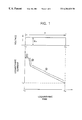
FIG. 1 and FIG. 2 are graphs showing accurately measured changes of current value, when direct current voltage is continuously applied to a ceramic capacitor, and when it is intermittently applied, respectively, logarithmic current value being plotted against time. In the case of continuous application, as shown by FIG. 1, a substantially constant large current flows during a very small time period (1) after a time t0 of starting application of a voltage E0. However, the current value is rapidly lowered successively during a transient time period (2) and thereafter, the current value is lowered with a linear charging characteristic (3) having an inclination. The linear charging characteristic (3) continues until about 1 to 2 minutes has elapsed since the start of charging.
In the case of intermittent application, as shown by FIG. 2, the characteristics (1),(2) and (3) are initially quite similar to those in the case of continuous application. Thereafter, a voltage E0 is applied a second time at time tb after voltage application is interrupted once at time ta. Although the current value is initially increased rapidly as shown by a curve (4), thereafter, the current value is rapidly lowered and is stabilized to a linear charging characteristic (5). Although the characteristic at the top of the curve (4) is not clearly shown, since the abscissa of FIG. 2 designates logarithmic time, the top portion is actually constituted by a horizontal portion similar to (1) and a transient period similar to (2). Further, it is found that the linear characteristic (5) is on a line extended from the linear charging characteristic (3) of the initial voltage application. Even when the intermittent application of voltage is repeated thereafter, characteristics similar to the above-described curves (4) and (5) are repeated and the current value is stabilized on the line extending from the linear charging characteristics (3) and (5). Incidentally, the value of applied voltage E0 is kept the same in the continuous application and the intermittent application.
A current value i3 at a time point t3 after a constant time period T has elapsed since the start of voltage application, stays the same in both the continuous application and the intermittent application. That is, even when the direct current is intermittently applied, as long as the OFF time (ta through tb for example) in the intermittent application is a short time period (for example, several hundreds of milliseconds or shorter), a result similar to continuous charging by the continuous application is provided.
According to an experiment conducted by the inventors, in the case of a capacitor having a capacitance value of 0.01 μF. or higher, when the OFF time of intermittent application is set to 500 m seconds or shorter, a result similar to that in the continuous application is provided.
A study of the above-described charging characteristic reveals the following fact. That is, the equivalent circuit of the capacitor is constituted by a capacitance C0, an equivalent series resistance r, an insulation resistance R0 and a dielectric polarized component D as shown by FIG. 3. It has been revealed that the nonlinear charging characteristics (1), (2) and (4) in FIG. 1 and FIG. 2 are attributed to the charging region of the capacitance C0 whereas the linear charging characteristics (3) and (5) are attributed to the charging region of the dielectric polarized component D.
Further, as mentioned above, when intermittent voltage application is performed, a result similar to that of continuous application is obtained and in this case, the charging rate of the capacitor remains unchanged.
Now, as a result of a further study on the intermittent application of direct current voltage to a capacitor, the inventors have found that a capacitor can be charged at a higher speed than in the case where direct current voltage is continuously applied, as long as certain conditions are satisfied. Based on these findings, the charging of a capacitor can be finished at a higher speed than in the case where the voltage is applied continuously, and the measurement of insulation resistance or determination of the quality or failure of the capacitor can be finished in a shorter period of time.
The present invention has been carried out based on the above-described knowledge and it is an advantage of the present invention to provide a method of charging a capacitor which is capable of charging at a high speed by intermittently applying direct current voltage to a capacitor.
In order to achieve the above-described object, according to the present invention, there is provided a method of charging a capacitor by intermittently applying a direct current voltage to a capacitor in which a voltage E1 applied in an initial application is larger than a voltage E2 applied in a succeeding application.
The inventors have obtained the results shown in FIG. 4 by charging the voltages applied in an intermittent application method. That is, in both the continuous application of FIG. 1 and the intermittent application of FIG. 2, a rated voltage E0 is applied. However, according to FIG. 4, an initial applied voltage E1 is made higher than the rated voltage, and an applied voltage E2 at a second time is set to the rated voltage.
In FIG. 4, although the initial characteristic curves of voltage application (1) through (3) at the first time are substantially the same as those in FIG. 1 and FIG. 2, when the voltage is applied for the second time, the current value is increased firstly as shown by a curve (6) and thereafter, the current value is rapidly lowered and is stabilized to a linear charging characteristic (7). The current value of the linear characteristic (7) is lower than the linear characteristic (5) in FIG. 2. That is, the characteristic (7) is not disposed on the extension of the characteristic (3). Further, when voltage is applied for the third time (voltage=E2), the current value is stabilized on the extension of the linear characteristic (7).
As described above, although the charging characteristics (1) through (3) obtained by the voltage application at a first time, are substantially the same as a charging characteristic obtained by applying a rated voltage, the charge current obtained by the voltage application E2 at a second time is considerably less than the charge current obtained by the rated voltage. That is, the charging progresses more rapidly than in the continuous application. Accordingly, although a time period of t3 is needed to reach the predetermined current value i3 in the continuous application or the intermittent application in which the rated voltage is applied, in contrast, in the intermittent application where the applied voltage is changed as described above, the required time period is reduced to t4. Thus, the charging time period can be shortened.
An investigation has been performed in respect of the ratio of the preceding applied voltage E1 to the succeeding applied voltage E2. It has been shown that a clear improvement is obtained when E1/E2≧1.2. Particularly, when E1/E2≧2, the charging progresses at a speed several times as much as in the case of E1=E2 by which the charging time period can significantly be shortened.
According to the present invention, there is provided the advantage that it is not necessary to stop operating a measuring device (for example, a turntable) for a long period of time as in the continuous application system. The insulation resistance can be measured while intermittently transferring capacitors. Accordingly, the equipment capacity can be improved.
Particularly, when a measuring device having a turntable is used, the charging region can be reduced and a number of terminals for measurement can be reduced.
Further, it has been found that a similar effect can be obtained even when a time period T1 of applying the voltage E1 is shortened, if the initial applied voltage E1 is increased. That is, an effect similar to that described above can be obtained even when the application time T1 of the initial applied voltage E1 is made shorter than the application time period T2 of the succeeding applied voltage E2 whereby the charging time period can further be shortened. Such an effect is effective in the case of a batch system wherein a predetermined number of capacitors are supplied to a turntable, the turntable is stopped, and charging and measurement of insulation resistance are simultaneously carried out in respect of the plurality of capacitors. Thus, the processing capacity in such a system can be improved.
In this case, it is necessary for the initial application time period T1 to be equal to or longer than a sum of the charging time period (1) and the transient time period (2) of the capacitor C0 to meet the requirement of measuring capacitors in a short period of time, and it is preferable that the initial application time period T1 be equal to or shorter than 100 milliseconds.
FIG. 1 is a charging characteristic diagram when direct current voltage is continuously applied to a capacitor;
FIG. 2 is a charging characteristic diagram when direct current voltage is intermittently applied to a capacitor;
FIG. 3 is an equivalent circuit diagram of a capacitor;
FIG. 4 is a charging characteristic diagram when direct current voltage is intermittently applied to a capacitor in accordance with the method according to an embodiment of the present invention;
FIG. 5 is a circuit diagram of an example of a current measuring device;
FIG. 6 is a diagram showing an example of an intermittent application method;
FIG. 7 is an actual charging characteristic diagram when the intermittent application of FIG. 6 is carried out;
FIG. 8 is a flow chart of a method of determining the quality of a product using a charging method according to the present invention; and
FIG. 9 is a plan view of an example of a characteristic measuring and selecting device using the method of the present invention.
FIG. 5 shows an example of a current measuring device for performing a method according to an embodiment of the present invention. The measuring device has been suggested by the applicant in Japanese Application No. 7-293442.
The measuring device is provided with direct current power sources 10 a and 10 b, a switch 11, a capacitor 12 that is an object for measurement, a current control resistor 13, a logarithmic amplifier 14, an instrumentation amplifier 15, A/D (Analog to Digital) converters 16 and 18 and a calculation processing circuit (CPU) 17. At the initial stage of charging, a current value is measured by the instrumentation amplifier 15 and the current is switched to the logarithmic amplifier 14 in accordance with a predetermined threshold and thereafter, measured by the logarithmic amplifier 14. The measuring device can accurately measure the charging current of the capacitor 12 even if the current is varied over a wide range of the width and therefore, the current value from the initial stage of charging to the final stage of charging which has been difficult to measure by a conventional measuring device can continuously be measured.
The switch 11 is switched by CPU 17 at predetermined time intervals by which a direct current voltage is intermittently applied to the capacitor 12 from either of the direct current measuring power sources 10 a and 10 b. A voltage E2 of the power source 10 b is set to a rated voltage (in this case, 25 volts) and a voltage E1 of the power source 10 a is set to be higher than the voltage E2.
A time interval for making the switch 11 ON/OFF may not necessarily be constant. For example, the ON time at a second time may be longer than the ON time at a first time or the ON time at the first time may be longer than the ON time at the second time. Further, when the voltage is applied three times or more, the ON times at respective times may be changed. The respective intervals between ON times also may not be constant.
Incidentally, the method of the present invention does not need to use the measuring device of FIG. 5 but may use any other device as long as different voltages can be intermittently applied to the capacitor.
Next, FIG. 7 shows charging characteristics in a case A where the rated voltage (25 volts) is intermittently applied twice as shown by FIG. 2 and cases B and C where different current voltages E1 and E2 are intermittently applied as shown by FIG. 6. In this case, a multi-layered ceramic capacitor is used for the capacitor and an initial charging current is set to 50 mA. Further, in experiments A through C, an application (ON) time period at a first time is set to T1=20 m seconds, an open (OFF) time period is set to T3=20 m seconds and an application (ON) time period at a second time is set to T2=1 second and respective voltages are specified below.
| TABLE 1 | |||||
| Experimental example | A | B | C | ||
| 1st time (E1) | 25 V | 30 V | 50 V | ||
| 2nd time (E2) | 25 V | 25 V | 25 V | ||
As is apparent from FIG. 7, although the charging characteristic at the first voltage application stays substantially the same in either of the cases A through C, in the second voltage application, the charge current values are in a relationship of A>B>C and the charging progresses the fastest in case C. Also, in case B, the charging progresses faster than in case A. A time period required for lowering the charging current value to 1×10⁻⁷A or lower is about 0.8 second in case A, about 0.4 second in case B and about 0.16 second in case C whereby it is seen that high speed charging has been performed in cases B and C compared with case A.
As a result of conducting a further experiment in the case of E1/E2>2, it has been shown that the charging rate is increased with an increase in E1/E2. Further, it has also been shown that when the applied voltages at the first time and the second time are made larger than the rated voltage, only a characteristic similar to that in FIG. 2 can be obtained as long as the applied voltages at the first time and the second time are set to the same voltage.
Further, it has been confirmed that a similar effect is obtained even if the first application time T1 is made shorter than the second application time T2. Therefore, the charging time can further be shortened. However, the time period T1 is varied by the capacitance of the capacitor and a condition of an upper limit of T1 must be established as follows:
Further, it is preferable that T1 have the following upper limit value in order to measure the multi-layered ceramic capacitor in a short period of time:
Further, the time period T2 may be determined arbitrarily from the requested processing capacity of the object for measurement.
An explanation will be given of a method of determining quality or failure rate by using the method of the present invention in reference to FIG. 8.
First, the intermittent application using different voltages E1, E2 . . . is performed (step S1).
Next, it is determined whether a time period “t” elapsed from start of voltage application, has elapsed a predetermined time period tc (step S2). The time period tc is a reference time period where the charging current reaches a threshold ic by the intermittent application and the time period tc is set to, for example, about 1 to 10 seconds. When the predetermined time period tc has not elapsed, the intermittent application is repeated.
After the predetermined time period tc has elapsed, a current value i (t) is measured (step S3) and the current value i (t) is compared with the threshold ic for determining quality or failure (step S4).
When i(t)<ic, it is determined that the object is an excellent product since the charging has sufficiently been progressed (step S5) and when i(t)≧ic, the object is determined to be a failed product since the charging has not been progressed sufficiently (step S6).
Incidentally, no limitation is imposed on whether the insulation resistance is measured after charging the capacitor in accordance with the method of the present invention, or whether quality or failure is determined, by comparing the current value after the capacitor has been charged for a predetermined time period with the threshold.
FIG. 9 shows a specific example of a characteristic measuring and selecting device using the method of the present invention.
The charge unit 24 is separated into a plurality of stages in which, for example, an applied voltage at an earlier half portion 24 a is set to E1 and an applied voltage at a later half portion 24 b is set to E2. Although in this case, a plurality of times of voltage application is performed for each of the portions 24 a and 24 b, the voltage application may be performed only once for each thereof.
Although in the conventional case, the charging region needs to be widened since a long period of time of charging must be performed in respect of capacitors on the turntable and therefore, the turntable per se is large-sized, when the method of the present invention is used, the charging region 24 need not be widened since the capacitors can be charged at a high speed and therefore, the turntable 20 can be downsized, the number of terminals for measurement can be reduced and cost reduction can be achieved. Further, a portion which has been the charging region can be used for other uses such as characteristic measurement or the like.
Further, the present invention is not limited to charging of a ceramic capacitor but can be used in charging other capacitors such as an electrolytic capacitor, a film capacitor and the like.
Further, various patterns are conceivable for patterns of voltage application according to the present invention. The number of times the preceding voltage application is applied E1 and the number of times the succeeding voltage E2 is applied are not limited to one but may be a plurality of times. For example, large and small voltage applications may be repeated a plurality of times, such as voltage application E1 at a first time, voltage application E2 at a second time (E2<E1), voltage application E1 at a third time and voltage application E2 at a fourth time. Or, a relationship among voltage application E1 at a first time, voltage application E2 at a second time and voltage application E3 at a third time may be specified by E3<E2<E1. In any case, the charging is accelerated by performing application of a small voltage after application of the large voltage and therefore, stages of application of a small voltage after application of a large voltage may preferably be included.
As is apparent from the above-described explanation, according to the present invention, a direct current voltage is intermittently applied to a capacitor such that the preceding applied voltage E1 is made larger than the succeeding applied voltage E2 and therefore, charging swiftly progresses during the open period and charging can be performed at a higher speed than when continuously applying the voltage. As a result, it is possible to finish measurement of insulation resistance and determination of quality or failure at a higher speed, thereby significantly promoting measurement capacity.
Claims (5)
1. A method of charging a capacitor by intermittently applying a direct current voltage to the capacitor, comprising the steps of:
initially applying a voltage E1 to the capacitor; and then applying a voltage E2 to the capacitor, wherein E2 is smaller than E1.
2. The method of charging a capacitor according to claim 1, wherein the initial applied voltage E1 is not less than 1.2 times as large as the succeeding applied voltage E2.
3. The method of charging a capacitor according to claim 2:
wherein an application time period T1 of the initial applied voltage E1 is shorter than an application time period T2 of the succeeding applied voltage E2; and
wherein the initial application time period T1 is equal to or longer than a sum of a charging time period (1) of a capacitance C0 of the capacitor, and a transient time period (2) of the capacitance C0 of the capacitor, and equal to or shorter than 100 milliseconds.
4. The method of charging a capacitor according to claim 1:
wherein an application time period T1 of the initial applied voltage E1 is shorter than an application time period T2 of the succeeding applied voltage E2; and
wherein the initial application time period T1 is equal to or longer than a sum of a charging time period (1) of a capacitance C0 of the capacitor, and a transient time period (2) of the capacitance C0 of the capacitor, and equal to or shorter than 100 milliseconds.
5. The method of charging a capacitor according to claim 1, wherein E1 is greater than a rated voltage of the capacitor and E2 is substantially equal to the rated voltage of the capacitor.
Priority Applications (1)
| Application Number | Priority Date | Filing Date | Title |
|---|---|---|---|
| US09/187,598 US6066940A (en) | 1997-01-06 | 1998-11-06 | Capacitor charging method |
Applications Claiming Priority (2)
| Application Number | Priority Date | Filing Date | Title |
|---|---|---|---|
| JP9-12021 | 1997-01-06 | ||
| JP1202197 | 1997-01-06 |
Related Child Applications (1)
| Application Number | Title | Priority Date | Filing Date |
|---|---|---|---|
| US09/187,598 Continuation-In-Part US6066940A (en) | 1997-01-06 | 1998-11-06 | Capacitor charging method |
Publications (1)
| Publication Number | Publication Date |
|---|---|
| US6204638B1 true US6204638B1 (en) | 2001-03-20 |
Family
ID=11793955
Family Applications (1)
| Application Number | Title | Priority Date | Filing Date |
|---|---|---|---|
| US09/003,263 Expired - Lifetime US6204638B1 (en) | 1997-01-06 | 1998-01-06 | Method for charging capacitor |
Country Status (4)
| Country | Link |
|---|---|
| US (1) | US6204638B1 (en) |
| KR (1) | KR100308768B1 (en) |
| MY (1) | MY120013A (en) |
| SG (1) | SG70060A1 (en) |
Cited By (3)
| Publication number | Priority date | Publication date | Assignee | Title |
|---|---|---|---|---|
| US20040251880A1 (en) * | 2003-06-10 | 2004-12-16 | O'brien Robert Neville | Battery charging method using supercapacitors at two stages |
| US6972921B1 (en) | 2004-04-05 | 2005-12-06 | Marvell International Ltd. | Circuit and method for protecting emergency head-retract |
| EP2103950A1 (en) * | 2008-03-19 | 2009-09-23 | Humo Laboratory, Ltd. | Method for inspecting insulation property of capacitor |
Citations (8)
| Publication number | Priority date | Publication date | Assignee | Title |
|---|---|---|---|---|
| US4149533A (en) | 1976-10-13 | 1979-04-17 | Matsushita Electric Industrial Co., Ltd. | Device for iontophoretic application of fluoride on tooth |
| US4284944A (en) * | 1978-10-12 | 1981-08-18 | Matsushita Electric Works, Ltd. | Battery charging device having battery state indicating function |
| JPH04254769A (en) | 1991-02-05 | 1992-09-10 | Murata Mfg Co Ltd | Method for measuring characteristic of electronic parts |
| US5617007A (en) * | 1994-08-17 | 1997-04-01 | International Business Machines Corporation | Battery charging method and apparatus using current control |
| JPH09113545A (en) | 1995-10-16 | 1997-05-02 | Murata Mfg Co Ltd | Electric current measuring device |
| US5646506A (en) * | 1996-08-21 | 1997-07-08 | Suzuki; Takeshi | Method of charging a secondary battery and an apparatus therefor |
| US5659239A (en) * | 1995-10-05 | 1997-08-19 | Saft | Method and apparatus for charging sealed nickel-cadmium batteries |
| US5694023A (en) * | 1996-07-10 | 1997-12-02 | Advanced Charger Technology, Inc. | Control and termination of a battery charging process |
Family Cites Families (1)
| Publication number | Priority date | Publication date | Assignee | Title |
|---|---|---|---|---|
| LU77252A1 (en) * | 1976-05-06 | 1977-08-22 |
-
1998
- 1998-01-02 SG SG1998000018A patent/SG70060A1/en unknown
- 1998-01-03 MY MYPI98000018A patent/MY120013A/en unknown
- 1998-01-06 US US09/003,263 patent/US6204638B1/en not_active Expired - Lifetime
- 1998-01-06 KR KR1019980000074A patent/KR100308768B1/en active IP Right Grant
Patent Citations (9)
| Publication number | Priority date | Publication date | Assignee | Title |
|---|---|---|---|---|
| US4149533A (en) | 1976-10-13 | 1979-04-17 | Matsushita Electric Industrial Co., Ltd. | Device for iontophoretic application of fluoride on tooth |
| US4284944A (en) * | 1978-10-12 | 1981-08-18 | Matsushita Electric Works, Ltd. | Battery charging device having battery state indicating function |
| JPH04254769A (en) | 1991-02-05 | 1992-09-10 | Murata Mfg Co Ltd | Method for measuring characteristic of electronic parts |
| US5262729A (en) | 1991-02-05 | 1993-11-16 | Murata Manufacturing Co., Ltd. | Method of measuring characteristics of electronic parts |
| US5617007A (en) * | 1994-08-17 | 1997-04-01 | International Business Machines Corporation | Battery charging method and apparatus using current control |
| US5659239A (en) * | 1995-10-05 | 1997-08-19 | Saft | Method and apparatus for charging sealed nickel-cadmium batteries |
| JPH09113545A (en) | 1995-10-16 | 1997-05-02 | Murata Mfg Co Ltd | Electric current measuring device |
| US5694023A (en) * | 1996-07-10 | 1997-12-02 | Advanced Charger Technology, Inc. | Control and termination of a battery charging process |
| US5646506A (en) * | 1996-08-21 | 1997-07-08 | Suzuki; Takeshi | Method of charging a secondary battery and an apparatus therefor |
Cited By (8)
| Publication number | Priority date | Publication date | Assignee | Title |
|---|---|---|---|---|
| US20040251880A1 (en) * | 2003-06-10 | 2004-12-16 | O'brien Robert Neville | Battery charging method using supercapacitors at two stages |
| US6836098B1 (en) * | 2003-06-10 | 2004-12-28 | O'brien Robert Neville | Battery charging method using supercapacitors at two stages |
| US6972921B1 (en) | 2004-04-05 | 2005-12-06 | Marvell International Ltd. | Circuit and method for protecting emergency head-retract |
| US7116512B1 (en) | 2004-04-05 | 2006-10-03 | Marvell International Ltd. | Circuit and method for protecting emergency head-retract capacitor in a hard disk drive |
| US7436618B1 (en) | 2004-04-05 | 2008-10-14 | Marvell International Ltd. | Circuit and method for protecting emergency head-retract capacitor in a hard disk drive |
| US7623316B1 (en) | 2004-04-05 | 2009-11-24 | Marvell International Ltd. | Circuit and method for protecting emergency head-retract capacitor in a hard disk drive |
| EP2103950A1 (en) * | 2008-03-19 | 2009-09-23 | Humo Laboratory, Ltd. | Method for inspecting insulation property of capacitor |
| US20090237088A1 (en) * | 2008-03-19 | 2009-09-24 | Humo Laboratory, Ltd. | Method for inspecting insulation property of capacitor |
Also Published As
| Publication number | Publication date |
|---|---|
| KR100308768B1 (en) | 2001-11-30 |
| MY120013A (en) | 2005-08-30 |
| SG70060A1 (en) | 2000-01-25 |
| KR19980070346A (en) | 1998-10-26 |
Similar Documents
| Publication | Publication Date | Title |
|---|---|---|
| DE60023772T2 (en) | Device with several electric double-layer capacitors and method for adjusting the capacitor voltages | |
| US4686628A (en) | Electric device or circuit testing method and apparatus | |
| DE19821195A1 (en) | Control circuit for balancing steady state current in each component of electric power converter | |
| US20080143342A1 (en) | Screening of electrolytic capacitors | |
| JP2007333529A (en) | Insulation resistance measuring apparatus, leakage current measuring apparatus, insulation resistance measurement method and leakage current measurement method | |
| KR20030030035A (en) | Capacitor insulation resistance measuring method and insulation resistance measuring instrument | |
| US6204638B1 (en) | Method for charging capacitor | |
| US6384609B1 (en) | Method of measuring insulation resistance of capacitors | |
| JP3156658B2 (en) | How to charge a capacitor | |
| US6521166B1 (en) | Method of polarization-treating piezoelectric body | |
| US4691337A (en) | Method and apparatus for determining the value of analog voltages occurring on telephone subscriber lines of a digital telephone exchange | |
| US6066940A (en) | Capacitor charging method | |
| US3635802A (en) | Method of anodizing a thin-film device | |
| KR100299938B1 (en) | Capacitor charging method | |
| US5181154A (en) | Circuit arrangement for optimal current generation in processes of electrochemically initiated plasma-chemical layer production | |
| JPH10115651A (en) | Inspection method for leak current characteristic of capacitor | |
| US4399401A (en) | Method for destructive testing of dielectric ceramic capacitors | |
| US20170197267A1 (en) | Wire electrical discharge machine with deterioration detection function for feeder | |
| Howard et al. | Dielectric breakdown in solid electrolyte tantalum capacitors | |
| SU942183A1 (en) | Method of rejecting oxide-semiconductor capacitors | |
| RU1759041C (en) | Apparatus for metals and alloys microarc weld oxide coating | |
| KR840000673B1 (en) | Power source for a wire-cut electric discharge machine | |
| KR0122106B1 (en) | Discharge circuit of electrolytic condenser | |
| KR20230089426A (en) | Substrate inspecting device using artificial intelligence | |
| JPH0714742A (en) | Screening method for ceramic electronic component |
Legal Events
| Date | Code | Title | Description |
|---|---|---|---|
| AS | Assignment |
Owner name: MURATA MANUFACTURING CO., LTD., JAPAN Free format text: ASSIGNMENT OF ASSIGNORS INTEREST;ASSIGNORS:NISHIOKA, YOSHINAO;TABATA, TOSHINARI;REEL/FRAME:008926/0558 Effective date: 19971215 |
|
| FEPP | Fee payment procedure |
Free format text: PAYOR NUMBER ASSIGNED (ORIGINAL EVENT CODE: ASPN); ENTITY STATUS OF PATENT OWNER: LARGE ENTITY |
|
| STCF | Information on status: patent grant |
Free format text: PATENTED CASE |
|
| FPAY | Fee payment |
Year of fee payment: 4 |
|
| FPAY | Fee payment |
Year of fee payment: 8 |
|
| FPAY | Fee payment |
Year of fee payment: 12 |