US6191609B1 - Combination of global clock and localized clocks - Google Patents
Combination of global clock and localized clocks Download PDFInfo
- Publication number
- US6191609B1 US6191609B1 US09/433,642 US43364299A US6191609B1 US 6191609 B1 US6191609 B1 US 6191609B1 US 43364299 A US43364299 A US 43364299A US 6191609 B1 US6191609 B1 US 6191609B1
- Authority
- US
- United States
- Prior art keywords
- logic device
- clock
- programmable logic
- localized
- global clock
- Prior art date
- Legal status (The legal status is an assumption and is not a legal conclusion. Google has not performed a legal analysis and makes no representation as to the accuracy of the status listed.)
- Expired - Lifetime
Links
Images


Classifications
-
- H—ELECTRICITY
- H03—ELECTRONIC CIRCUITRY
- H03K—PULSE TECHNIQUE
- H03K19/00—Logic circuits, i.e. having at least two inputs acting on one output; Inverting circuits
- H03K19/02—Logic circuits, i.e. having at least two inputs acting on one output; Inverting circuits using specified components
- H03K19/173—Logic circuits, i.e. having at least two inputs acting on one output; Inverting circuits using specified components using elementary logic circuits as components
- H03K19/177—Logic circuits, i.e. having at least two inputs acting on one output; Inverting circuits using specified components using elementary logic circuits as components arranged in matrix form
- H03K19/17736—Structural details of routing resources
- H03K19/1774—Structural details of routing resources for global signals, e.g. clock, reset
-
- G—PHYSICS
- G06—COMPUTING; CALCULATING OR COUNTING
- G06F—ELECTRIC DIGITAL DATA PROCESSING
- G06F1/00—Details not covered by groups G06F3/00 - G06F13/00 and G06F21/00
- G06F1/04—Generating or distributing clock signals or signals derived directly therefrom
- G06F1/10—Distribution of clock signals, e.g. skew
Definitions
- the present invention relates generally to semiconductor integrated circuits, and more particularly, to a combination of a global clock and localized clocks.
- a programmable logic device is a standard product which can be purchased by systems manufacturers in a “blank” state and, thereafter, custom-configured into a virtually unlimited number of specific logic functions by programming the device. Because programmable logic devices provide great flexibility, these devices can be incorporated into a variety of systems.
- the performance at which any such system can be operated is a function, at least in part, of the set-up time (T SU ) and clock-to-output delay time (T CO ) of the clock signals supplied to programmable logic device.
- the set-up time is the amount of time that information or data must be present at an input terminal before it can be latched and stored in the input registers of the programmable logic device.
- the clock-to-output delay time is the time that it takes for data to be present at an output terminal after a clock occurs.
- the operating frequency for the device is limited by the reciprocal of the sum of the set-up time and the clock-to-output delay time. This relationship is set out in the following equation:
- ⁇ OP is the operating frequency. Consequently, in order to maximize the operating frequency for the system, and hence, its performance, both the set-up time and the clock-to-output delay time should be minimized.
- the set-up time for a programmable logic device can not be decreased without producing a corresponding increase in the clock-to-output delay time.
- a single global clock is used to drive both input and output signals at all locations of the device.
- a clock distribution structure comprising various lines, buffers, and other circuitry distributes the global clock so that it can be presented substantially simultaneously to all parts of the logic device. With this distribution, a delay in the global clock is created. This delay affects both the set-up time and the clock-to-output delay time.
- the set-up time can be decreased if the delay is longer.
- a longer delay in the global clock causes the clock-to-output delay time to be increased. Accordingly, any improvement in performance that would otherwise be provided by a decrease in set-up time is offset by a corresponding increase in clock-to-output delay time.
- a programmable logic device includes a global clock structure and a plurality of localized clock structures.
- the global clock structure distributes a global clock signal throughout the programmable logic device.
- Each localized clock structure distributes a respective localized clock signal to a corresponding portion of the programmable logic device.
- Important technical advantages of the present invention include providing both a global clock and a number of localized clocks on a programmable logic device.
- Each of the localized clocks is distributed and available only to a respective portion of the programmable logic device.
- the global clock is distributed throughout the device and available to all portions.
- the localized clocks and the global clock may each experience some delay, but the delay for the localized clocks will be less due to the smaller areas of distribution.
- the global clock is used to drive input registers for the programmable logic device, while the localized clocks are used to drive output registers in the respective portions.
- the input data set-up time for the programmable logic device is determined by the global clock, whereas the clock-to-output delay time is determined by the localized clocks.
- the set-up time is the time that data must be applied to the device input before the active edge of the global clock is applied to the global clock input.
- the clock-to-output delay time is the time it takes for data to appear at the device output after the local clock is applied to the local clock input.
- the set-up time can be decreased due to the longer delay of the global clock. Furthermore, due to the shorter delay and independence of the localized clocks, the clock-to-output delay time can be decreased as well. Accordingly, a system incorporating the programmable logic device may be operated at a higher frequency, thereby enhancing performance.
- FIG. 1 illustrates a layout for a programmable logic device which utilizes a combination of a global clock and multiple localized clocks, in accordance with an embodiment of the present invention
- FIG. 2 illustrates a layout for a programmable logic device which utilizes a combination of a global clock and multiple localized clocks, in accordance with another embodiment of the present invention.
- FIG. 3 is a timing diagram for various signals in a programmable logic device which utilizes a global clock and one or more localized clocks, in accordance with the present invention.
- FIGS. 1 through 3 of the drawings Like numerals are used for like and corresponding parts of the various drawings.
- FIG. 1 illustrates a layout for a programmable logic device 10 which utilizes a combination of a global clock and multiple localized clocks, in accordance with an embodiment of the present invention.
- each localized clock is available to drive only elements which are located in a respective portion of programmable logic device 10
- the global clock is available to drive elements in all portions of the device.
- programmable logic device 10 comprises a global clock structure 12 and a plurality of localized clock structures 14 .
- Global clock structure 12 generally functions to distribute and uniformly present a global clock signal throughout programmable logic device 10 .
- global clock structure 12 includes a pin 16 , located in the middle of one edge or side of device 10 , at which an input clock signal can be received.
- a line 18 is connected to pin 16 .
- the terms “connected,” “coupled,” or any variant thereof, means any connection or coupling, either direct or indirect, between two or more elements.
- Line 18 carries the input clock signal to a central point 20 in programmable logic device 10 . From central point 20 , the input clock signal is carried by lines 22 to the periphery or various sides of programmable logic device 10 . Lines 22 and 24 make the clock signal available throughout the whole device.
- a global clock structure on a programmable logic device has been shown and described, it should be understood that any other suitable implementation can be used.
- another implementation may comprise a pin and one or more conductive lines which follow the edges of a logic device.
- more than one global clock may be provided on a programmable logic device.
- various circuitry comprising buffers, drivers, and the like, are connected to global clock structure 12 .
- This circuitry buffers the input clock signal along lines 18 , 22 , and 24 so that the input clock signal can be distributed and then presented simultaneously throughout all portions of programmable logic device 10 as the global clock signal. Due to this buffering and distribution, an input signal experiences some delay before it is presented as the global clock signal.
- Each localized clock structure 14 functions to distribute a respective localized clock signal in a corresponding portion of programmable logic device 10 .
- each localized clock structure 14 is located in and supports a separate side of logic device 10 .
- Localized clock structures 14 each comprise a separate pin 26 located approximately in the middle of the respective side. Each of these pins 26 may receive a respective input clock signal, or alternatively, at least two of pins 26 may be connected together externally on a board to receive the same input clock signal.
- the respective input clock signals can be the same or separate for the various localized clock structures 14 .
- Lines 28 extend in opposite directions from each pin 26 along the respective sides. These lines 28 make each of the various input clock signals available on the respective side as a respective localized clock signal.
- Each respective input clock signal experiences some delay before it is presented as a respective localized clock signal. Due to the smaller area of distribution, however, this delay in the localized clock signals is not as great as the delay for the global clock signal.
- a plurality of input/output (I/O) cells 30 are located at the periphery or sides of programmable logic device 10 .
- I/O cells 30 function to store or hold information input into or output from logic device 10 .
- each I/O cell 30 comprises one or more registers connected to corresponding pins (not shown for the sake of clarity). The pins and registers can be programmed by an end user to support either input or output.
- Each I/O cell 30 may be driven by the global clock, supported by global clock structure 12 , and one of the localized clocks, supported by the localized clock structure 14 on the respective side.
- appropriate connections are provided between each I/O cell 30 and the clock structures which drive it.
- a logic section 32 is centrally located on programmable logic device 10 . That is, logic section 32 is situated within the periphery defined by I/O cells 30 . Although not explicitly shown, logic section 32 is connected to each I/O cell 30 . In general, logic section 32 may perform any one or a combination of various operations upon bits of information received, stored, and/or generated within programmable logic device 10 . At least a portion of this information can be input or output from logic device 10 at the registers and pins of I/O cells 30 .
- a respective input clock signal is applied to each of global clock structure 12 and localized clock structures 14 .
- the input clock signal received by global clock structure 12 is buffered, distributed, and then presented simultaneously throughout programmable logic device 10 as the global clock signal.
- the global clock is preferably used to drive the input registers to receive the input of data at all I/O cells 30 of the logic device.
- the respective input clock signal for each localized clock structure 14 is distributed and presented in the corresponding portion of programmable logic device 10 as a respective localized clock signal.
- Each of the localized clocks is preferably used to drive the output registers to send output data at any I/O cells 30 located in the corresponding portion.
- the localized clocks and the global clock may each experience some delay.
- an input clock signal applied at pin 16 of global clock structure 12 is delayed because it must be carried or distributed across lines 18 , 22 , and 24 .
- an input clock signal applied at pin 26 of a particular localized clock structure 14 is delayed as the signal is distributed along respective lines 28 .
- the delay for each of the localized clocks can be less than that for the global clock because the distribution along lines 28 for each localized clock is shorter than the distribution along lines 18 , 22 , and 24 for the global clock.
- the set-up time for programmable logic device 10 is determined by the global clock, whereas the clock-to-output delay time is determined by the localized clocks.
- the set-up time can be decreased due to the longer delay of the global clock. Furthermore, due to the shorter delay and independence of the localized clocks, the clock-to-output delay time can be decreased as well. Accordingly, a system incorporating programmable logic device 10 may be operated at a higher frequency, thereby enhancing performance.
- the global clock can also be used instead of, or in addition to, the localized clocks to drive at least some of the output registers to send output data at any I/O cells 30 .
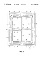
- FIG. 2 illustrates a layout for a programmable logic device 40 which utilizes a combination of a global clock and multiple localized clocks, in accordance with another embodiment of the present invention.
- Programmable logic device 40 includes a global clock structure 42 and a plurality of localized clock structures 44 for supporting the global clock and the multiple localized clocks, respectively.
- Global clock structure comprises pin 46 , line 48 , central point 50 , lines 52 , and lines 54 .
- Each localized clock structure 44 comprises a pin 56 with lines 58 extending therefrom.
- Programmable logic device 40 also includes a number of I/O cells 60 and a logic section 62 .
- These elements of programmable logic device 40 are substantially similar to the elements referred to by like names in the description for programmable logic device 10 of FIG. 1 . Significant differences between the elements of programmable logic device 40 and programmable logic device 10 are as follows.
- pins 56 of the respective localized clock structures 44 are located at the comers of the device. Lines 58 extend from each pin 56 along the respective sides which define each comer. Due to this arrangement, each localized clock structure 44 supports I/O cells 60 located in the respective comers.
- Programmable logic device 40 operates in a manner similar to programmable logic device 10 shown in FIG. 1, and thus, provides substantially the same advantages.
- input clock signals are applied to each of global clock structure 42 and localized clock structures 44 to produce a global clock and a plurality of localized clocks, respectively.
- the global clock is preferably used to drive the input registers to receive data at all I/O cells 60 .
- Each of the localized clocks is preferably used to drive the output registers to send output data at any I/O cells 60 located in the corresponding comers.
- the global clock and the localized clocks may experience some delay, but the delay for the localized clocks is not as great as that for the global clock.
- the set-up time for programmable logic device 40 can be decreased due to the larger delay of the global clock. Furthermore, due to the shorter delay and independence of the localized clocks, the clock-to-output delay time can be decreased as well. Accordingly, a system incorporating programmable logic device 40 may be operated at a high frequency, thereby enhancing performance.
- FIG. 3 is a timing diagram for various signals in a programmable logic device which utilizes a global clock and one or more localized clocks, in accordance with the present invention.
- an input clock signal 100 has the form of a clock signal with a repeating high and low pattern.
- a global clock signal 102 may be generated from input clock signal 100 .
- the input clock signal may be distributed via a global clock structure and presented as the global clock signal to all portions of the programmable logic device. Due to this distribution, a time delay t 1 is created between input clock signal 100 and global clock signal 102 .
- a localized clock signal 104 may also be generated from input clock signal 100 .
- the input clock signal can be distributed via a localized clock structure and presented in a respective portion of the programmable logic device as the localized clock signal. Due to the distribution in the localized clock structure, a time delay t 2 is created between input clock signal 100 and localized clock signal 104 .
- Time delay t 2 associated with localized clock signal 104 is less than time delay t 1 associated with the global clock signal 102 . This difference in delay times is due to the fact that the localized clock structure distributes in a smaller area than the global clock structure.
- the localized clock signal 104 it is advantageous to use the localized clock signal 104 to drive the output from the I/O cells of the programmable logic device.
- time delay t 2 is smaller, the output from programmable logic device can be sent out more rapidly than would be the case if the global clock signal 102 was used to perform this function.
Abstract
Description
Claims (2)
Priority Applications (1)
| Application Number | Priority Date | Filing Date | Title |
|---|---|---|---|
| US09/433,642 US6191609B1 (en) | 1998-04-27 | 1999-11-03 | Combination of global clock and localized clocks |
Applications Claiming Priority (2)
| Application Number | Priority Date | Filing Date | Title |
|---|---|---|---|
| US09/069,035 US6133750A (en) | 1998-04-27 | 1998-04-27 | Combination of global clock and localized clocks |
| US09/433,642 US6191609B1 (en) | 1998-04-27 | 1999-11-03 | Combination of global clock and localized clocks |
Related Parent Applications (1)
| Application Number | Title | Priority Date | Filing Date |
|---|---|---|---|
| US09/069,035 Division US6133750A (en) | 1998-04-27 | 1998-04-27 | Combination of global clock and localized clocks |
Publications (1)
| Publication Number | Publication Date |
|---|---|
| US6191609B1 true US6191609B1 (en) | 2001-02-20 |
Family
ID=22086309
Family Applications (2)
| Application Number | Title | Priority Date | Filing Date |
|---|---|---|---|
| US09/069,035 Expired - Lifetime US6133750A (en) | 1998-04-27 | 1998-04-27 | Combination of global clock and localized clocks |
| US09/433,642 Expired - Lifetime US6191609B1 (en) | 1998-04-27 | 1999-11-03 | Combination of global clock and localized clocks |
Family Applications Before (1)
| Application Number | Title | Priority Date | Filing Date |
|---|---|---|---|
| US09/069,035 Expired - Lifetime US6133750A (en) | 1998-04-27 | 1998-04-27 | Combination of global clock and localized clocks |
Country Status (1)
| Country | Link |
|---|---|
| US (2) | US6133750A (en) |
Cited By (4)
| Publication number | Priority date | Publication date | Assignee | Title |
|---|---|---|---|---|
| US6996736B1 (en) * | 2001-05-06 | 2006-02-07 | Altera Corporation | Programmable clock network for distributing clock signals to and between first and second sections of an integrated circuit |
| US7737751B1 (en) * | 2006-08-25 | 2010-06-15 | Altera Corporation | Periphery clock distribution network for a programmable logic device |
| US7821295B1 (en) | 2009-03-27 | 2010-10-26 | Altera Corporation | Methods and systems for improving a maximum operating frequency of a PLD having a shift register within an embedded memory block |
| US8191028B1 (en) | 2009-04-07 | 2012-05-29 | Altera Corporation | Methods and systems for improving a maximum operating frequency of an integrated circuit during a route phase |
Families Citing this family (5)
| Publication number | Priority date | Publication date | Assignee | Title |
|---|---|---|---|---|
| DE10144070A1 (en) * | 2001-09-07 | 2003-03-27 | Philips Corp Intellectual Pty | Communication network and method for controlling the communication network |
| US6911842B1 (en) * | 2002-03-01 | 2005-06-28 | Xilinx, Inc. | Low jitter clock for a physical media access sublayer on a field programmable gate array |
| CN1784325A (en) * | 2003-05-06 | 2006-06-07 | 皇家飞利浦电子股份有限公司 | Timeslot sharing over different cycles in tdma bus |
| US6856171B1 (en) | 2003-06-11 | 2005-02-15 | Lattice Semiconductor Corporation | Synchronization of programmable multiplexers and demultiplexers |
| US9032358B2 (en) | 2013-03-06 | 2015-05-12 | Qualcomm Incorporated | Integrated circuit floorplan for compact clock distribution |
Citations (5)
| Publication number | Priority date | Publication date | Assignee | Title |
|---|---|---|---|---|
| US4903223A (en) * | 1988-05-05 | 1990-02-20 | Altera Corporation | Programmable logic device with programmable word line connections |
| US4912342A (en) * | 1988-05-05 | 1990-03-27 | Altera Corporation | Programmable logic device with array blocks with programmable clocking |
| US5140184A (en) * | 1989-12-07 | 1992-08-18 | Hitachi, Ltd. | Clock feeding circuit and clock wiring system |
| US5396129A (en) * | 1992-05-25 | 1995-03-07 | Matsushita Electronics Corporation | Semiconductor integrated circuit apparatus comprising clock signal line formed in a ring shape |
| US5668484A (en) * | 1993-09-24 | 1997-09-16 | Nec Corporation | High frequency clock signal distribution circuit with reduced clock skew |
-
1998
- 1998-04-27 US US09/069,035 patent/US6133750A/en not_active Expired - Lifetime
-
1999
- 1999-11-03 US US09/433,642 patent/US6191609B1/en not_active Expired - Lifetime
Patent Citations (5)
| Publication number | Priority date | Publication date | Assignee | Title |
|---|---|---|---|---|
| US4903223A (en) * | 1988-05-05 | 1990-02-20 | Altera Corporation | Programmable logic device with programmable word line connections |
| US4912342A (en) * | 1988-05-05 | 1990-03-27 | Altera Corporation | Programmable logic device with array blocks with programmable clocking |
| US5140184A (en) * | 1989-12-07 | 1992-08-18 | Hitachi, Ltd. | Clock feeding circuit and clock wiring system |
| US5396129A (en) * | 1992-05-25 | 1995-03-07 | Matsushita Electronics Corporation | Semiconductor integrated circuit apparatus comprising clock signal line formed in a ring shape |
| US5668484A (en) * | 1993-09-24 | 1997-09-16 | Nec Corporation | High frequency clock signal distribution circuit with reduced clock skew |
Cited By (4)
| Publication number | Priority date | Publication date | Assignee | Title |
|---|---|---|---|---|
| US6996736B1 (en) * | 2001-05-06 | 2006-02-07 | Altera Corporation | Programmable clock network for distributing clock signals to and between first and second sections of an integrated circuit |
| US7737751B1 (en) * | 2006-08-25 | 2010-06-15 | Altera Corporation | Periphery clock distribution network for a programmable logic device |
| US7821295B1 (en) | 2009-03-27 | 2010-10-26 | Altera Corporation | Methods and systems for improving a maximum operating frequency of a PLD having a shift register within an embedded memory block |
| US8191028B1 (en) | 2009-04-07 | 2012-05-29 | Altera Corporation | Methods and systems for improving a maximum operating frequency of an integrated circuit during a route phase |
Also Published As
| Publication number | Publication date |
|---|---|
| US6133750A (en) | 2000-10-17 |
Similar Documents
| Publication | Publication Date | Title |
|---|---|---|
| US5594367A (en) | Output multiplexer within input/output circuit for time multiplexing and high speed logic | |
| US5712586A (en) | Semiconductor integrated system comprising an output voltage level-selecting circuit | |
| KR100432923B1 (en) | Register capable of corresponding to wide frequency band and signal generating method using the same | |
| US6191609B1 (en) | Combination of global clock and localized clocks | |
| US6737903B2 (en) | Semiconductor integrated circuit device with clock distribution configuration therein | |
| US6329969B1 (en) | Integrated circuit for driving liquid crystal | |
| JP3147973B2 (en) | Drive circuit | |
| US5767720A (en) | Clock signal supplying circuit | |
| JPH05121548A (en) | Clock supplying circuit and integrated circuit with the same circuit | |
| US6362680B1 (en) | Output circuit | |
| JP2002026235A (en) | Memory module, memory module socket and system board including them | |
| JPH0722511A (en) | Semiconductor device | |
| US4395646A (en) | Logic performing cell for use in array structures | |
| US4722070A (en) | Multiple oscillation switching circuit | |
| US6380788B1 (en) | Programmable clock trunk architecture | |
| US6005428A (en) | System and method for multiple chip self-aligning clock distribution | |
| KR100296452B1 (en) | Synchronous semiconductor memory device having data input buffers | |
| US5331681A (en) | Function adjustable signal processing device | |
| US20030146434A1 (en) | Semiconductor memory device | |
| EP0385482B1 (en) | Input switching device used in a logic mos integrated circuit | |
| US6614265B2 (en) | Static logic compatible multiport latch | |
| US4556989A (en) | Radio system | |
| US5708797A (en) | IC memory with divisional memory portions | |
| JPH04305960A (en) | Semiconductor device | |
| JPH09153551A (en) | Semiconductor device |
Legal Events
| Date | Code | Title | Description |
|---|---|---|---|
| FEPP | Fee payment procedure |
Free format text: PAYOR NUMBER ASSIGNED (ORIGINAL EVENT CODE: ASPN); ENTITY STATUS OF PATENT OWNER: LARGE ENTITY |
|
| STCF | Information on status: patent grant |
Free format text: PATENTED CASE |
|
| FPAY | Fee payment |
Year of fee payment: 4 |
|
| AS | Assignment |
Owner name: LATTICE SEMICONDUCTOR CORPORATION, OREGON Free format text: ASSIGNMENT OF ASSIGNORS INTEREST;ASSIGNORS:DAVIDSON, ALLAN T;CHAN, ALBERT;TSUI, CYRUS Y;AND OTHERS;REEL/FRAME:016105/0287;SIGNING DATES FROM 19980427 TO 19980727 |
|
| FPAY | Fee payment |
Year of fee payment: 8 |
|
| FPAY | Fee payment |
Year of fee payment: 12 |
|
| AS | Assignment |
Owner name: JEFFERIES FINANCE LLC, NEW YORK Free format text: SECURITY INTEREST;ASSIGNORS:LATTICE SEMICONDUCTOR CORPORATION;SIBEAM, INC.;SILICON IMAGE, INC.;AND OTHERS;REEL/FRAME:035225/0839 Effective date: 20150310 |
|
| AS | Assignment |
Owner name: SILICON IMAGE, INC., OREGON Free format text: RELEASE BY SECURED PARTY;ASSIGNOR:JEFFERIES FINANCE LLC;REEL/FRAME:049827/0326 Effective date: 20190517 Owner name: LATTICE SEMICONDUCTOR CORPORATION, OREGON Free format text: RELEASE BY SECURED PARTY;ASSIGNOR:JEFFERIES FINANCE LLC;REEL/FRAME:049827/0326 Effective date: 20190517 Owner name: DVDO, INC., OREGON Free format text: RELEASE BY SECURED PARTY;ASSIGNOR:JEFFERIES FINANCE LLC;REEL/FRAME:049827/0326 Effective date: 20190517 Owner name: SIBEAM, INC., OREGON Free format text: RELEASE BY SECURED PARTY;ASSIGNOR:JEFFERIES FINANCE LLC;REEL/FRAME:049827/0326 Effective date: 20190517 |