US6187665B1 - Process for deuterium passivation and hot carrier immunity - Google Patents
Process for deuterium passivation and hot carrier immunity Download PDFInfo
- Publication number
- US6187665B1 US6187665B1 US09/378,856 US37885699A US6187665B1 US 6187665 B1 US6187665 B1 US 6187665B1 US 37885699 A US37885699 A US 37885699A US 6187665 B1 US6187665 B1 US 6187665B1
- Authority
- US
- United States
- Prior art keywords
- deuterium
- oxide film
- traps
- annealing
- film
- Prior art date
- Legal status (The legal status is an assumption and is not a legal conclusion. Google has not performed a legal analysis and makes no representation as to the accuracy of the status listed.)
- Expired - Lifetime
Links
Images

Classifications
-
- H—ELECTRICITY
- H01—ELECTRIC ELEMENTS
- H01L—SEMICONDUCTOR DEVICES NOT COVERED BY CLASS H10
- H01L21/00—Processes or apparatus adapted for the manufacture or treatment of semiconductor or solid state devices or of parts thereof
- H01L21/02—Manufacture or treatment of semiconductor devices or of parts thereof
- H01L21/04—Manufacture or treatment of semiconductor devices or of parts thereof the devices having at least one potential-jump barrier or surface barrier, e.g. PN junction, depletion layer or carrier concentration layer
- H01L21/18—Manufacture or treatment of semiconductor devices or of parts thereof the devices having at least one potential-jump barrier or surface barrier, e.g. PN junction, depletion layer or carrier concentration layer the devices having semiconductor bodies comprising elements of Group IV of the Periodic System or AIIIBV compounds with or without impurities, e.g. doping materials
- H01L21/28—Manufacture of electrodes on semiconductor bodies using processes or apparatus not provided for in groups H01L21/20 - H01L21/268
- H01L21/28008—Making conductor-insulator-semiconductor electrodes
- H01L21/28017—Making conductor-insulator-semiconductor electrodes the insulator being formed after the semiconductor body, the semiconductor being silicon
- H01L21/28158—Making the insulator
- H01L21/28167—Making the insulator on single crystalline silicon, e.g. using a liquid, i.e. chemical oxidation
- H01L21/28211—Making the insulator on single crystalline silicon, e.g. using a liquid, i.e. chemical oxidation in a gaseous ambient using an oxygen or a water vapour, e.g. RTO, possibly through a layer
-
- H—ELECTRICITY
- H01—ELECTRIC ELEMENTS
- H01L—SEMICONDUCTOR DEVICES NOT COVERED BY CLASS H10
- H01L21/00—Processes or apparatus adapted for the manufacture or treatment of semiconductor or solid state devices or of parts thereof
- H01L21/02—Manufacture or treatment of semiconductor devices or of parts thereof
- H01L21/04—Manufacture or treatment of semiconductor devices or of parts thereof the devices having at least one potential-jump barrier or surface barrier, e.g. PN junction, depletion layer or carrier concentration layer
- H01L21/18—Manufacture or treatment of semiconductor devices or of parts thereof the devices having at least one potential-jump barrier or surface barrier, e.g. PN junction, depletion layer or carrier concentration layer the devices having semiconductor bodies comprising elements of Group IV of the Periodic System or AIIIBV compounds with or without impurities, e.g. doping materials
- H01L21/28—Manufacture of electrodes on semiconductor bodies using processes or apparatus not provided for in groups H01L21/20 - H01L21/268
- H01L21/28008—Making conductor-insulator-semiconductor electrodes
- H01L21/28017—Making conductor-insulator-semiconductor electrodes the insulator being formed after the semiconductor body, the semiconductor being silicon
- H01L21/28158—Making the insulator
- H01L21/28167—Making the insulator on single crystalline silicon, e.g. using a liquid, i.e. chemical oxidation
- H01L21/28176—Making the insulator on single crystalline silicon, e.g. using a liquid, i.e. chemical oxidation with a treatment, e.g. annealing, after the formation of the definitive gate conductor
-
- H—ELECTRICITY
- H01—ELECTRIC ELEMENTS
- H01L—SEMICONDUCTOR DEVICES NOT COVERED BY CLASS H10
- H01L21/00—Processes or apparatus adapted for the manufacture or treatment of semiconductor or solid state devices or of parts thereof
- H01L21/02—Manufacture or treatment of semiconductor devices or of parts thereof
- H01L21/04—Manufacture or treatment of semiconductor devices or of parts thereof the devices having at least one potential-jump barrier or surface barrier, e.g. PN junction, depletion layer or carrier concentration layer
- H01L21/18—Manufacture or treatment of semiconductor devices or of parts thereof the devices having at least one potential-jump barrier or surface barrier, e.g. PN junction, depletion layer or carrier concentration layer the devices having semiconductor bodies comprising elements of Group IV of the Periodic System or AIIIBV compounds with or without impurities, e.g. doping materials
- H01L21/30—Treatment of semiconductor bodies using processes or apparatus not provided for in groups H01L21/20 - H01L21/26
- H01L21/3003—Hydrogenation or deuterisation, e.g. using atomic hydrogen from a plasma
-
- H—ELECTRICITY
- H01—ELECTRIC ELEMENTS
- H01L—SEMICONDUCTOR DEVICES NOT COVERED BY CLASS H10
- H01L21/00—Processes or apparatus adapted for the manufacture or treatment of semiconductor or solid state devices or of parts thereof
- H01L21/70—Manufacture or treatment of devices consisting of a plurality of solid state components formed in or on a common substrate or of parts thereof; Manufacture of integrated circuit devices or of parts thereof
- H01L21/71—Manufacture of specific parts of devices defined in group H01L21/70
- H01L21/768—Applying interconnections to be used for carrying current between separate components within a device comprising conductors and dielectrics
- H01L21/76801—Applying interconnections to be used for carrying current between separate components within a device comprising conductors and dielectrics characterised by the formation and the after-treatment of the dielectrics, e.g. smoothing
- H01L21/76802—Applying interconnections to be used for carrying current between separate components within a device comprising conductors and dielectrics characterised by the formation and the after-treatment of the dielectrics, e.g. smoothing by forming openings in dielectrics
- H01L21/76814—Applying interconnections to be used for carrying current between separate components within a device comprising conductors and dielectrics characterised by the formation and the after-treatment of the dielectrics, e.g. smoothing by forming openings in dielectrics post-treatment or after-treatment, e.g. cleaning or removal of oxides on underlying conductors
-
- H—ELECTRICITY
- H01—ELECTRIC ELEMENTS
- H01L—SEMICONDUCTOR DEVICES NOT COVERED BY CLASS H10
- H01L21/00—Processes or apparatus adapted for the manufacture or treatment of semiconductor or solid state devices or of parts thereof
- H01L21/70—Manufacture or treatment of devices consisting of a plurality of solid state components formed in or on a common substrate or of parts thereof; Manufacture of integrated circuit devices or of parts thereof
- H01L21/71—Manufacture of specific parts of devices defined in group H01L21/70
- H01L21/768—Applying interconnections to be used for carrying current between separate components within a device comprising conductors and dielectrics
- H01L21/76801—Applying interconnections to be used for carrying current between separate components within a device comprising conductors and dielectrics characterised by the formation and the after-treatment of the dielectrics, e.g. smoothing
- H01L21/76822—Modification of the material of dielectric layers, e.g. grading, after-treatment to improve the stability of the layers, to increase their density etc.
- H01L21/76826—Modification of the material of dielectric layers, e.g. grading, after-treatment to improve the stability of the layers, to increase their density etc. by contacting the layer with gases, liquids or plasmas
-
- H—ELECTRICITY
- H01—ELECTRIC ELEMENTS
- H01L—SEMICONDUCTOR DEVICES NOT COVERED BY CLASS H10
- H01L21/00—Processes or apparatus adapted for the manufacture or treatment of semiconductor or solid state devices or of parts thereof
- H01L21/70—Manufacture or treatment of devices consisting of a plurality of solid state components formed in or on a common substrate or of parts thereof; Manufacture of integrated circuit devices or of parts thereof
- H01L21/71—Manufacture of specific parts of devices defined in group H01L21/70
- H01L21/768—Applying interconnections to be used for carrying current between separate components within a device comprising conductors and dielectrics
- H01L21/76801—Applying interconnections to be used for carrying current between separate components within a device comprising conductors and dielectrics characterised by the formation and the after-treatment of the dielectrics, e.g. smoothing
- H01L21/76822—Modification of the material of dielectric layers, e.g. grading, after-treatment to improve the stability of the layers, to increase their density etc.
- H01L21/76828—Modification of the material of dielectric layers, e.g. grading, after-treatment to improve the stability of the layers, to increase their density etc. thermal treatment
-
- H—ELECTRICITY
- H01—ELECTRIC ELEMENTS
- H01L—SEMICONDUCTOR DEVICES NOT COVERED BY CLASS H10
- H01L21/00—Processes or apparatus adapted for the manufacture or treatment of semiconductor or solid state devices or of parts thereof
- H01L21/70—Manufacture or treatment of devices consisting of a plurality of solid state components formed in or on a common substrate or of parts thereof; Manufacture of integrated circuit devices or of parts thereof
- H01L21/71—Manufacture of specific parts of devices defined in group H01L21/70
- H01L21/768—Applying interconnections to be used for carrying current between separate components within a device comprising conductors and dielectrics
- H01L21/76838—Applying interconnections to be used for carrying current between separate components within a device comprising conductors and dielectrics characterised by the formation and the after-treatment of the conductors
- H01L21/76841—Barrier, adhesion or liner layers
- H01L21/76843—Barrier, adhesion or liner layers formed in openings in a dielectric
-
- H—ELECTRICITY
- H01—ELECTRIC ELEMENTS
- H01L—SEMICONDUCTOR DEVICES NOT COVERED BY CLASS H10
- H01L21/00—Processes or apparatus adapted for the manufacture or treatment of semiconductor or solid state devices or of parts thereof
- H01L21/70—Manufacture or treatment of devices consisting of a plurality of solid state components formed in or on a common substrate or of parts thereof; Manufacture of integrated circuit devices or of parts thereof
- H01L21/71—Manufacture of specific parts of devices defined in group H01L21/70
- H01L21/768—Applying interconnections to be used for carrying current between separate components within a device comprising conductors and dielectrics
- H01L21/76838—Applying interconnections to be used for carrying current between separate components within a device comprising conductors and dielectrics characterised by the formation and the after-treatment of the conductors
- H01L21/76841—Barrier, adhesion or liner layers
- H01L21/76853—Barrier, adhesion or liner layers characterized by particular after-treatment steps
- H01L21/76861—Post-treatment or after-treatment not introducing additional chemical elements into the layer
Definitions
- Semiconductor integrated circuit devices include a thin dielectric film, commonly a thermally grown oxide, which functions as a gate dielectric for transistors which are formed within the semiconductor substrate and incorporated into semiconductor integrated circuit devices.
- the gate dielectric film is typically formed on the semiconductor substrate over a region within the substrate which will serve as a channel region of a transistor, and beneath a subsequently formed gate electrode.
- a thin interface region forms the boundary between the gate dielectric film and the substrate surface.
- the transistors function when the channel region formed in the semiconductor substrate is biased to allow a current to flow from a source region to a drain region by way of the channel region.
- a gate voltage applied to the gate electrode disposed atop the gate dielectric film provides the necessary bias. When the applied gate voltage exceeds the threshold voltage (V) of the transistor, current flows laterally from the source region to the drain region through the channel region, and the transistor is turned “ON”.
- V threshold voltage
- a thermally grown oxide film commonly used as a gate dielectric material in the semiconductor processing industry, carries with it an electrical charge—called a fixed oxide charge.
- This fixed oxide charge influences the threshold voltage required for turning on a transistor device. If the charge associated with the gate oxide film changes in time, so, too, will the actual threshold voltage which must be applied to turn on the transistor.
- the threshold voltage changes in time due to a change in the fixed oxide charge, or when the actual threshold voltage of a manufactured transistor device differs from the targeted threshold voltage due to unanticipated charge characteristics of the oxide film device functionality is destroyed. Therefore, it is of critical importance to suppress the addition of any trapped electrical charges which alter the operational characteristics, specifically, the charge characteristics of the film.
- Hot carriers develop and become injected into trap sites existing in oxide films as a result of at least three effects: i) subsequent processing operations such as plasma processes can produce hot carriers, ii) the oxide film is exposed to radiation environments which produce hot carriers, and iii) during device operation, the electric field created by applying voltages to the device can create hot carriers.
- processing operations commonly used in the fabrication of semiconductor devices produce radiation environments which result in radiation damage to the oxide film as above.
- processing operations include e-beam evaporation; sputtering; plasma-enhanced chemical vapor deposition (PECVD); plasma etching; ion implantation; and direct write e-beam and x-ray lithography.
- PECVD plasma-enhanced chemical vapor deposition
- plasma etching ion implantation
- direct write e-beam and x-ray lithography direct write e-beam and x-ray lithography.
- the conventional method for making a semiconductor device immune to hot carrier effects is to “passivate” the trapped sites within the oxide film.
- the lifetime of a device (the time before hot carrier degradation destroys device performance), can be increased by minimizing and/or reducing the number of trap sites in the gate oxide by passivating them. In essence, this reduces the density of unoccupied trap sites available which injected hot carriers may occupy.
- the trap sites may be passivated by annealing in a passivating species such as hydrogen, at relatively high temperatures. The hydrogen diffuses into the oxide film and occupies the trap sites by complexing with the dangling bonds or impurities which form the trap site.
- the trap sites are no longer open to trap charged hot carriers.
- Energized hot carriers can displace or “knock out” a passivating species from a passivated, or occupied, site.
- the energized hot carriers are often produced during device operation as a result of the voltages applied to the device. Most commonly, during device operation, energized hot carriers travel laterally from the source or drain regions of a transistor and into the oxide/substrate interface in the channel region, thereby knocking out a passivating species from a passivated trap site. This can destroy device performance. As such, it is desirable to passivate trap sites with a passivating species which is resistant to being displaced by a hot carrier.
- deuterium D 2
- H 2 hydrogen
- Deuterium has been found to be more effective in occupying, and remaining in, trap sites within an oxide film, thereby more effectively preventing hot carriers from becoming trapped at the trap sites and increasing the fixed oxide charge. Deuterium enjoys this advantage, in part because of its relatively large molecular size compared to hydrogen.
- deuterium Once deuterium has been introduced to a trap site thereby passivating the site, it is less susceptible to being “knocked out” by subsequently formed, energized hot carriers. In this manner, deuterium increases device immunity to hot carrier effects and extends the lifetime of a device.
- Deuterium has been known to improve the lifetime of a device by an order of magnitude with respect to hydrogen.
- passivation annealing typically occurs at a temperature in excess of 800° C. This high temperature accelerates the diffusion of the passivating species throughout the device and allows for maximum passivation of trapped sites by the passivating species.
- annealing at temperatures exceeding 400°-450° C. is not practical.
- the aluminum alloys and copper alloys commonly used as metal films melt at temperatures greater than about 400°-450° C., depending on the specific composition of the alloy used.
- the passivation anneal process When the passivation anneal process is carried out after device fabrication is completed and after the addition of metal films to the device, it must necessarily be carried out at a temperature no greater than 400°-450° C. Since it is necessary to ensure that all trap sites, including oxide trap sites within a gate oxide film disposed under several layers of superjacent films, must also be passivated, it can be seen that the passivation anneal process carried out at a low temperature takes a considerable amount of time. This is especially true for deuterium. The extended time is necessary to allow for the diffusion of the passivating species from the atmosphere above the substrate, through several superjacent layers, and down to the gate oxide film.
- the present invention addresses the shortcomings of the conventional art by providing a process sequence for deuterium passivation of trap sites in a dielectric film which increases device immunity to hot carrier effects and resistance to hot carrier aging.
- the process sequence of the present invention is performed during the sequence of formation of a semiconductor integrated circuit device, and before a metal film is introduced onto the device.
- the present invention includes a process is sequence which includes an operation for passivating oxide trap sites with deuterium, and a barrier film formation step which encapsulates the deuterium beneath the impervious barrier material. With the deuterium encapsulated beneath an impervious barrier material, the produced structure is resistant to having trap sites subsequently charged by hot carriers. The deuterium is maintained within the region of the trap sites, and is not lost through diffusion during high temperature processing steps because it is encapsulated beneath the barrier material.
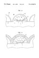
- FIG. 1 is a cross-sectional view showing the gate dielectric structure and the initial passivation anneal process operation
- FIG. 2 is a cross-sectional view showing the gate dielectric structure after a barrier film has been formed and sintered;
- FIG. 3 is a cross-sectional view showing the structure and the second “re-passivation” processing operation.
- FIG. 4 is a cross-sectional view showing the structure after a metal film has been added.
- the present invention provides a structure produced by an annealing sequence which effectively passivates trap sites in a dielectric film with deuterium.
- the processing sequence of the present invention occurs prior to the formation of metal films which will be formed into metal wiring patterns used in semiconductor integrated circuit devices.
- the process sequence of the present invention also utilizes a barrier material formed as a barrier film, and which is impervious to deuterium diffusion.
- the process sequence of the present invention also occurs sequentially following a high temperature source/drain anneal commonly performed upon integrated circuit devices.
- the present invention is not limited, however, to specific device structures. Further, the present invention is not intended to be used in conjunction with a specific barrier material, or at a specific processing point in the production of a semiconductor integrated circuit device.
- FIG. 1 is a cross-sectional view showing an exemplary embodiment of a structure being subjected to the first processing operation within the process sequence of the present invention.
- gate dielectric film 3 is formed over surface 9 of semiconductor substrate 1 .
- semiconductor substrate 1 may be a silicon wafer commonly used in the semiconductor manufacturing industry.
- gate dielectric film 3 may be a thermally grown oxide film. In alternative embodiments, however, the gate dielectric film 3 may be formed by other means common in the semiconductor manufacturing industry.
- gate dielectric film 3 is formed over channel region 7 of semiconductor substrate 1 , the region which will ultimately form a channel for a transistor device (not shown). For an MOS transistor device formed within semiconductor substrate 1 , source and drain regions will be subsequently formed lateral to channel region 7 within semiconductor substrate 1 .
- Interface region 4 is the portion of gate dielectric film 3 (hereinafter referred to as gate oxide film 3 , as in the preferred embodiment) closest to surface 9 of semiconductor substrate 1 .
- Interface region 4 is, generally speaking, a transition region between the amorphous oxide film 3 and the crystalline substrate 1 .
- Trap sites are formed within oxide film 3 , and especially within interface region 4 , upon formation of the oxide film. Trap sites may also be produced in response to processing operations subsequent to the initial formation of the film. Trap sites include impurities, incomplete bonds, dangling bonds and broken bonds in the oxide film 3 and within the interface region 4 .
- the present invention is directed to passivating these trap sites by complexing them with deuterium, so that trap sites are not available to be occupied by hot carriers which increases the charges trapped within the oxide film and can, in time, degrade device functionality.
- gate electrode 5 Disposed above gate oxide film 3 is gate electrode 5 .
- gate electrode 5 may be formed of a polysilicon film. Conventional methods for forming a polysilicon film on a substrate, then patterning the film to form a gate electrode, are common in the art. Any suitable method may be used.
- dielectric film 13 Disposed above and lateral to the gate structure, is dielectric film 13 .
- dielectric film 13 is a relatively thick (8,000 to 12,000 angstroms) undoped oxide film formed using plasma enhanced chemical vapor deposition (PECVD), or low pressure chemical vapor deposition (LPCVD) means. In alternative embodiments, other dielectric films may be used. Alternative means for forming dielectric film 13 over the substrate are common in the art, and any suitable method may be used.
- dielectric film 13 comprises a continuous film formed to cover all exposed surfaces of the substrate 1 .
- Contact holes 11 may be formed through dielectric film 13 for the purpose of providing contact to surface 9 of silicon substrate 1 .
- Conventional means for forming contact holes 11 include forming a photosensitive film (not shown) over dielectric film 13 , forming a pattern within the photosensitive film, then using the patterned photosensitive film as a mask to form a pattern within the dielectric film by means of plasma, or other etching techniques.
- contact holes 11 are shown in the exemplary embodiment, it is not significant that contact areas have been formed prior to the process of the present invention.
- Dielectric film 13 includes an outer, or leading surface 17 .
- the processing operation as shown in FIG. 1, is performed subsequent to any high temperature (800° C. to 1000° C.) source/drain anneal operations which may have been carried out on the device.
- FIG. 1 shows the initial processing operation in the passivation anneal process being carried out.
- Deuterium environment 10 includes deuterium gas and in an alternative embodiment may additionally include nitrogen gas mixed with the deuterium gas.
- deuterium passivation is carried out by heating at a temperature within the range of 400° C. to 700° C., for a time ranging from 30 minutes to 4 hours. In the preferred embodiment, an annealing temperature of greater than 450° C. may be used.
- Arrows 15 represent the diffusion path of deuterium molecules into and within the structure.
- the deuterium molecules first penetrate outer surface 17 of dielectric film 13 , then diffuse within the formed structure to passivate trap sites within dielectric film 13 as well as gate oxide film 3 including sites in interface region 4 .
- the presence of deuterium complexing with and thereby passivating trap sites is indicated by the symbol “D 2 ”.
- barrier layer 19 has been added to the structure shown in FIG. 1 .
- Barrier layer 19 is formed throughout the semiconductor device, and covers outer surface 17 of dielectric film 13 .
- barrier layer 19 will additionally cover regions of substrate surface 9 exposed through contact holes 11 .
- Conventional methods may be used to form the barrier film. These methods include sputter deposition, evaporation, and chemical vapor deposition. In the preferred embodiment, sputtering may be used.
- Barrier layer 19 may consist of a composite film of titanium/titanium nitride in an exemplary embodiment. In a preferred embodiment, a titanium nitride film is formed over a titanium film to form barrier layer 19 .
- a re-passivation annealing process shown in FIG. 3 is carried out to restore D 2 passivation of trap sites within gate oxide film 3 , including interface region 4 .
- an RTA or furnace anneal process is performed at a temperature below the temperature of the sintering process.
- the temperature of the re-passivation process may further be below the temperature of the initial D 2 passivation anneal step as carried out and described in conjunction with FIG. 1 .
- annealing gas 28 may be nitrogen.
- hydrogen or deuterium may additionally be used.
- the re-passivation process may be carried out in a conventional processing furnace, or using RTA techniques.
- the re-passivation process may be carried out in-situ with respect to the sintering process described in conjunction with FIG. 2 .
- process conditions may be varied and the substrate may continue to undergo processing without being removed from the furnace or RTA unit used to perform the high temperature sintering process.
- the re-passivation may constitute a separate process operation performed in a different processing unit.
- the re-passivation annealing time may range from 30 seconds to 5 minutes, most preferably 1 minute in the preferred embodiment. With respect to furnace processing, the re-passivation annealing time may range from 30 minutes to 60 minutes.
- the re-passivation annealing temperature may range from 400° C. to 500° C., but will be significantly less than the temperature used in the sintering operation. In the preferred embodiment, the re-passivation annealing process temperature will be equal to or less than the annealing temperature used in the initial passivation step as described in conjunction with FIG. 1 .
- the second annealing, or re-passivation process urges the diffusion (as shown by arrows 27 ) of deuterium within the encapsulated structure to produce a more uniform distribution of deuterium within the encapsulated structure.
- a significant amount of the trap sites within gate dielectric film 3 , and specifically within interface region 4 will once again be complexed by deuterium molecules represented by molecular symbol D 2 .
- the barrier film which is impervious to the deuterium molecules, prevents any deuterium molecules from diffusing out of the encapsulated structure during the re-passivation process.
- FIG. 4 shows a metal film 30 formed on the device after the passivation process sequence of the present invention. Since the deuterium molecules are encapsulated within the structure and beneath the barrier material, and since the introduction of the metal film precludes the subsequent use of processing steps utilizing temperatures greater than 400° C. to 450° C., it can be seen that the sites passivated with deuterium will remain passivated with the deuterium molecules. As such, the structure will remain resistant or immune to hot carrier aging effects. Therefore, the passivation anneal process which is commonly performed after a semiconductor integrated circuit device has been completely manufactured, may not be required to passivate the encapsulated sites.
- the present invention may be used to provide deuterium passivation to any oxide film used in the formation of a semiconductor device, and is not intended to be limited to the gate oxide film structure shown in the figures.
- alternative processing techniques may be used subsequently.
Abstract
Description
Claims (21)
Priority Applications (1)
| Application Number | Priority Date | Filing Date | Title |
|---|---|---|---|
| US09/378,856 US6187665B1 (en) | 1999-01-14 | 1999-08-23 | Process for deuterium passivation and hot carrier immunity |
Applications Claiming Priority (2)
| Application Number | Priority Date | Filing Date | Title |
|---|---|---|---|
| US11588199P | 1999-01-14 | 1999-01-14 | |
| US09/378,856 US6187665B1 (en) | 1999-01-14 | 1999-08-23 | Process for deuterium passivation and hot carrier immunity |
Publications (1)
| Publication Number | Publication Date |
|---|---|
| US6187665B1 true US6187665B1 (en) | 2001-02-13 |
Family
ID=26813677
Family Applications (1)
| Application Number | Title | Priority Date | Filing Date |
|---|---|---|---|
| US09/378,856 Expired - Lifetime US6187665B1 (en) | 1999-01-14 | 1999-08-23 | Process for deuterium passivation and hot carrier immunity |
Country Status (1)
| Country | Link |
|---|---|
| US (1) | US6187665B1 (en) |
Cited By (10)
| Publication number | Priority date | Publication date | Assignee | Title |
|---|---|---|---|---|
| US20020132493A1 (en) * | 2000-08-01 | 2002-09-19 | Victor Watt | Method to reduce charge interface traps and channel hot carrier degradation |
| US6521977B1 (en) * | 2000-01-21 | 2003-02-18 | International Business Machines Corporation | Deuterium reservoirs and ingress paths |
| US6605529B2 (en) * | 2001-05-11 | 2003-08-12 | Agere Systems Inc. | Method of creating hydrogen isotope reservoirs in a semiconductor device |
| US20040002205A1 (en) * | 2002-03-20 | 2004-01-01 | Jds Uniphase Corporation | Adherent all-gold electrode structure for lithium niobate based devices and the method of fabrication |
| US20060014332A1 (en) * | 2002-08-23 | 2006-01-19 | Chandra Mouli | SOI device having increased reliability and reduced free floating body effects |
| US20060148120A1 (en) * | 2005-01-04 | 2006-07-06 | Omnivision Technologies, Inc. | Deuterium alloy process for image sensors |
| US20080128833A1 (en) * | 2004-08-27 | 2008-06-05 | Takaaki Kawahara | High-Dielectric-Constant Film, Field-Effect Transistor and Semiconductor Integrated Circuit Device Using the Same, and Method for Producing High-Dielectric-Constant Film |
| US20080290399A1 (en) * | 2007-05-25 | 2008-11-27 | Cypress Semiconductor Corporation | Nonvolatile charge trap memory device having a deuterated layer in a multi-layer charge-trapping region |
| US20090082978A1 (en) * | 2007-09-20 | 2009-03-26 | Samsung Electronics Co., Ltd. | Method of detecting degradation of semiconductor devices and method of detecting degradation of integrated circuits |
| US9716153B2 (en) | 2007-05-25 | 2017-07-25 | Cypress Semiconductor Corporation | Nonvolatile charge trap memory device having a deuterated layer in a multi-layer charge-trapping region |
Citations (3)
| Publication number | Priority date | Publication date | Assignee | Title |
|---|---|---|---|---|
| WO1994009829A1 (en) * | 1992-11-02 | 1994-05-11 | Bracco International B.V. | Stable microbubble suspensions as enhancement agents for ultrasound echography |
| US5972765A (en) * | 1997-07-16 | 1999-10-26 | International Business Machines Corporation | Use of deuterated materials in semiconductor processing |
| US6025280A (en) * | 1997-04-28 | 2000-02-15 | Lucent Technologies Inc. | Use of SiD4 for deposition of ultra thin and controllable oxides |
-
1999
- 1999-08-23 US US09/378,856 patent/US6187665B1/en not_active Expired - Lifetime
Patent Citations (3)
| Publication number | Priority date | Publication date | Assignee | Title |
|---|---|---|---|---|
| WO1994009829A1 (en) * | 1992-11-02 | 1994-05-11 | Bracco International B.V. | Stable microbubble suspensions as enhancement agents for ultrasound echography |
| US6025280A (en) * | 1997-04-28 | 2000-02-15 | Lucent Technologies Inc. | Use of SiD4 for deposition of ultra thin and controllable oxides |
| US5972765A (en) * | 1997-07-16 | 1999-10-26 | International Business Machines Corporation | Use of deuterated materials in semiconductor processing |
Non-Patent Citations (5)
| Title |
|---|
| Ehrlich, Daniel J., "Emerging technologies for In Situ Processing", 1988 Martinus Nijhoff Publishers, p45-54, 1988. * |
| Ehrlich, Daniel, Emerging Technologies for In Situ Processing, pp 45-54, 1988. * |
| Lyding, J.W. "Reduction of hot eletron degradation in metal oxide semiconductor transistors by deuterium processing", Appl. Phys. Lett., 68 (18) Apr. 26, 1996, p2526-2528. * |
| Wolf, Stanley, Silicon Processing For The VLSI Era, vol. 2, p 188-189, 147-150, 1990. * |
| Wolf, Stanley, Silicon Processing for the VLSI Era, vol. 2, pp 188-189, 147-150, 1990. * |
Cited By (22)
| Publication number | Priority date | Publication date | Assignee | Title |
|---|---|---|---|---|
| US6521977B1 (en) * | 2000-01-21 | 2003-02-18 | International Business Machines Corporation | Deuterium reservoirs and ingress paths |
| US20030102529A1 (en) * | 2000-01-21 | 2003-06-05 | Jay Burnham | Deuterium reservoirs and ingress paths |
| US6770501B2 (en) * | 2000-01-21 | 2004-08-03 | International Business Machines Corporation | Deuterium reservoirs and ingress paths |
| US6797644B2 (en) * | 2000-08-01 | 2004-09-28 | Texas Instruments Incorporated | Method to reduce charge interface traps and channel hot carrier degradation |
| US20020132493A1 (en) * | 2000-08-01 | 2002-09-19 | Victor Watt | Method to reduce charge interface traps and channel hot carrier degradation |
| US6605529B2 (en) * | 2001-05-11 | 2003-08-12 | Agere Systems Inc. | Method of creating hydrogen isotope reservoirs in a semiconductor device |
| US20040002205A1 (en) * | 2002-03-20 | 2004-01-01 | Jds Uniphase Corporation | Adherent all-gold electrode structure for lithium niobate based devices and the method of fabrication |
| US6867134B2 (en) * | 2002-03-20 | 2005-03-15 | Jds Uniphase Corporation | Adherent all-gold electrode structure for lithium niobate based devices and the method of fabrication |
| US20060014332A1 (en) * | 2002-08-23 | 2006-01-19 | Chandra Mouli | SOI device having increased reliability and reduced free floating body effects |
| US7511341B2 (en) * | 2002-08-23 | 2009-03-31 | Micron Technology, Inc. | SOI device having increased reliability and reduced free floating body effects |
| US20080128833A1 (en) * | 2004-08-27 | 2008-06-05 | Takaaki Kawahara | High-Dielectric-Constant Film, Field-Effect Transistor and Semiconductor Integrated Circuit Device Using the Same, and Method for Producing High-Dielectric-Constant Film |
| US7253020B2 (en) * | 2005-01-04 | 2007-08-07 | Omnivision Technologies, Inc | Deuterium alloy process for image sensors |
| US20060148120A1 (en) * | 2005-01-04 | 2006-07-06 | Omnivision Technologies, Inc. | Deuterium alloy process for image sensors |
| US20080290399A1 (en) * | 2007-05-25 | 2008-11-27 | Cypress Semiconductor Corporation | Nonvolatile charge trap memory device having a deuterated layer in a multi-layer charge-trapping region |
| US8680601B2 (en) * | 2007-05-25 | 2014-03-25 | Cypress Semiconductor Corporation | Nonvolatile charge trap memory device having a deuterated layer in a multi-layer charge-trapping region |
| US9716153B2 (en) | 2007-05-25 | 2017-07-25 | Cypress Semiconductor Corporation | Nonvolatile charge trap memory device having a deuterated layer in a multi-layer charge-trapping region |
| US9741803B2 (en) | 2007-05-25 | 2017-08-22 | Cypress Semiconductor Corporation | Nonvolatile charge trap memory device having a deuterated layer in a multi-layer charge-trapping region |
| US10079314B2 (en) | 2007-05-25 | 2018-09-18 | Cypress Semiconductor Corporation | Nonvolatile charge trap memory device having a deuterated layer in a multi-layer charge-trapping region |
| US10263087B2 (en) | 2007-05-25 | 2019-04-16 | Cypress Semiconductor Corporation | Nonvolatile charge trap memory device having a deuterated layer in a multi-layer charge-trapping region |
| US20090082978A1 (en) * | 2007-09-20 | 2009-03-26 | Samsung Electronics Co., Ltd. | Method of detecting degradation of semiconductor devices and method of detecting degradation of integrated circuits |
| US8108159B2 (en) * | 2007-09-20 | 2012-01-31 | Samsung Electronics Co., Ltd. | Method of detecting degradation of semiconductor devices and method of detecting degradation of integrated circuits |
| KR101356425B1 (en) | 2007-09-20 | 2014-01-28 | 삼성전자주식회사 | Method for predicting degradation degree of MOS transistor and circuit character |
Similar Documents
| Publication | Publication Date | Title |
|---|---|---|
| KR100243286B1 (en) | Method for manufacturing a semiconductor device | |
| JP3209878B2 (en) | Semiconductor substrate provided with embedded insulating layer, method for improving electrical insulation of SIMOX semiconductor substrate, and method for manufacturing SIMOX semiconductor substrate | |
| US20080054371A1 (en) | Transistor having a locally provided metal silicide region in contact areas and a method of forming the transistor | |
| US6071784A (en) | Annealing of silicon oxynitride and silicon nitride films to eliminate high temperature charge loss | |
| FR2639762A1 (en) | PROCESS FOR PRODUCING ASYMMETRIC FIELD TRANSISTORS AND TRANSISTORS THEREOF | |
| JPH11204793A (en) | Electronic device gate oxide hardening method and semiconductor device | |
| US6187665B1 (en) | Process for deuterium passivation and hot carrier immunity | |
| KR19980080391A (en) | Semiconductor device having aluminum contact or via and manufacturing method thereof | |
| US5691234A (en) | Buried contact method to release plasma-induced charging damage on device | |
| US5705442A (en) | Optimized tungsten contact plug process via use of furnace annealed barrier layers | |
| JP4636414B2 (en) | Integrated circuit metal coating using titanium / aluminum alloy | |
| US3550256A (en) | Control of surface inversion of p- and n-type silicon using dense dielectrics | |
| US6329697B1 (en) | Semiconductor device including a charge-dispersing region and fabricating method thereof | |
| US6674151B1 (en) | Deuterium passivated semiconductor device having enhanced immunity to hot carrier effects | |
| US6232194B1 (en) | Silicon nitride capped poly resistor with SAC process | |
| US6576522B2 (en) | Methods for deuterium sintering | |
| JP3063898B2 (en) | Method for manufacturing semiconductor device | |
| EP1542289A1 (en) | Radiation resistant MOS structure | |
| KR20030079806A (en) | Method for manufacturing a semiconductor device having a layered gate electrode | |
| US6607993B1 (en) | Method using ultraviolet radiation for integrated circuit manufacturing | |
| US6169041B1 (en) | Method for enhancing the reliability of a dielectric layer of a semiconductor wafer | |
| JPH05136084A (en) | Method for forming metallization on surface of semiconductor device | |
| USH2128H1 (en) | Radiation hardened microcircuits | |
| JP3373480B2 (en) | Method of manufacturing read-only memory and method of storing wafer | |
| US20050233530A1 (en) | Enhanced gate structure |
Legal Events
| Date | Code | Title | Description |
|---|---|---|---|
| AS | Assignment |
Owner name: LUCENT TECHNOLOGIES, INC., NEW JERSEY Free format text: ASSIGNMENT OF ASSIGNORS INTEREST;ASSIGNORS:CHETLUR, SUNDAR S.;ROY, PRADIP K.;OATES, ANTHONY S.;AND OTHERS;REEL/FRAME:010195/0050 Effective date: 19990819 |
|
| STCF | Information on status: patent grant |
Free format text: PATENTED CASE |
|
| FEPP | Fee payment procedure |
Free format text: PAYOR NUMBER ASSIGNED (ORIGINAL EVENT CODE: ASPN); ENTITY STATUS OF PATENT OWNER: LARGE ENTITY |
|
| FPAY | Fee payment |
Year of fee payment: 4 |
|
| FPAY | Fee payment |
Year of fee payment: 8 |
|
| FPAY | Fee payment |
Year of fee payment: 12 |
|
| AS | Assignment |
Owner name: DEUTSCHE BANK AG NEW YORK BRANCH, AS COLLATERAL AG Free format text: PATENT SECURITY AGREEMENT;ASSIGNORS:LSI CORPORATION;AGERE SYSTEMS LLC;REEL/FRAME:032856/0031 Effective date: 20140506 |
|
| AS | Assignment |
Owner name: AVAGO TECHNOLOGIES GENERAL IP (SINGAPORE) PTE. LTD Free format text: ASSIGNMENT OF ASSIGNORS INTEREST;ASSIGNOR:AGERE SYSTEMS LLC;REEL/FRAME:035365/0634 Effective date: 20140804 |
|
| AS | Assignment |
Owner name: LSI CORPORATION, CALIFORNIA Free format text: TERMINATION AND RELEASE OF SECURITY INTEREST IN PATENT RIGHTS (RELEASES RF 032856-0031);ASSIGNOR:DEUTSCHE BANK AG NEW YORK BRANCH, AS COLLATERAL AGENT;REEL/FRAME:037684/0039 Effective date: 20160201 Owner name: AGERE SYSTEMS LLC, PENNSYLVANIA Free format text: TERMINATION AND RELEASE OF SECURITY INTEREST IN PATENT RIGHTS (RELEASES RF 032856-0031);ASSIGNOR:DEUTSCHE BANK AG NEW YORK BRANCH, AS COLLATERAL AGENT;REEL/FRAME:037684/0039 Effective date: 20160201 |
|
| AS | Assignment |
Owner name: BANK OF AMERICA, N.A., AS COLLATERAL AGENT, NORTH CAROLINA Free format text: PATENT SECURITY AGREEMENT;ASSIGNOR:AVAGO TECHNOLOGIES GENERAL IP (SINGAPORE) PTE. LTD.;REEL/FRAME:037808/0001 Effective date: 20160201 Owner name: BANK OF AMERICA, N.A., AS COLLATERAL AGENT, NORTH Free format text: PATENT SECURITY AGREEMENT;ASSIGNOR:AVAGO TECHNOLOGIES GENERAL IP (SINGAPORE) PTE. LTD.;REEL/FRAME:037808/0001 Effective date: 20160201 |
|
| AS | Assignment |
Owner name: AVAGO TECHNOLOGIES GENERAL IP (SINGAPORE) PTE. LTD., SINGAPORE Free format text: TERMINATION AND RELEASE OF SECURITY INTEREST IN PATENTS;ASSIGNOR:BANK OF AMERICA, N.A., AS COLLATERAL AGENT;REEL/FRAME:041710/0001 Effective date: 20170119 Owner name: AVAGO TECHNOLOGIES GENERAL IP (SINGAPORE) PTE. LTD Free format text: TERMINATION AND RELEASE OF SECURITY INTEREST IN PATENTS;ASSIGNOR:BANK OF AMERICA, N.A., AS COLLATERAL AGENT;REEL/FRAME:041710/0001 Effective date: 20170119 |
|
| AS | Assignment |
Owner name: BELL SEMICONDUCTOR, LLC, ILLINOIS Free format text: ASSIGNMENT OF ASSIGNORS INTEREST;ASSIGNORS:AVAGO TECHNOLOGIES GENERAL IP (SINGAPORE) PTE. LTD.;BROADCOM CORPORATION;REEL/FRAME:044886/0001 Effective date: 20171208 |
|
| AS | Assignment |
Owner name: CORTLAND CAPITAL MARKET SERVICES LLC, AS COLLATERA Free format text: SECURITY INTEREST;ASSIGNORS:HILCO PATENT ACQUISITION 56, LLC;BELL SEMICONDUCTOR, LLC;BELL NORTHERN RESEARCH, LLC;REEL/FRAME:045216/0020 Effective date: 20180124 |
|
| AS | Assignment |
Owner name: BELL NORTHERN RESEARCH, LLC, ILLINOIS Free format text: SECURITY INTEREST;ASSIGNOR:CORTLAND CAPITAL MARKET SERVICES LLC;REEL/FRAME:060885/0001 Effective date: 20220401 Owner name: BELL SEMICONDUCTOR, LLC, ILLINOIS Free format text: SECURITY INTEREST;ASSIGNOR:CORTLAND CAPITAL MARKET SERVICES LLC;REEL/FRAME:060885/0001 Effective date: 20220401 Owner name: HILCO PATENT ACQUISITION 56, LLC, ILLINOIS Free format text: SECURITY INTEREST;ASSIGNOR:CORTLAND CAPITAL MARKET SERVICES LLC;REEL/FRAME:060885/0001 Effective date: 20220401 |