US6186610B1 - Imaging apparatus capable of suppressing inadvertent ejection of a satellite ink droplet therefrom and method of assembling same - Google Patents
Imaging apparatus capable of suppressing inadvertent ejection of a satellite ink droplet therefrom and method of assembling same Download PDFInfo
- Publication number
- US6186610B1 US6186610B1 US09/157,455 US15745598A US6186610B1 US 6186610 B1 US6186610 B1 US 6186610B1 US 15745598 A US15745598 A US 15745598A US 6186610 B1 US6186610 B1 US 6186610B1
- Authority
- US
- United States
- Prior art keywords
- transducer
- sensor
- pressure wave
- reflected portion
- operating mode
- Prior art date
- Legal status (The legal status is an assumption and is not a legal conclusion. Google has not performed a legal analysis and makes no representation as to the accuracy of the status listed.)
- Expired - Lifetime
Links
Images


Classifications
-
- B—PERFORMING OPERATIONS; TRANSPORTING
- B41—PRINTING; LINING MACHINES; TYPEWRITERS; STAMPS
- B41J—TYPEWRITERS; SELECTIVE PRINTING MECHANISMS, i.e. MECHANISMS PRINTING OTHERWISE THAN FROM A FORME; CORRECTION OF TYPOGRAPHICAL ERRORS
- B41J2/00—Typewriters or selective printing mechanisms characterised by the printing or marking process for which they are designed
- B41J2/005—Typewriters or selective printing mechanisms characterised by the printing or marking process for which they are designed characterised by bringing liquid or particles selectively into contact with a printing material
- B41J2/01—Ink jet
- B41J2/015—Ink jet characterised by the jet generation process
- B41J2/04—Ink jet characterised by the jet generation process generating single droplets or particles on demand
- B41J2/045—Ink jet characterised by the jet generation process generating single droplets or particles on demand by pressure, e.g. electromechanical transducers
- B41J2/04501—Control methods or devices therefor, e.g. driver circuits, control circuits
- B41J2/04516—Control methods or devices therefor, e.g. driver circuits, control circuits preventing formation of satellite drops
-
- B—PERFORMING OPERATIONS; TRANSPORTING
- B41—PRINTING; LINING MACHINES; TYPEWRITERS; STAMPS
- B41J—TYPEWRITERS; SELECTIVE PRINTING MECHANISMS, i.e. MECHANISMS PRINTING OTHERWISE THAN FROM A FORME; CORRECTION OF TYPOGRAPHICAL ERRORS
- B41J2/00—Typewriters or selective printing mechanisms characterised by the printing or marking process for which they are designed
- B41J2/005—Typewriters or selective printing mechanisms characterised by the printing or marking process for which they are designed characterised by bringing liquid or particles selectively into contact with a printing material
- B41J2/01—Ink jet
- B41J2/015—Ink jet characterised by the jet generation process
- B41J2/04—Ink jet characterised by the jet generation process generating single droplets or particles on demand
- B41J2/045—Ink jet characterised by the jet generation process generating single droplets or particles on demand by pressure, e.g. electromechanical transducers
- B41J2/04501—Control methods or devices therefor, e.g. driver circuits, control circuits
- B41J2/04551—Control methods or devices therefor, e.g. driver circuits, control circuits using several operating modes
-
- B—PERFORMING OPERATIONS; TRANSPORTING
- B41—PRINTING; LINING MACHINES; TYPEWRITERS; STAMPS
- B41J—TYPEWRITERS; SELECTIVE PRINTING MECHANISMS, i.e. MECHANISMS PRINTING OTHERWISE THAN FROM A FORME; CORRECTION OF TYPOGRAPHICAL ERRORS
- B41J2/00—Typewriters or selective printing mechanisms characterised by the printing or marking process for which they are designed
- B41J2/005—Typewriters or selective printing mechanisms characterised by the printing or marking process for which they are designed characterised by bringing liquid or particles selectively into contact with a printing material
- B41J2/01—Ink jet
- B41J2/015—Ink jet characterised by the jet generation process
- B41J2/04—Ink jet characterised by the jet generation process generating single droplets or particles on demand
- B41J2/045—Ink jet characterised by the jet generation process generating single droplets or particles on demand by pressure, e.g. electromechanical transducers
- B41J2/04501—Control methods or devices therefor, e.g. driver circuits, control circuits
- B41J2/04581—Control methods or devices therefor, e.g. driver circuits, control circuits controlling heads based on piezoelectric elements
-
- B—PERFORMING OPERATIONS; TRANSPORTING
- B41—PRINTING; LINING MACHINES; TYPEWRITERS; STAMPS
- B41J—TYPEWRITERS; SELECTIVE PRINTING MECHANISMS, i.e. MECHANISMS PRINTING OTHERWISE THAN FROM A FORME; CORRECTION OF TYPOGRAPHICAL ERRORS
- B41J2/00—Typewriters or selective printing mechanisms characterised by the printing or marking process for which they are designed
- B41J2/005—Typewriters or selective printing mechanisms characterised by the printing or marking process for which they are designed characterised by bringing liquid or particles selectively into contact with a printing material
- B41J2/01—Ink jet
- B41J2/015—Ink jet characterised by the jet generation process
- B41J2/04—Ink jet characterised by the jet generation process generating single droplets or particles on demand
- B41J2/045—Ink jet characterised by the jet generation process generating single droplets or particles on demand by pressure, e.g. electromechanical transducers
- B41J2/04501—Control methods or devices therefor, e.g. driver circuits, control circuits
- B41J2/04588—Control methods or devices therefor, e.g. driver circuits, control circuits using a specific waveform
-
- B—PERFORMING OPERATIONS; TRANSPORTING
- B41—PRINTING; LINING MACHINES; TYPEWRITERS; STAMPS
- B41J—TYPEWRITERS; SELECTIVE PRINTING MECHANISMS, i.e. MECHANISMS PRINTING OTHERWISE THAN FROM A FORME; CORRECTION OF TYPOGRAPHICAL ERRORS
- B41J2/00—Typewriters or selective printing mechanisms characterised by the printing or marking process for which they are designed
- B41J2/005—Typewriters or selective printing mechanisms characterised by the printing or marking process for which they are designed characterised by bringing liquid or particles selectively into contact with a printing material
- B41J2/01—Ink jet
- B41J2/015—Ink jet characterised by the jet generation process
- B41J2/04—Ink jet characterised by the jet generation process generating single droplets or particles on demand
- B41J2/045—Ink jet characterised by the jet generation process generating single droplets or particles on demand by pressure, e.g. electromechanical transducers
- B41J2/04501—Control methods or devices therefor, e.g. driver circuits, control circuits
- B41J2/04596—Non-ejecting pulses
-
- B—PERFORMING OPERATIONS; TRANSPORTING
- B41—PRINTING; LINING MACHINES; TYPEWRITERS; STAMPS
- B41J—TYPEWRITERS; SELECTIVE PRINTING MECHANISMS, i.e. MECHANISMS PRINTING OTHERWISE THAN FROM A FORME; CORRECTION OF TYPOGRAPHICAL ERRORS
- B41J2/00—Typewriters or selective printing mechanisms characterised by the printing or marking process for which they are designed
- B41J2/005—Typewriters or selective printing mechanisms characterised by the printing or marking process for which they are designed characterised by bringing liquid or particles selectively into contact with a printing material
- B41J2/01—Ink jet
- B41J2/015—Ink jet characterised by the jet generation process
- B41J2/04—Ink jet characterised by the jet generation process generating single droplets or particles on demand
- B41J2/045—Ink jet characterised by the jet generation process generating single droplets or particles on demand by pressure, e.g. electromechanical transducers
- B41J2/055—Devices for absorbing or preventing back-pressure
-
- B—PERFORMING OPERATIONS; TRANSPORTING
- B41—PRINTING; LINING MACHINES; TYPEWRITERS; STAMPS
- B41J—TYPEWRITERS; SELECTIVE PRINTING MECHANISMS, i.e. MECHANISMS PRINTING OTHERWISE THAN FROM A FORME; CORRECTION OF TYPOGRAPHICAL ERRORS
- B41J2/00—Typewriters or selective printing mechanisms characterised by the printing or marking process for which they are designed
- B41J2/005—Typewriters or selective printing mechanisms characterised by the printing or marking process for which they are designed characterised by bringing liquid or particles selectively into contact with a printing material
- B41J2/01—Ink jet
- B41J2/135—Nozzles
- B41J2/14—Structure thereof only for on-demand ink jet heads
- B41J2002/14354—Sensor in each pressure chamber
-
- B—PERFORMING OPERATIONS; TRANSPORTING
- B41—PRINTING; LINING MACHINES; TYPEWRITERS; STAMPS
- B41J—TYPEWRITERS; SELECTIVE PRINTING MECHANISMS, i.e. MECHANISMS PRINTING OTHERWISE THAN FROM A FORME; CORRECTION OF TYPOGRAPHICAL ERRORS
- B41J2202/00—Embodiments of or processes related to ink-jet or thermal heads
- B41J2202/01—Embodiments of or processes related to ink-jet heads
- B41J2202/10—Finger type piezoelectric elements
Definitions
- the present invention relates to imaging apparatus and methods and more particularly relates to an imaging apparatus capable of suppressing inadvertent ejection of a satellite ink droplet therefrom and method of assembling same.
- An imaging apparatus such as an ink jet printer, produces images on a receiver medium by ejecting ink droplets onto the receiver medium in an image-wise fashion.
- the advantages of non-impact, low-noise, low energy use, and low cost operation in addition to the ability of the printer to print on plain paper are largely responsible for the wide acceptance of ink jet printers in the marketplace.
- the ink jet printer of the Wen disclosure includes a piezoelectric print head capable of varying direction of an ink droplet to be ejected from the print head.
- a pair of sidewalls belonging to the print head define an ink channel therebetween containing ink.
- the print head includes addressable electrodes attached to the side walls for actuating (i.e., moving) the sidewalls, so that the ink droplet is ejected from the ink channel.
- a pulse generator applies time and amplitude varying electrical pulses to the addressable electrodes for actuating the sidewalls.
- a pressure wave is established in the ink contained in the channel.
- this pressure wave squeezes a portion of the ink in the form of the ink droplet out the channel.
- the pressure wave impacts the sidewalls defining the channel and is reflected therefrom.
- the pressure wave reflected from the sidewalls establishes a reflected pressure wave in the channel, this reflected pressure wave being defined herein as a “reflected portion” of the incident pressure wave.
- the reflected portion dies-out before each successive actuation of the sidewalls.
- the reflected portion of the pressure wave may be of amplitude sufficient to inadvertently eject an unintended so-called “satellite droplet” that follows ejection of the intended ink droplet but that occurs before the reflected portion dies-out.
- Satellite ink droplet formation is undesirable because such inadvertent satellite ink droplet formation interferes with precise ejection of ink droplets from the ink channels, which leads to ink droplet placement errors.
- These ink droplet placement errors in turn produce image artifacts such as banding, reduced image sharpness, extraneous ink spots, ink coalescence and color bleeding.
- a problem in the art is satellite ink droplet formation leading to ink droplet placement errors.
- printer speed is selected such that electrical pulses are applied to the addressable electrodes at intervals after each reflected portion dies-out.
- Such delayed printer operation is required in order to avoid the unintended reflected portion interfering with the intended pressure wave. Otherwise allowing the reflected portion to interfere with the intended pressure wave may result in the aforementioned ink droplet placement errors.
- operating the printer in this manner reduces printing speed because ejection of ink droplets must await the cessation of the reflected portion of the pressure wave. Therefore, quite apart from the aforementioned problem of satellite droplet formation, another problem in the art is reduced printer speed due to presence of the reflected portion of the intended pressure wave.
- An object of the present invention is to provide an imaging apparatus capable of suppressing inadvertent ejection of a satellite ink droplet therefrom while maintaining printing speed, and method of assembling the apparatus.
- the invention resides in an imaging apparatus, comprising a transducer defining a chamber therein, said transducer capable of inducing a first pressure wave in the chamber, the first pressure wave having a reflected portion; and a deflectable sensor coupled to the chamber for sensing the reflected portion and connected to said transducer for actuating said transducer in response to the reflected portion sensed thereby, so that said transducer actuates to induce a second pressure wave in the chamber damping the reflected portion, said sensor capable of deflecting as said sensor senses the reflected portion.
- an imaging apparatus with pressure sensor, is provided that is capable of suppressing inadvertent ejection of a satellite ink droplet from an ink body residing in the imaging apparatus.
- the imaging apparatus comprises a print head defining a chamber having the ink body disposed therein.
- a transducer e.g., a piezoelectric transducer
- a transducer is in fluid communication with the ink body for inducing a first pressure wave in the ink body, which first pressure wave has a reflected portion of a first amplitude and a first phase sufficient to inadvertently eject satellite droplets.
- a waveform generator is connected to the transducer for supplying a first voltage waveform to the transducer, so that the transducer induces the first pressure wave in the ink body.
- a sensor is in fluid communication with the ink body for sensing the reflected portion of the first pressure wave and for generating a second voltage waveform in response to the reflected portion sensed by the sensor.
- a feedback circuit is connected to the sensor for receiving the second voltage waveform generated by the sensor. The feedback circuit converts the second voltage waveform to a third voltage waveform. The amplitude and phase of the third voltage waveform are chosen by the feedback circuit to rapidly drive the reflected portion and thus the second voltage waveform to zero.
- the third voltage waveform is transmitted to the transducer, so that the transducer controllably actuates in response to the third voltage waveform supplied thereto.
- This third voltage waveform induces a second pressure wave in the ink body.
- the second pressure wave has a second amplitude and a second phase which damps the amplitude of the reflected portion of the first pressure wave in order to suppress inadvertent ejection of satellite ink droplets. This is so because the amplitude and phase of the third voltage waveform are chosen by the feedback circuit to rapidly drive the reflected portion and thus the second voltage waveform to zero, as previously mentioned.
- the imaging apparatus further comprises a switch capable of switching between a first operating mode and a second operating mode.
- the switch When the switch switches to the first operating mode, the switch connects the waveform generator to the transducer for actuating the transducer in order to produce the first pressure wave in the chamber.
- the switch When the switch switches to the second operating mode, the switch connects the feedback circuit to the sensor and transducer for sensing the reflected portion of the first pressure wave and for damping the reflected portion in the manner mentioned hereinabove.
- a feature of the present invention is the provision of a sensor coupled to the chamber for sensing the reflected portion of the first pressure wave.
- Another feature of the present invention is the provision of a feedback circuit connected to the sensor for controllably applying the second pressure wave to the ink body, such that the second pressure wave damps the reflected portion of the first pressure wave.
- An advantage of the present invention is that satellite ink droplet formation is inhibited.
- Another advantage of the present invention is that printing speed is maintained as satelite ink droplet formation is inhibited.
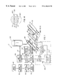
- FIG. 1 shows an imaging apparatus comprising a print head
- FIG. 1A is a fragmentation view in elevation of the print head
- FIG. 2 is a fragmentation view in perspective of the print head, this view showing a front side of the print head and also showing a first embodiment pressure sensor in communication with ink chambers formed in the print head;
- FIG. 3 is a fragmentation view in perspective of the print head, this view showing a rear side of the print head with an attached manifold;
- FIG. 4 is a fragmentation view in perspective of the print head, the view showing the rear side of the print head without the attached manifold;
- FIG. 5 is a fragmentation view in horizontal section of the print head
- FIG. 6 shows a graph of a first voltage waveform applied to the print head
- FIG. 7 shows a graph of a first pressure wave produced by the first voltage waveform, the first pressure wave having a reflected portion
- FIG. 8 shows a graph including a second voltage waveform produced in response to a sensor sensing the reflected portion of the first pressure wave
- FIG. 9 shows a graph of a third voltage waveform applied to the print head
- FIG. 10 shows a graph including a second pressure wave produced by the third voltage waveform for damping the reflected portion of the first pressure wave
- FIG. 11 is a fragmentation view in perspective of the print head, the view also showing a second embodiment pressure sensor in communication with the ink chambers;
- FIG. 12 is an enlarged fragmentation view in elevation of the print head and second embodiment pressure sensor
- FIG. 13 is a fragmentation view in perspective of the print head, this view showing a third embodiment pressure sensor in communication with the ink chambers;
- FIG. 14 is a fragmentation view in perspective of the print head, this view showing a fourth embodiment pressure sensor in communication with the ink chambers;
- FIG. 15 is a fragmentation view in perspective of the print head, this view showing a fifth embodiment pressure sensor in communication with the ink chambers;
- FIG. 16 is a fragmentation view in perspective of the print head, this view showing a sixth embodiment pressure sensor in communication with the ink chambers;
- FIG. 17 is a fragmentation view in perspective of the print head, this view showing a seventh embodiment pressure sensor in communication with the ink chambers.
- FIGS. 1 and 1A there is shown the subject matter of the present invention, which is an imaging apparatus, generally referred to as 10 , for ejecting an ink droplet 20 from a print head 25 toward a receiver 30 .
- receiver 30 may be a reflective-type (e.g., paper) or transmissive-type (e.g., transparency) receiver.
- apparatus 10 is capable of ejecting droplet 20
- apparatus 10 is also capable of inhibiting inadvertent ejection of a so-called “satellite ink droplet” 22 , as described in detail hereinbelow.
- imaging apparatus 10 which is preferably an ink jet printer, comprises an image source 40 , which may be raster image data from a scanner or computer, or outline image data in the form of a PDL (Page Description Language) or other form of digital image representation.
- image data is transmitted to an image processor 50 connected to image source 40 .
- Image processor 50 converts the image data to a pixel-mapped page image.
- Image processor 50 may be a raster image processor in the case of PDL image data to be converted, or a pixel image processor in the case of raster image data to be converted. In any case, image processor 50 transmits continuous tone data to a digital halftoning unit 60 connected to image processor 50 .
- Halftoning unit 60 halftones the continuous tone data produced by image processor 50 and produces halftoned bitmap image data that is stored in an image memory 70 , which may be a full-page memory or a band memory depending on the configuration of imaging apparatus 10 .
- a waveform generator 80 connected to image memory 70 reads data from image memory 70 and applies time and amplitude varying electrical stimuli, through an amplifier 85 , to an electrical actuator (i.e., an electrode), as described more fully hereinbelow.
- receiver 30 is moved relative to print head 25 by means of a transport mechanism 90 , such as rollers 100 , which are electronically controlled by a transport control system 10 .
- Transport control system 110 in turn is controlled by a suitable controller 120 .
- a suitable controller 120 it may be appreciated that various mechanical configurations for transport control system 110 are possible. For example, in the case of pagewidth print heads, it is convenient to move receiver 30 past a stationary print head 25 . On the other hand, in the case of scanning-type printing systems, it is more convenient to move print head 25 along one axis (i.e., a sub-scanning direction) and receiver 30 along an orthogonal axis (i.e., a main scanning direction), in a relative raster motion.
- a sub-scanning direction i.e., a sub-scanning direction
- receiver 30 along an orthogonal axis (i.e., a main scanning direction), in a relative raster motion.
- controller 120 may be connected to an ink pressure regulator 130 for controlling regulator 130 .
- Regulator 130 if present, is capable of regulating pressure in an ink reservoir 140 .
- Ink reservoir 140 is connected, such as by means of a conduit 150 , to print head 25 for supplying liquid ink to print head 25 .
- ink is preferably distributed to a back surface of print head 25 by a manifold 155 belonging to print head 25 .
- Manifold 155 includes a plurality of openings 157 for reasons disclosed hereinbelow.
- print head 25 comprises a generally cuboid-shaped preferably one-piece transducer 160 formed of a piezoelectric material, such as lead zirconate titanate (PZT), which is responsive to electrical stimuli.
- PZT lead zirconate titanate
- Cut into transducer 160 are a plurality of elongate ink chambers 170 capable of accepting ink supplied thereinto from manifold 155 through the previously mentioned orifices 157 .
- Each opening 157 is aligned with its respective channel 170 .
- Each of the chambers 170 has a chamber outlet 171 at an end 177 thereof and an open side 173 extending the length of chamber 170 .
- Ink chambers 170 are covered at outlets 171 by a nozzle plate 174 having a plurality of colinearly aligned orifices 175 that are themselves aligned with respective ones of chamber outlets 171 , so that ink droplets 20 are ejected from chamber outlets 171 and through their respective orifices 175 and thereafter along a trajectory normal to nozzle plate 174 .
- Nozzle plate 174 itself, is attached to a front side of transducer 160 .
- Ink manifold 155 which is attached to a rear side of transducer 160 , has ink therein for supplying the ink to chambers 175 .
- a top cover plate shown in phantom, caps chambers 170 along open side 173 .
- ink from reservoir 140 is controllably supplied to manifold 155 by means of conduit 150 and thence to each chamber 175 .
- transducer 160 includes a first side wall 180 and a second side wall 190 defining chamber 170 therebetween, which chamber 170 is adapted to receive an ink body 200 therein. Moreover, cut into transducer 160 between adjacent chambers 170 and extending parallel thereto may be a cutout 205 separating chambers 170 for reducing mechanical and hydraulic coupling (i.e., “cross-talk”) between chambers 170 .
- Each first side wall 180 has an outside surface 185 facing cut-out 205 and each second side wall 190 has an outside surface 195 also facing cut-out 205 .
- Transducer 160 also includes a base portion 210 interconnecting first side wall 180 and second side wall 190 , so as to form a generally U-shaped structure of the piezoelectric material. Upper-most surfaces (as shown) of first wall 180 and second wall 190 together define a top surface 220 of transducer 160 . Base portion 210 defines a bottom surface 230 of transducer 160 (as shown).
- an addressable electrode actuator layer 240 is deposited on sidewalls 180 / 190 . In this configuration of addressable electrode layer 240 , an electrical field (not shown) is established in a predetermined orientation to actuate sidewalls 180 / 190 .
- addressable electrode layer 240 is connected to the previously mentioned waveform generator 80 via amplifier 85 . In this regard, waveform generator 80 supplies amplified electrical stimuli to each of the portions of addressable electrode layer 240 via an electrical conducting terminal 260 .
- a common electrode layer 270 coats each chamber 170 and also extends therefrom along top surface 220 .
- Common electrode layer 270 is preferably connected to a ground electric potential, as at a point 280 .
- waveform generator 80 supplies electrical stimuli to addressable electrode actuator layer 240
- the previously mentioned electric field (not shown) is established between addressable electrode actuator layer 240 and common electrode layer 270 .
- This electric field in piezoelectric sidewalls 180 / 190 deforms and inwardly moves sidewalls 180 / 190 .
- ink droplet 20 is ejected from chamber 170 in order to form an image 285 (see FIG. 1) on receiver 30 .
- first electrical waveform for inducing a first pressure wave, generally referred to as 300 , in ink body 200 .
- First pressure wave 300 which may be oscillating in nature (as shown), is induced in ink body 200 in order to squeeze ink droplet 20 from ink body 200 and thereby eject ink droplet 20 from chamber 170 .
- waveform generator 80 supplies first voltage waveform 290 through amplifier 85 to addressable electrode layer 240 , via terminal 260 , in order to electrically stimulate pair of sidewalls 180 / 190 .
- Sidewalls 180 / 190 deform as sidewalls 180 / 190 are electrically stimulated.
- First electrical waveform 290 has a voltage amplitude V 1 and a time duration ⁇ t v1 .
- first pressure wave 300 is induced in ink body 200 .
- This first pressure wave 300 has a first amplitude P 1 and a first time duration ⁇ t P1 .
- first pressure wave 300 is reflected from sidewalls 180 / 190 and from nozzle plate 174 and gasket 158 .
- first pressure wave 300 forms an undesirable reflected portion 310 of first pressure wave 300 .
- Reflected portion 310 may be oscillating in nature (as shown).
- reflected portion 310 When present, reflected portion 310 will have a maximum pressure amplitude P r lower than amplitude P 1 , to be followed by successively lower amplitudes until reflected portion 310 dies-out, as generally shown at point 315 .
- reflected portion 310 of first pressure wave 310 may have amplitudes sufficient to inadvertently eject so-called “satellite” droplet 22 following ejection of the intended ink droplet 20 .
- Satellite ink droplet formation is undesirable because such satellite ink droplet formation interferes with precise ejection of ink droplets 20 from ink chambers 170 , which in turn leads to ink droplet placement errors.
- reflected portion 310 of first pressure wave 300 eventually dies-out.
- printer speed must be reduced in order that waveform 290 be applied to addressable electrode 240 at intervals after each reflected portion 310 dies-out.
- the invention suppresses formation of reflected portion 310 so that printer speed is increased.
- a first embodiment pressure sensor 320 is coupled to each chamber 170 .
- First embodiment sensor 320 may be a relatively thin one-piece piezoelectric sensor wafer 325 spanning all chambers 170 .
- sensor wafer 325 is in fluid communication with each ink body 200 .
- the purpose of wafer 325 is to sense pressure changes occurring in any chamber 170 by sensing presence of reflected portion 310 of first pressure wave 300 . It may be understood from the teachings herein, that reflected portion 310 gives rise to pressure changes in chamber 170 .
- These pressure changes deflect piezoelectric wafer 325 .
- second voltage waveform 330 has an amplitude V 2 and a time duration ⁇ t V2 .
- a suitable wafer 325 usable with the invention may be of a type disclosed in an article titled “Designing, Realization And Characterization Of A Novel Capacative Pressure/Flow Sensor” authored by R. E. Oosterbroek and published in the Proceedings, IEEE Transducers Conference, 1997, pages 151-154.
- a feedback circuit 340 is connected to wafer 325 , such as by an electrode 345 deposited thereon, for receiving second voltage waveform 330 .
- Feedback circuit 340 is capable of converting second voltage waveform 330 to a third voltage waveform 350 to be applied through amplifier 85 to addressable electrode layer 240 in order to damp reflected portion 310 of first pressure wave 300 .
- third voltage waveform 350 acts as a transducer drive signal. More specifically, feedback circuit 340 calculates third voltage waveform 350 based on second voltage waveform 330 , which is received from wafer 325 , as described in detail presently.
- third voltage waveform 350 is generated by feedback circuit 340 so as to have an amplitude V 3 and a time duration ⁇ t V3 to drive the input second voltage waveform 330 to zero, and thus dampen the reflected portion 310 of first pressure wave 300 .
- Feedback circuit 340 is connected to amplifier 85 and transmits this third voltage waveform 350 to transducer 160 via amplifier 85 . That is, amplifier 85 receives third voltage waveform 350 transmitted by feedback circuit 340 and supplies the amplified third voltage waveform 350 to addressable electrode actuator layer 240 .
- Addressable electrode layer 240 receives third voltage waveform 350 so as to deform sidewalls 180 / 190 belonging to transducer 160 .
- Second pressure wave 360 has an amplitude P 2 and a time duration ⁇ t P2 .
- second pressure wave 360 has amplitude P 2 and a phase (as shown) that effectively damps reflected portion 310 , so that satellite droplets 22 are not formed and so that printing speed is increased.
- wafer 325 and feedback circuit 340 are arranged so as to define a feed-back loop 365 , for reasons disclosed hereinbelow.
- feedback circuit 340 calculates third voltage waveform 350 based on second voltage waveform 310 that is received from wafer 325 , as previously mentioned.
- the amplified third voltage waveform 350 that is supplied to sidewalls 180 / 190 damps reflected portion 310 .
- wafer 325 is first calibrated in “open-loop mode”.
- Equation (1) a known voltage V 3 is applied through amplifier 85 to transducer 160 , which will produce a resulting pressure P in the ink chamber 170 , which in turn will cause sensor 320 to produce a voltage V sense , the value of which depends on the magnitude of P. This is then repeated for a plurality of applied voltages V 3 in order to determine a quantitative relation between V 3 and V sense , as in Equation (1):
- V sense G*V 3 Equation (1)
- V 3 ⁇ ( 1/ G )* V 2 Equation (2)
- the third voltage output signal V 3 is chosen in order to cause a second pressure wave 360 in the ink chamber 170 which will exactly cancel the reflected portion 310 that led to the sensor signal V 2 .
- V 3 will quickly cause the sensor signal to become zero, as the pressure waves in chamber 170 are quickly damped-out.
- the circuit which implements Equation (2) may easily include an inverter, followed by a multiplier.
- Equation (2) the calibration relation, Equation (2), between V 3 and V sense alternatively may be stored in a look-up table (LUT), as well.
- LUT look-up table
- the operation of forming the output signal V 3 may also be accomplished by digital signal processing circuitry embodied in a micro-controller which is in communication with the above mentioned LUT.
- switch 370 is capable of switching between a first operating mode and a second operating mode.
- switch 370 connects waveform generator 80 to amplifier 85 and therefore to transducer 160 .
- waveform generator 80 drives amplifier 85 and transducer 160 to eject ink droplet 20 .
- switch 370 connects transducer 160 and amplifier 85 to feedback circuit 340 , which belongs to feedback loop 365 . Consequently, in the second operating mode of switch 370 , sensor 320 senses presence of reflected portion 310 of first pressure wave 300 .
- a suitable switch 370 may be a so-called “T-switch” which is available from Siliconix Corporation located in Santa Clara, Calif.
- a second embodiment sensor 320 is there shown comprising a layered wafer 380 .
- Layered wafer 380 includes a flexible substrate 390 to which a piezoelectric layer 400 is attached.
- Layer 400 serves the same function as wafer 325 .
- An advantage of this second embodiment of the invention is that the piezoelectric material need not be in direct contact with ink in chamber 170 , thus making chamber 170 easier to passivate against various ink types.
- FIG. 13 shows a third embodiment sensor 320 , wherein there are a plurality of piezoelectric sensor strips 410 in fluid communication with respective ones of ink bodies 200 .
- each sensor strip 410 extends along its respective open side 173 of chamber 170 , such that sensor strip 410 caps chamber 170 .
- An advantage of this third embodiment of the invention is that pressure changes in each chamber 170 is sensed by corresponding sensor strips 410 .
- third voltage V 3 can now be applied to sidewalls 180 / 190 defining individual chambers 170 for damping reflected portion 310 in individual chambers 170 .
- This is a useful feature of the invention because pressure amplitude P r of reflected portion 310 may itself be different in different chambers 170 .
- the invention accommodates variability in pressure P r among individual chambers 170 .
- FIG. 14 shows a fourth embodiment sensor 320 .
- a plurality of elongate piezoelectric sensor segments 420 a and 420 b line each chamber 170 and are in fluid communication with ink bodies 200 .
- Sensor segments 420 a/b extend longitudinally along outside surface 185 of first sidewall 180 and outside surface 195 of second sidewall 190 .
- Adjacent sensor segments 420 a and 420 b may be colinearly aligned (as shown) and separated by a gap 430 .
- An advantage of this configuration of the invention is that pressure of reflected portion 310 of first pressure wave 300 as a function of time is obtainable as reflected portion 310 propagates in chamber 170 .
- a fifth embodiment sensor 320 is attached directly to ink manifold gasket 158 that is attached directly to the rear of chambers 170 .
- Sensor 320 spans all chambers 170 of printhead 25 .
- the advantage of fifth embodiment sensor 320 is that sensor 320 is directly attached to the back of the chamber, and therefore detects both the amplitude of the pressure wave 300 as well as the pressure as a function of time.
- FIG. 16 shows a sixth embodiment sensor 320 , wherein there are a plurality of piezoelectric sensors in fluid communications with respective ink bodies 200 .
- An advantage of this sixth embodiment sensor 320 is that pressure changes in each chamber 170 are sensed by respective sensors 320 . This is a useful feature of the invention because pressure amplitude P r of reflected portion 310 may itself be different in different chambers 170 . Thus, the invention accommodates variability in pressure P r among individual chambers 170 .
- FIG. 17 shows a seventh embodiment sensor 320 , wherein sensor 320 and ink manifold gasket 158 are one in the same. That is to say, ink manifold gasket 158 is normally made from materials that possess desired physical, chemical, and electrical properties required to seal transducer 160 to ink reservoir 140 . Such a material with these properties may, for example, be a polyimide film. A suitable polyimide film may be “KAPTON”, a registered trademark of E.I. du Pont de Nemours and Company located in Wilmington, Del. In this embodiment of the invention, ink manifold gasket 158 may alternatively be a material that possesses the properties previously described, as well as the properties appropriate for a pressure sensitive material.
- PVDF poly-vinylideneflouride
- KYNAR a trademarked name of Elf Atochem North America, Inc., located in Philadelphia, Pa. is an example of a poled PVDF material.
- a suitable transducer which can be further configured to the physical shape of the gasket, can be purchased from AMP Corporation, located in Harrisburg, Pa.
- An advantage of this seventh embodiment of the invention is that the ink manifold gasket 158 and the ink chamber pressure sensors 320 are manufactured from the same material and are one in the same.
- an advantage of the present invention is that satellite ink droplet formation is suppressed. This is so because second pressure wave 360 damps reflected portion 310 of first pressure wave 300 , which reflected portion 310 might otherwise cause ejection of satellite droplets 22 .
- Another advantage of the present invention is that printing speed is maintained as satellite droplet formation is suppressed. This is so because imaging apparatus 10 need not wait for reflected portion 310 to die-out before ejecting a subsequent ink droplet 20 . That is, second pressure wave 360 effectively damps reflected portion 310 , so that reflected portion 310 dies-out sooner.
- first voltage waveform 290 , second voltage waveform 330 , and third voltage waveform 350 are shown as sinusoidal.
- waveforms 290 / 330 / 350 may take any one of various shapes, such as triangular or square-shape.
- piezoelectric transducer 160 may be used both to induce first pressure wave 300 and to sense reflected portion 310 . In this latter example, there is no need for a separate pressure sensor 320 to sense reflected portion 310 .
- an imaging apparatus capable of suppressing inadvertent ejection of a satellite ink droplet therefrom while maintaining printing speed, and method of assembling the apparatus.
Abstract
Description
Claims (41)
Priority Applications (3)
| Application Number | Priority Date | Filing Date | Title |
|---|---|---|---|
| US09/157,455 US6186610B1 (en) | 1998-09-21 | 1998-09-21 | Imaging apparatus capable of suppressing inadvertent ejection of a satellite ink droplet therefrom and method of assembling same |
| EP99202940A EP0988973A1 (en) | 1998-09-21 | 1999-09-09 | An imaging apparatus capable of suppressing inadvertent ejection of a satellite ink droplet therefrom and method of assembling same |
| JP11267054A JP2000094675A (en) | 1998-09-21 | 1999-09-21 | Imaging apparatus capable of restraining unexpected emission of satellite ink drop therefrom, and its formation |
Applications Claiming Priority (1)
| Application Number | Priority Date | Filing Date | Title |
|---|---|---|---|
| US09/157,455 US6186610B1 (en) | 1998-09-21 | 1998-09-21 | Imaging apparatus capable of suppressing inadvertent ejection of a satellite ink droplet therefrom and method of assembling same |
Publications (1)
| Publication Number | Publication Date |
|---|---|
| US6186610B1 true US6186610B1 (en) | 2001-02-13 |
Family
ID=22563790
Family Applications (1)
| Application Number | Title | Priority Date | Filing Date |
|---|---|---|---|
| US09/157,455 Expired - Lifetime US6186610B1 (en) | 1998-09-21 | 1998-09-21 | Imaging apparatus capable of suppressing inadvertent ejection of a satellite ink droplet therefrom and method of assembling same |
Country Status (3)
| Country | Link |
|---|---|
| US (1) | US6186610B1 (en) |
| EP (1) | EP0988973A1 (en) |
| JP (1) | JP2000094675A (en) |
Cited By (19)
| Publication number | Priority date | Publication date | Assignee | Title |
|---|---|---|---|---|
| US6502914B2 (en) * | 2000-04-18 | 2003-01-07 | Seiko Epson Corporation | Ink-jet recording apparatus and method for driving ink-jet recording head |
| EP1302321A2 (en) | 2001-10-11 | 2003-04-16 | Hewlett-Packard Company | A thermal ink jet printer for printing an image on a receiver and method of assembling the printer |
| US6575551B2 (en) * | 2001-05-24 | 2003-06-10 | Sii Printek Inc. | Ink jet head and ink jet recording apparatus |
| WO2003082581A2 (en) * | 2002-03-29 | 2003-10-09 | Aprion Digital Inc. | A method and apparatus for optimizing inkjet fluid drop-on-demand of an inkjet printing head |
| US20040004649A1 (en) * | 2002-07-03 | 2004-01-08 | Andreas Bibl | Printhead |
| US20050057589A1 (en) * | 1999-06-14 | 2005-03-17 | Canon Kabushiki Kaisha | Recording head, substrate for use of recording head, and recording apparatus |
| US20050195248A1 (en) * | 2004-03-08 | 2005-09-08 | Fuji Photo Film Co., Ltd. | Discharge determination device and method |
| US20050200640A1 (en) * | 2004-03-15 | 2005-09-15 | Hasenbein Robert A. | High frequency droplet ejection device and method |
| US20060082608A1 (en) * | 2002-10-30 | 2006-04-20 | Xerox Corporation | Ink jet apparatus |
| US20060181557A1 (en) * | 2004-03-15 | 2006-08-17 | Hoisington Paul A | Fluid droplet ejection devices and methods |
| US20060221144A1 (en) * | 2005-03-30 | 2006-10-05 | Fuji Photo Film Co., Ltd. | Liquid ejection head and liquid ejection apparatus |
| US20080170088A1 (en) * | 2007-01-11 | 2008-07-17 | William Letendre | Ejection of drops having variable drop size from an ink jet printer |
| US20090102876A1 (en) * | 2006-03-22 | 2009-04-23 | Kabushiki Kaisha Toshiba | Droplet jet inspecting device, droplet jetting applicator and method for manufacturing coated body |
| US7645008B2 (en) | 2005-05-13 | 2010-01-12 | Fujifilm Corporation | Pressure sensor, pressure measurement apparatus, liquid ejection head and image forming apparatus |
| US20110141172A1 (en) * | 2009-12-10 | 2011-06-16 | Fujifilm Corporation | Separation of drive pulses for fluid ejector |
| US8708441B2 (en) | 2004-12-30 | 2014-04-29 | Fujifilm Dimatix, Inc. | Ink jet printing |
| US8864280B2 (en) | 2010-05-14 | 2014-10-21 | Hewlett-Packard Development Company | Switchable feedback damping of drop-on-demand piezoelectric fluid-ejection mechanism |
| CN104760416A (en) * | 2014-01-08 | 2015-07-08 | 株式会社御牧工程 | Print device and print method |
| US9975330B1 (en) | 2017-04-17 | 2018-05-22 | Xerox Corporation | System and method for generation of non-firing electrical signals for operation of ejectors in inkjet printheads |
Families Citing this family (1)
| Publication number | Priority date | Publication date | Assignee | Title |
|---|---|---|---|---|
| NL1021015C2 (en) * | 2002-07-05 | 2004-01-06 | Oce Tech Bv | Method for controlling an inkjet printhead, an inkjet printhead suitable for applying this method and an inkjet printer provided with this printhead. |
Citations (4)
| Publication number | Priority date | Publication date | Assignee | Title |
|---|---|---|---|---|
| US4695852A (en) | 1985-10-31 | 1987-09-22 | Ing. C. Olivetti & C., S.P.A. | Ink jet print head |
| US4743924A (en) | 1985-05-02 | 1988-05-10 | Ing. C. Olivetti & C., S.P.A. | Control circuit for an ink jet printing element and a method of dimensioning and manufacture relating thereto |
| US4752790A (en) | 1985-07-01 | 1988-06-21 | Ing. C. Olivetti & C., S.P.A. | Control circuit for an ink jet head |
| US5757392A (en) | 1992-09-11 | 1998-05-26 | Brother Kogyo Kabushiki Kaisha | Piezoelectric type liquid droplet ejecting device which compensates for residual pressure fluctuations |
Family Cites Families (2)
| Publication number | Priority date | Publication date | Assignee | Title |
|---|---|---|---|---|
| SG93789A1 (en) * | 1994-03-16 | 2003-01-21 | Xaar Ltd | Improvements relating to pulsed droplet deposition apparatus |
| EP0748691B1 (en) * | 1995-06-12 | 2002-10-02 | Océ-Technologies B.V. | Ink-jet system |
-
1998
- 1998-09-21 US US09/157,455 patent/US6186610B1/en not_active Expired - Lifetime
-
1999
- 1999-09-09 EP EP99202940A patent/EP0988973A1/en not_active Withdrawn
- 1999-09-21 JP JP11267054A patent/JP2000094675A/en active Pending
Patent Citations (4)
| Publication number | Priority date | Publication date | Assignee | Title |
|---|---|---|---|---|
| US4743924A (en) | 1985-05-02 | 1988-05-10 | Ing. C. Olivetti & C., S.P.A. | Control circuit for an ink jet printing element and a method of dimensioning and manufacture relating thereto |
| US4752790A (en) | 1985-07-01 | 1988-06-21 | Ing. C. Olivetti & C., S.P.A. | Control circuit for an ink jet head |
| US4695852A (en) | 1985-10-31 | 1987-09-22 | Ing. C. Olivetti & C., S.P.A. | Ink jet print head |
| US5757392A (en) | 1992-09-11 | 1998-05-26 | Brother Kogyo Kabushiki Kaisha | Piezoelectric type liquid droplet ejecting device which compensates for residual pressure fluctuations |
Non-Patent Citations (3)
| Title |
|---|
| Omid A. Moghadam et al, An Imaging Apparatus Capable of Inhibiting Inadvertent Ejection of a Satellite Ink Droplet Therefrom and Method of Assembling Same, USSN 09/083,679, filed May 22, 1998. |
| Oosterbroek et al., "Designing, realization and characterization of a novel capacitive pressure/flow sensor", Jun. 16, 1997, pp. 151-154. |
| Xin Wen, "Printer Apparatus Capable of Varying Direction Of An Ink Droplet To Be Ejected Therefrom And Method Therefor", USSN 09/036,012, filed Mar. 6, 1998. |
Cited By (38)
| Publication number | Priority date | Publication date | Assignee | Title |
|---|---|---|---|---|
| US7055923B2 (en) | 1999-06-14 | 2006-06-06 | Canon Kabushiki Kaisha | Recording head, substrate for use of recording head, and recording apparatus |
| US20050057589A1 (en) * | 1999-06-14 | 2005-03-17 | Canon Kabushiki Kaisha | Recording head, substrate for use of recording head, and recording apparatus |
| US6502914B2 (en) * | 2000-04-18 | 2003-01-07 | Seiko Epson Corporation | Ink-jet recording apparatus and method for driving ink-jet recording head |
| US6575551B2 (en) * | 2001-05-24 | 2003-06-10 | Sii Printek Inc. | Ink jet head and ink jet recording apparatus |
| US6705716B2 (en) | 2001-10-11 | 2004-03-16 | Hewlett-Packard Development Company, L.P. | Thermal ink jet printer for printing an image on a receiver and method of assembling the printer |
| EP1302321A2 (en) | 2001-10-11 | 2003-04-16 | Hewlett-Packard Company | A thermal ink jet printer for printing an image on a receiver and method of assembling the printer |
| US6655795B2 (en) * | 2002-03-29 | 2003-12-02 | Aprion Digital Ltd. | Method and apparatus for optimizing inkjet fluid drop-on-demand of an inkjet printing head |
| WO2003082581A3 (en) * | 2002-03-29 | 2003-12-04 | Aprion Digital Inc | A method and apparatus for optimizing inkjet fluid drop-on-demand of an inkjet printing head |
| WO2003082581A2 (en) * | 2002-03-29 | 2003-10-09 | Aprion Digital Inc. | A method and apparatus for optimizing inkjet fluid drop-on-demand of an inkjet printing head |
| US20040004649A1 (en) * | 2002-07-03 | 2004-01-08 | Andreas Bibl | Printhead |
| US8162466B2 (en) | 2002-07-03 | 2012-04-24 | Fujifilm Dimatix, Inc. | Printhead having impedance features |
| US20050280675A1 (en) * | 2002-07-03 | 2005-12-22 | Andreas Bibl | Printhead |
| US20060007271A1 (en) * | 2002-07-03 | 2006-01-12 | Andreas Bibl | Printhead |
| US20100039479A1 (en) * | 2002-07-03 | 2010-02-18 | Fujifilm Dimatix, Inc. | Printhead |
| US20060082608A1 (en) * | 2002-10-30 | 2006-04-20 | Xerox Corporation | Ink jet apparatus |
| US7681971B2 (en) * | 2002-10-30 | 2010-03-23 | Xerox Corporation | Ink jet apparatus |
| US20050195248A1 (en) * | 2004-03-08 | 2005-09-08 | Fuji Photo Film Co., Ltd. | Discharge determination device and method |
| US7597417B2 (en) * | 2004-03-08 | 2009-10-06 | Fujifilm Corporation | Discharge determination device and method |
| US20080074451A1 (en) * | 2004-03-15 | 2008-03-27 | Fujifilm Dimatix, Inc. | High frequency droplet ejection device and method |
| US20050200640A1 (en) * | 2004-03-15 | 2005-09-15 | Hasenbein Robert A. | High frequency droplet ejection device and method |
| US7281778B2 (en) | 2004-03-15 | 2007-10-16 | Fujifilm Dimatix, Inc. | High frequency droplet ejection device and method |
| US20060181557A1 (en) * | 2004-03-15 | 2006-08-17 | Hoisington Paul A | Fluid droplet ejection devices and methods |
| US8491076B2 (en) | 2004-03-15 | 2013-07-23 | Fujifilm Dimatix, Inc. | Fluid droplet ejection devices and methods |
| US9381740B2 (en) | 2004-12-30 | 2016-07-05 | Fujifilm Dimatix, Inc. | Ink jet printing |
| US8708441B2 (en) | 2004-12-30 | 2014-04-29 | Fujifilm Dimatix, Inc. | Ink jet printing |
| US7520585B2 (en) | 2005-03-30 | 2009-04-21 | Fujifilm Coroporation | Liquid ejection head and liquid ejection apparatus having multiple pressure sensor member layers |
| US20060221144A1 (en) * | 2005-03-30 | 2006-10-05 | Fuji Photo Film Co., Ltd. | Liquid ejection head and liquid ejection apparatus |
| US7645008B2 (en) | 2005-05-13 | 2010-01-12 | Fujifilm Corporation | Pressure sensor, pressure measurement apparatus, liquid ejection head and image forming apparatus |
| US20090102876A1 (en) * | 2006-03-22 | 2009-04-23 | Kabushiki Kaisha Toshiba | Droplet jet inspecting device, droplet jetting applicator and method for manufacturing coated body |
| US7988247B2 (en) | 2007-01-11 | 2011-08-02 | Fujifilm Dimatix, Inc. | Ejection of drops having variable drop size from an ink jet printer |
| US20080170088A1 (en) * | 2007-01-11 | 2008-07-17 | William Letendre | Ejection of drops having variable drop size from an ink jet printer |
| US8393702B2 (en) | 2009-12-10 | 2013-03-12 | Fujifilm Corporation | Separation of drive pulses for fluid ejector |
| US20110141172A1 (en) * | 2009-12-10 | 2011-06-16 | Fujifilm Corporation | Separation of drive pulses for fluid ejector |
| US8864280B2 (en) | 2010-05-14 | 2014-10-21 | Hewlett-Packard Development Company | Switchable feedback damping of drop-on-demand piezoelectric fluid-ejection mechanism |
| EP2569160A4 (en) * | 2010-05-14 | 2018-04-04 | Hewlett-Packard Development Company, L.P. | Switchable feedback damping of drop-on-demand piezoelectric fluid-ejection mechanism |
| CN104760416A (en) * | 2014-01-08 | 2015-07-08 | 株式会社御牧工程 | Print device and print method |
| US9682548B2 (en) * | 2014-01-08 | 2017-06-20 | Mimaki Engineering Co., Ltd. | Print device and print method |
| US9975330B1 (en) | 2017-04-17 | 2018-05-22 | Xerox Corporation | System and method for generation of non-firing electrical signals for operation of ejectors in inkjet printheads |
Also Published As
| Publication number | Publication date |
|---|---|
| JP2000094675A (en) | 2000-04-04 |
| EP0988973A1 (en) | 2000-03-29 |
Similar Documents
| Publication | Publication Date | Title |
|---|---|---|
| US6186610B1 (en) | Imaging apparatus capable of suppressing inadvertent ejection of a satellite ink droplet therefrom and method of assembling same | |
| US6276774B1 (en) | Imaging apparatus capable of inhibiting inadvertent ejection of a satellite ink droplet therefrom and method of assembling same | |
| JP3601364B2 (en) | Fluid ejection device and ink droplet ejection method | |
| US6328399B1 (en) | Printer and print head capable of printing in a plurality of dynamic ranges of ink droplet volumes and method of assembling same | |
| EP1108540B1 (en) | Apparatus and method for drop size switching in ink jet printing | |
| US6536873B1 (en) | Drop-on-demand ink jet printer capable of directional control of ink drop ejection and method of assembling the printer | |
| EP2253473B1 (en) | Piezoelectric ink jet module | |
| US6428135B1 (en) | Electrical waveform for satellite suppression | |
| US8201905B2 (en) | Head drive apparatus of ink jet printer, head driving method, and ink jet printer | |
| US6145949A (en) | Ink jet recorder | |
| EP0931663A2 (en) | Ink jet printing apparatus and method for improved accuracy of ink droplet placement | |
| US20060082607A1 (en) | Ink-droplet ejecting apparatus | |
| JP2000141647A (en) | Ink-jet recording apparatus | |
| US6074046A (en) | Printer apparatus capable of varying direction of an ink droplet to be ejected therefrom and method therefor | |
| US6033059A (en) | Printer apparatus and method | |
| EP1616705B1 (en) | Liquid ejecting head and liquid ejecting apparatus incorporating the same | |
| JP5055738B2 (en) | Liquid ejecting apparatus and control method thereof | |
| US6561629B2 (en) | Charging/deflecting device capable of effectively deflecting ink droplet | |
| US7669949B2 (en) | Liquid droplet ejecting apparatus | |
| US20240007053A1 (en) | Printing device | |
| EP4328035A1 (en) | Ink jet head | |
| JP3809660B2 (en) | Printer device | |
| JP2010228197A (en) | Liquid discharge device, and control method of liquid discharge device | |
| JP2007111946A (en) | Manufacturing method for liquid jetting apparatus, and liquid jetting apparatus | |
| JPH04247947A (en) | Ink jet recording head and ink jet recorder |
Legal Events
| Date | Code | Title | Description |
|---|---|---|---|
| AS | Assignment |
Owner name: EASTMAN KODAK COMPANY, NEW YORK Free format text: ASSIGNMENT OF ASSIGNORS INTEREST;ASSIGNORS:KOCHER, THOMAS E.;DELAMETTER, CHRISTOPHER N.;LUBINSKY, ANTHONY R.;AND OTHERS;REEL/FRAME:009478/0051 Effective date: 19980921 |
|
| FEPP | Fee payment procedure |
Free format text: PAYOR NUMBER ASSIGNED (ORIGINAL EVENT CODE: ASPN); ENTITY STATUS OF PATENT OWNER: LARGE ENTITY |
|
| STCF | Information on status: patent grant |
Free format text: PATENTED CASE |
|
| FPAY | Fee payment |
Year of fee payment: 4 |
|
| FPAY | Fee payment |
Year of fee payment: 8 |
|
| AS | Assignment |
Owner name: CITICORP NORTH AMERICA, INC., AS AGENT, NEW YORK Free format text: SECURITY INTEREST;ASSIGNORS:EASTMAN KODAK COMPANY;PAKON, INC.;REEL/FRAME:028201/0420 Effective date: 20120215 |
|
| FPAY | Fee payment |
Year of fee payment: 12 |
|
| AS | Assignment |
Owner name: WILMINGTON TRUST, NATIONAL ASSOCIATION, AS AGENT, MINNESOTA Free format text: PATENT SECURITY AGREEMENT;ASSIGNORS:EASTMAN KODAK COMPANY;PAKON, INC.;REEL/FRAME:030122/0235 Effective date: 20130322 Owner name: WILMINGTON TRUST, NATIONAL ASSOCIATION, AS AGENT, Free format text: PATENT SECURITY AGREEMENT;ASSIGNORS:EASTMAN KODAK COMPANY;PAKON, INC.;REEL/FRAME:030122/0235 Effective date: 20130322 |
|
| AS | Assignment |
Owner name: BANK OF AMERICA N.A., AS AGENT, MASSACHUSETTS Free format text: INTELLECTUAL PROPERTY SECURITY AGREEMENT (ABL);ASSIGNORS:EASTMAN KODAK COMPANY;FAR EAST DEVELOPMENT LTD.;FPC INC.;AND OTHERS;REEL/FRAME:031162/0117 Effective date: 20130903 Owner name: BARCLAYS BANK PLC, AS ADMINISTRATIVE AGENT, NEW YORK Free format text: INTELLECTUAL PROPERTY SECURITY AGREEMENT (SECOND LIEN);ASSIGNORS:EASTMAN KODAK COMPANY;FAR EAST DEVELOPMENT LTD.;FPC INC.;AND OTHERS;REEL/FRAME:031159/0001 Effective date: 20130903 Owner name: JPMORGAN CHASE BANK, N.A., AS ADMINISTRATIVE, DELAWARE Free format text: INTELLECTUAL PROPERTY SECURITY AGREEMENT (FIRST LIEN);ASSIGNORS:EASTMAN KODAK COMPANY;FAR EAST DEVELOPMENT LTD.;FPC INC.;AND OTHERS;REEL/FRAME:031158/0001 Effective date: 20130903 Owner name: BARCLAYS BANK PLC, AS ADMINISTRATIVE AGENT, NEW YO Free format text: INTELLECTUAL PROPERTY SECURITY AGREEMENT (SECOND LIEN);ASSIGNORS:EASTMAN KODAK COMPANY;FAR EAST DEVELOPMENT LTD.;FPC INC.;AND OTHERS;REEL/FRAME:031159/0001 Effective date: 20130903 Owner name: PAKON, INC., NEW YORK Free format text: RELEASE OF SECURITY INTEREST IN PATENTS;ASSIGNORS:CITICORP NORTH AMERICA, INC., AS SENIOR DIP AGENT;WILMINGTON TRUST, NATIONAL ASSOCIATION, AS JUNIOR DIP AGENT;REEL/FRAME:031157/0451 Effective date: 20130903 Owner name: EASTMAN KODAK COMPANY, NEW YORK Free format text: RELEASE OF SECURITY INTEREST IN PATENTS;ASSIGNORS:CITICORP NORTH AMERICA, INC., AS SENIOR DIP AGENT;WILMINGTON TRUST, NATIONAL ASSOCIATION, AS JUNIOR DIP AGENT;REEL/FRAME:031157/0451 Effective date: 20130903 Owner name: JPMORGAN CHASE BANK, N.A., AS ADMINISTRATIVE, DELA Free format text: INTELLECTUAL PROPERTY SECURITY AGREEMENT (FIRST LIEN);ASSIGNORS:EASTMAN KODAK COMPANY;FAR EAST DEVELOPMENT LTD.;FPC INC.;AND OTHERS;REEL/FRAME:031158/0001 Effective date: 20130903 |
|
| AS | Assignment |
Owner name: KODAK PHILIPPINES, LTD., NEW YORK Free format text: RELEASE BY SECURED PARTY;ASSIGNOR:JP MORGAN CHASE BANK, N.A., AS ADMINISTRATIVE AGENT;REEL/FRAME:049814/0001 Effective date: 20190617 Owner name: CREO MANUFACTURING AMERICA LLC, NEW YORK Free format text: RELEASE BY SECURED PARTY;ASSIGNOR:JP MORGAN CHASE BANK, N.A., AS ADMINISTRATIVE AGENT;REEL/FRAME:049814/0001 Effective date: 20190617 Owner name: QUALEX, INC., NEW YORK Free format text: RELEASE BY SECURED PARTY;ASSIGNOR:JP MORGAN CHASE BANK, N.A., AS ADMINISTRATIVE AGENT;REEL/FRAME:049814/0001 Effective date: 20190617 Owner name: LASER PACIFIC MEDIA CORPORATION, NEW YORK Free format text: RELEASE BY SECURED PARTY;ASSIGNOR:JP MORGAN CHASE BANK, N.A., AS ADMINISTRATIVE AGENT;REEL/FRAME:049814/0001 Effective date: 20190617 Owner name: FAR EAST DEVELOPMENT LTD., NEW YORK Free format text: RELEASE BY SECURED PARTY;ASSIGNOR:JP MORGAN CHASE BANK, N.A., AS ADMINISTRATIVE AGENT;REEL/FRAME:049814/0001 Effective date: 20190617 Owner name: KODAK PORTUGUESA LIMITED, NEW YORK Free format text: RELEASE BY SECURED PARTY;ASSIGNOR:JP MORGAN CHASE BANK, N.A., AS ADMINISTRATIVE AGENT;REEL/FRAME:049814/0001 Effective date: 20190617 Owner name: KODAK IMAGING NETWORK, INC., NEW YORK Free format text: RELEASE BY SECURED PARTY;ASSIGNOR:JP MORGAN CHASE BANK, N.A., AS ADMINISTRATIVE AGENT;REEL/FRAME:049814/0001 Effective date: 20190617 Owner name: KODAK AMERICAS, LTD., NEW YORK Free format text: RELEASE BY SECURED PARTY;ASSIGNOR:JP MORGAN CHASE BANK, N.A., AS ADMINISTRATIVE AGENT;REEL/FRAME:049814/0001 Effective date: 20190617 Owner name: FPC, INC., NEW YORK Free format text: RELEASE BY SECURED PARTY;ASSIGNOR:JP MORGAN CHASE BANK, N.A., AS ADMINISTRATIVE AGENT;REEL/FRAME:049814/0001 Effective date: 20190617 Owner name: KODAK (NEAR EAST), INC., NEW YORK Free format text: RELEASE BY SECURED PARTY;ASSIGNOR:JP MORGAN CHASE BANK, N.A., AS ADMINISTRATIVE AGENT;REEL/FRAME:049814/0001 Effective date: 20190617 Owner name: NPEC, INC., NEW YORK Free format text: RELEASE BY SECURED PARTY;ASSIGNOR:JP MORGAN CHASE BANK, N.A., AS ADMINISTRATIVE AGENT;REEL/FRAME:049814/0001 Effective date: 20190617 Owner name: EASTMAN KODAK COMPANY, NEW YORK Free format text: RELEASE BY SECURED PARTY;ASSIGNOR:JP MORGAN CHASE BANK, N.A., AS ADMINISTRATIVE AGENT;REEL/FRAME:049814/0001 Effective date: 20190617 Owner name: PAKON, INC., NEW YORK Free format text: RELEASE BY SECURED PARTY;ASSIGNOR:JP MORGAN CHASE BANK, N.A., AS ADMINISTRATIVE AGENT;REEL/FRAME:049814/0001 Effective date: 20190617 Owner name: KODAK REALTY, INC., NEW YORK Free format text: RELEASE BY SECURED PARTY;ASSIGNOR:JP MORGAN CHASE BANK, N.A., AS ADMINISTRATIVE AGENT;REEL/FRAME:049814/0001 Effective date: 20190617 Owner name: KODAK AVIATION LEASING LLC, NEW YORK Free format text: RELEASE BY SECURED PARTY;ASSIGNOR:JP MORGAN CHASE BANK, N.A., AS ADMINISTRATIVE AGENT;REEL/FRAME:049814/0001 Effective date: 20190617 |
|
| AS | Assignment |
Owner name: FAR EAST DEVELOPMENT LTD., NEW YORK Free format text: RELEASE BY SECURED PARTY;ASSIGNOR:BARCLAYS BANK PLC;REEL/FRAME:052773/0001 Effective date: 20170202 Owner name: EASTMAN KODAK COMPANY, NEW YORK Free format text: RELEASE BY SECURED PARTY;ASSIGNOR:BARCLAYS BANK PLC;REEL/FRAME:052773/0001 Effective date: 20170202 Owner name: KODAK PHILIPPINES LTD., NEW YORK Free format text: RELEASE BY SECURED PARTY;ASSIGNOR:BARCLAYS BANK PLC;REEL/FRAME:052773/0001 Effective date: 20170202 Owner name: NPEC INC., NEW YORK Free format text: RELEASE BY SECURED PARTY;ASSIGNOR:BARCLAYS BANK PLC;REEL/FRAME:052773/0001 Effective date: 20170202 Owner name: FPC INC., NEW YORK Free format text: RELEASE BY SECURED PARTY;ASSIGNOR:BARCLAYS BANK PLC;REEL/FRAME:052773/0001 Effective date: 20170202 Owner name: KODAK REALTY INC., NEW YORK Free format text: RELEASE BY SECURED PARTY;ASSIGNOR:BARCLAYS BANK PLC;REEL/FRAME:052773/0001 Effective date: 20170202 Owner name: QUALEX INC., NEW YORK Free format text: RELEASE BY SECURED PARTY;ASSIGNOR:BARCLAYS BANK PLC;REEL/FRAME:052773/0001 Effective date: 20170202 Owner name: LASER PACIFIC MEDIA CORPORATION, NEW YORK Free format text: RELEASE BY SECURED PARTY;ASSIGNOR:BARCLAYS BANK PLC;REEL/FRAME:052773/0001 Effective date: 20170202 Owner name: KODAK (NEAR EAST) INC., NEW YORK Free format text: RELEASE BY SECURED PARTY;ASSIGNOR:BARCLAYS BANK PLC;REEL/FRAME:052773/0001 Effective date: 20170202 Owner name: KODAK AMERICAS LTD., NEW YORK Free format text: RELEASE BY SECURED PARTY;ASSIGNOR:BARCLAYS BANK PLC;REEL/FRAME:052773/0001 Effective date: 20170202 |