US6182358B1 - Process for producing a metal-ceramic substrate - Google Patents
Process for producing a metal-ceramic substrate Download PDFInfo
- Publication number
- US6182358B1 US6182358B1 US08/665,967 US66596796A US6182358B1 US 6182358 B1 US6182358 B1 US 6182358B1 US 66596796 A US66596796 A US 66596796A US 6182358 B1 US6182358 B1 US 6182358B1
- Authority
- US
- United States
- Prior art keywords
- ceramic layer
- layer
- area
- metal
- edge
- Prior art date
- Legal status (The legal status is an assumption and is not a legal conclusion. Google has not performed a legal analysis and makes no representation as to the accuracy of the status listed.)
- Expired - Lifetime
Links
Images


Classifications
-
- H—ELECTRICITY
- H01—ELECTRIC ELEMENTS
- H01L—SEMICONDUCTOR DEVICES NOT COVERED BY CLASS H10
- H01L21/00—Processes or apparatus adapted for the manufacture or treatment of semiconductor or solid state devices or of parts thereof
- H01L21/02—Manufacture or treatment of semiconductor devices or of parts thereof
- H01L21/04—Manufacture or treatment of semiconductor devices or of parts thereof the devices having at least one potential-jump barrier or surface barrier, e.g. PN junction, depletion layer or carrier concentration layer
- H01L21/48—Manufacture or treatment of parts, e.g. containers, prior to assembly of the devices, using processes not provided for in a single one of the subgroups H01L21/06 - H01L21/326
- H01L21/4814—Conductive parts
- H01L21/4846—Leads on or in insulating or insulated substrates, e.g. metallisation
-
- H—ELECTRICITY
- H01—ELECTRIC ELEMENTS
- H01L—SEMICONDUCTOR DEVICES NOT COVERED BY CLASS H10
- H01L23/00—Details of semiconductor or other solid state devices
- H01L23/12—Mountings, e.g. non-detachable insulating substrates
- H01L23/13—Mountings, e.g. non-detachable insulating substrates characterised by the shape
-
- H—ELECTRICITY
- H01—ELECTRIC ELEMENTS
- H01L—SEMICONDUCTOR DEVICES NOT COVERED BY CLASS H10
- H01L23/00—Details of semiconductor or other solid state devices
- H01L23/12—Mountings, e.g. non-detachable insulating substrates
- H01L23/14—Mountings, e.g. non-detachable insulating substrates characterised by the material or its electrical properties
- H01L23/142—Metallic substrates having insulating layers
-
- H—ELECTRICITY
- H01—ELECTRIC ELEMENTS
- H01L—SEMICONDUCTOR DEVICES NOT COVERED BY CLASS H10
- H01L23/00—Details of semiconductor or other solid state devices
- H01L23/34—Arrangements for cooling, heating, ventilating or temperature compensation ; Temperature sensing arrangements
- H01L23/36—Selection of materials, or shaping, to facilitate cooling or heating, e.g. heatsinks
- H01L23/373—Cooling facilitated by selection of materials for the device or materials for thermal expansion adaptation, e.g. carbon
- H01L23/3735—Laminates or multilayers, e.g. direct bond copper ceramic substrates
-
- H—ELECTRICITY
- H05—ELECTRIC TECHNIQUES NOT OTHERWISE PROVIDED FOR
- H05K—PRINTED CIRCUITS; CASINGS OR CONSTRUCTIONAL DETAILS OF ELECTRIC APPARATUS; MANUFACTURE OF ASSEMBLAGES OF ELECTRICAL COMPONENTS
- H05K3/00—Apparatus or processes for manufacturing printed circuits
- H05K3/40—Forming printed elements for providing electric connections to or between printed circuits
- H05K3/4092—Integral conductive tabs, i.e. conductive parts partly detached from the substrate
-
- H—ELECTRICITY
- H01—ELECTRIC ELEMENTS
- H01L—SEMICONDUCTOR DEVICES NOT COVERED BY CLASS H10
- H01L2924/00—Indexing scheme for arrangements or methods for connecting or disconnecting semiconductor or solid-state bodies as covered by H01L24/00
- H01L2924/0001—Technical content checked by a classifier
- H01L2924/0002—Not covered by any one of groups H01L24/00, H01L24/00 and H01L2224/00
-
- H—ELECTRICITY
- H05—ELECTRIC TECHNIQUES NOT OTHERWISE PROVIDED FOR
- H05K—PRINTED CIRCUITS; CASINGS OR CONSTRUCTIONAL DETAILS OF ELECTRIC APPARATUS; MANUFACTURE OF ASSEMBLAGES OF ELECTRICAL COMPONENTS
- H05K1/00—Printed circuits
- H05K1/02—Details
- H05K1/03—Use of materials for the substrate
- H05K1/0306—Inorganic insulating substrates, e.g. ceramic, glass
-
- H—ELECTRICITY
- H05—ELECTRIC TECHNIQUES NOT OTHERWISE PROVIDED FOR
- H05K—PRINTED CIRCUITS; CASINGS OR CONSTRUCTIONAL DETAILS OF ELECTRIC APPARATUS; MANUFACTURE OF ASSEMBLAGES OF ELECTRICAL COMPONENTS
- H05K1/00—Printed circuits
- H05K1/02—Details
- H05K1/03—Use of materials for the substrate
- H05K1/0393—Flexible materials
-
- H—ELECTRICITY
- H05—ELECTRIC TECHNIQUES NOT OTHERWISE PROVIDED FOR
- H05K—PRINTED CIRCUITS; CASINGS OR CONSTRUCTIONAL DETAILS OF ELECTRIC APPARATUS; MANUFACTURE OF ASSEMBLAGES OF ELECTRICAL COMPONENTS
- H05K2201/00—Indexing scheme relating to printed circuits covered by H05K1/00
- H05K2201/03—Conductive materials
- H05K2201/0332—Structure of the conductor
- H05K2201/0364—Conductor shape
- H05K2201/0382—Continuously deformed conductors
-
- H—ELECTRICITY
- H05—ELECTRIC TECHNIQUES NOT OTHERWISE PROVIDED FOR
- H05K—PRINTED CIRCUITS; CASINGS OR CONSTRUCTIONAL DETAILS OF ELECTRIC APPARATUS; MANUFACTURE OF ASSEMBLAGES OF ELECTRICAL COMPONENTS
- H05K2201/00—Indexing scheme relating to printed circuits covered by H05K1/00
- H05K2201/03—Conductive materials
- H05K2201/0332—Structure of the conductor
- H05K2201/0388—Other aspects of conductors
- H05K2201/0394—Conductor crossing over a hole in the substrate or a gap between two separate substrate parts
-
- Y—GENERAL TAGGING OF NEW TECHNOLOGICAL DEVELOPMENTS; GENERAL TAGGING OF CROSS-SECTIONAL TECHNOLOGIES SPANNING OVER SEVERAL SECTIONS OF THE IPC; TECHNICAL SUBJECTS COVERED BY FORMER USPC CROSS-REFERENCE ART COLLECTIONS [XRACs] AND DIGESTS
- Y10—TECHNICAL SUBJECTS COVERED BY FORMER USPC
- Y10T—TECHNICAL SUBJECTS COVERED BY FORMER US CLASSIFICATION
- Y10T29/00—Metal working
- Y10T29/49—Method of mechanical manufacture
- Y10T29/49002—Electrical device making
- Y10T29/49117—Conductor or circuit manufacturing
- Y10T29/49124—On flat or curved insulated base, e.g., printed circuit, etc.
- Y10T29/49155—Manufacturing circuit on or in base
- Y10T29/49156—Manufacturing circuit on or in base with selective destruction of conductive paths
Definitions
- Metal-ceramic substrates and especially also copper-ceramic substrates are known in the most varied versions and are used in particular for electrical or electronic circuits and thus especially for power circuits (power modules).
- these substrates consist of a single ceramic layer which is provided on both surface sides with metallic coating or a metal layer and thus preferably with a copper layer, the metal layer on the one surface side of the ceramic layer being preferably configured, i.e., forming printed conductors and/or contact surfaces, etc., of which during operation of the electrical circuit at least one part has a voltage potential which is different from the voltage potential of the other metal layer on the other surface side of the ceramic layer.
- these metal-ceramic substrates in certain areas are also often formed such that the metal layers on the two surface sides of the ceramic layer, for example, on the edge of the ceramic layer or in the area of the recesses, openings, interruptions, etc. provided in this ceramic layer are electrically separated from one another only on an air path along the edge of the ceramic layer so that sufficient dielectric strength or sufficient insulation distance between the metal layers cannot be achieved there on the two surface sides of the ceramic layer for higher voltages.
- cracking occurs preferably at these points, especially when the substrates are subjected to repeated temperature changes. Cracking is caused by the corresponding mechanical stresses which are the result of different coefficients of expansion.
- the dielectric strength is improved by using insulating compounds.
- dielectric strengths cannot be reached which are sufficient for higher voltages, i.e. for voltages, for example, higher than 1000 V. Occurrence of thermomechanically induced cracks cannot be prevented in this way.
- ceramic-metal substrates are produced by attaching (U.S. Pat. No. 4,500,029) metal foils or metal boards flat for forming metal layers on the surface side of the ceramic layer by means of the so-called direct bonding process (DB process) or eutectic bonding process, in which it is also known in these substrates that a metal layer is formed on one surface side of the ceramic layer in at least one sub-area in the manner of a bridge, such that this metal layer has a distance from the plane of the pertinent surface side of the ceramic layer there.
- a printed conductor provided on the same surface side of the ceramic layer is routed through the bridge-like section or area in this known configuration of a metal-ceramic substrate.
- a metal strip on the top of a ceramic layer by means of the DB method so that this strip projects with a sub-area above the border of the ceramic layer is also known (DE 25 08 224).
- the metal strip is first oxidized on one surface side for this purpose. The oxide is then removed on the sub-area with which the metal strip will project above the edge of the ceramic layer. Then the metal strip with its remaining oxidized surface side is placed on the ceramic layer and then by heating the ceramic layer and metal strip to a process temperature which exceeds the eutectic temperature of the metal oxide, but which is below the melting point of the metal of the metal strip, the bond is produced.
- the problem of the invention is to devise a process for producing a metal-ceramic substrate which has improved dielectric strength or improved insulation spacing in those areas in which at least one of the metal layers provided on a ceramic layer projects above one border or one edge of the ceramic layer, and prevents formation of thermomechanically induced cracks.
- a process is devised in which an initial substrate is deformed so that a metal layer has an edge disposed a distance from one surface of a ceramic layer and the edge is raised over a border area of predetermined width from the ceramic layer.
- an initial substrate is first produced which has at least one ceramic layer and on the surface sides of this ceramic layer one metal layer each, at least one metal layer provided on one surface side of the ceramic layer projecting above one edge of the ceramic layer.
- this projecting sub-area of at least one metal layer is permanently mechanically deformed such that the metal layer on the edge is at a distance from the surface side of the ceramic layer and along the edge in one border area with a stipulated width.
- This selective and precisely controlled deformation and separation of the metal layer from the ceramic layer greatly increase the distance decisive for the insulation resistance and dielectric strength between the one metal layer on one surface side of the ceramic layer and the other metal layer on the other surface side of the ceramic layer and thus greatly improve dielectric strength, especially in ceramic layers as are used conventionally for producing metal-ceramic substrates for electrical circuits.
- the substrate is treated after deformation of at least one metal layer or sub-area of this metal layer in a suitable etching agent.
- a suitable etching agent for copper a solution of 10% sodium persulfate in 10% sulfuric acid is suitable as the etching agent, for example.
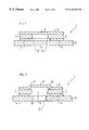
- FIG. 1 shows in a simplified partial representation and in cross section an initial copper-ceramic substrate
- FIG. 2 shows in the same representation as FIG. 1 the copper-ceramic substrate after its completion
- FIG. 3 shows the initial copper-ceramic substrate of FIG. 1 together with the tool for forming this substrate into the substrate of FIG. 2,
- FIGS. 4 and 5 show in a simplified partial representation and in cross section another initial copper-ceramic substrate immediately before its final completion or after its final completion, and together with the forming tool,
- FIGS. 6 and 7 show another possible version in a representation similar to FIGS. 4 and 5 .
- Initial copper-ceramic substrate 1 shown in FIG. 1 consists essentially of ceramic layer 2 which is provided on both surface sides each with a metallic coating in the form of copper layer 3 or 4 which is a metal foil or metal board.
- ceramic layer 2 as well as copper layer 4 which is the bottom one in FIGS. 1-3 are interrupted. This interruption 5 is produced, for example, by removing both the material of copper layer 4 and the material of ceramic layer 2 in the area of the interruption or opening 5 after applying copper layers 3 and 4 to ceramic layer 2 .
- DB process direct bonding process
- DCB process direct copper bonding process
- structured copper layer 3 which forms printed conductors and contact surfaces bridges opening 5 with sub-area 3 ′.
- the side of bottom copper layer 4 facing away from copper layer 3 is joined to copper plate 6 (support plate) which has a thickness which is much greater compared to copper layers 3 and 4 and via which substrate 1 or the power circuit formed by this substrate and electrical components which are not shown are attached to a heat sink for dissipating heat loss which is not shown.
- opening 5 in the area of copper layer 4 has a greater width than in the area of ceramic layer 2 so that viewed from copper layer 3 the border of copper layer 4 in the area of recess 5 lies hidden behind the border of ceramic layer 2 , the border directly delimiting opening 5 and thus the distance decisive for electrical insulation between copper layers 3 and 4 is enlarged.
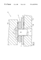
- substrate 1 To transform substrate 1 into substrate 1 ′ which, compared to substrate 1 , has a much higher dielectric strength and reduced susceptibility to cracking during temperature cycles, through hole 8 is made first in copper plate 6 which, for example is joined by brazing to copper plate 4 in the area of opening 5 . Subsequently substrate 1 is inserted into tool 9 which has two plate-shaped tool parts 10 and 11 . Between the latter, substrate 1 is clamped flat so that it rests flat with its upper copper layer 3 against one surface of female die-like tool part 10 and flat against one surface of tool part 11 with copper plate 6 . Tool part 10 on this bearing surface where arched bridge 3 ′′ is to be produced has a concave recess 12 .
- Recess 12 has a width which is greater than the corresponding width of opening 5 in ceramic layer 2 so that when sub-area 3 ′ is deformed into bridge 3 ′′ at the same time, the copper of copper layer 3 is detached at the same time also from the top of ceramic layer 2 on border areas 7 in each case. The width of these areas or the detachment can be determined very exactly by the width of recess 12 .
- FIGS. 4 and 5 show substrate 1 a or 1 a ′, in which substrate 1 a ′ is produced by mechanical forming from substrate 1 a and has higher dielectric strength and reduced tendency to cracking.
- substrate 1 a which is shown like substrate 1 a ′ in the area of one border consists of ceramic layer 2 and upper and lower copper layer 3 and 4 .
- the upper copper layer which in turn is structured to form printed conductors, contact surfaces, etc. forms on border 14 of the substrate a projecting flap or projection 15 which is, for example, an external connection of the electrical circuit.
- the latter is set back with its border opposite the border of ceramic layer 2 so that for substrate 1 a a distance decisive for dielectric strength results between copper layers 3 and 4 which is somewhat greater than the thickness of ceramic layer 2 and moreover a reduced tendency to thermomechanically induced cracking is obtained. At higher voltages this distance however is not adequate.
- substrate 1 a is formed into substrate 1 a ′ in which instead of projection 15 , projection 15 ′ is formed and copper layer 3 in the area of border 14 is deformed in an S-shape such that projection 15 ′ has a greater distance from the plane of copper layer 4 not only in the direction of the vertical substrate plane, but on border 14 copper layer 3 is also detached in one edge area 16 from ceramic layer 2 , in this way therefore the distance decisive for dielectric strength between copper layers 3 and 4 along ceramic layer 2 is significantly increased.
- Forming tool 17 which has a total of four tool parts 18 and 19 or 20 and 21 which are each provided in pairs and which are shaped like clamps is used to shape substrate 1 a into substrate 1 a ′ with higher dielectric strength and reduced tendency to thermomechanically induced cracking.
- substrate 1 a is clamped between tool parts 18 and 19 , tool part 18 lying flat against copper layer 3 and tool part 19 lying flat against copper layer 4 and at least tool part 18 with its border 18 ′ which runs parallel to border 14 having a certain distance from border 14 of substrate 1 a or ceramic layer 2 . This distance then determines the width of detached area.
- FIGS. 6 and 7 show substrate 1 b and substrate 1 b ′ obtained therefrom by shaping.
- Substrate 1 b consists of ceramic layer 2 which is continuously slotted at 22 or is provided with a predetermined breaking point, for example, by laser cutting, by mechanical scratching or similar techniques.
- ceramic layer 2 are upper and lower copper layer 3 or 4 in turn, lower copper layer 4 being interrupted in the area of the slot or predetermined breaking point 22 .
- substrate 1 b is shaped into substrate 1 b ′ (FIG. 7 ). For this reason the substrate is clamped flat between tool parts 20 and 21 with its part formed in FIGS. 6 and 7 to the right of predetermined breaking point 22 between tool parts 18 and 19 and with its part to the left of predetermined breaking point 22 .
- the two tool parts 20 and 21 are then swivelled relative to tool parts 18 and 19 , according to arrow B of FIG.
- substrate lb forms two sections bent relative to one another and each are formed by one side of bent copper layer 3 which holds these sections together, part of ceramic layer 2 and part of copper layer 4 .
- the side of copper layer 3 facing away from ceramic layer 2 is turned to the angular space formed by the bend.
Abstract
Description
| List of |
| 1, 1′ | Substrate | ||
| 1a, 1a′ | |
||
| 1b, 1b′ | |
||
| 2 | |
||
| 3 | |
||
| 3′ | |
||
| 3″ | |
||
| 4 | |
||
| 5 | |
||
| 5′ | |
||
| 6 | |
||
| 7 | Area | ||
| 8 | Hole | ||
| 9 | |
||
| 10, 11 | |
||
| 12 | Recess | ||
| 13 | Male die | ||
| 14 | |
||
| 15, 15′ | |
||
| 16 | |
||
| 17 | Tool | ||
| 18-21 | |
||
| 18′, 20′ | |
||
| 22 | |
||
| 23 | |
||
| 24 | Area | ||
Claims (16)
Priority Applications (1)
| Application Number | Priority Date | Filing Date | Title |
|---|---|---|---|
| US08/665,967 US6182358B1 (en) | 1993-06-03 | 1996-06-21 | Process for producing a metal-ceramic substrate |
Applications Claiming Priority (4)
| Application Number | Priority Date | Filing Date | Title |
|---|---|---|---|
| DE4318463 | 1993-06-03 | ||
| DE4318463A DE4318463C3 (en) | 1993-06-03 | 1993-06-03 | Method of manufacturing a metal-ceramic substrate |
| US25324594A | 1994-06-02 | 1994-06-02 | |
| US08/665,967 US6182358B1 (en) | 1993-06-03 | 1996-06-21 | Process for producing a metal-ceramic substrate |
Related Parent Applications (1)
| Application Number | Title | Priority Date | Filing Date |
|---|---|---|---|
| US25324594A Continuation | 1993-06-03 | 1994-06-02 |
Publications (1)
| Publication Number | Publication Date |
|---|---|
| US6182358B1 true US6182358B1 (en) | 2001-02-06 |
Family
ID=6489556
Family Applications (1)
| Application Number | Title | Priority Date | Filing Date |
|---|---|---|---|
| US08/665,967 Expired - Lifetime US6182358B1 (en) | 1993-06-03 | 1996-06-21 | Process for producing a metal-ceramic substrate |
Country Status (3)
| Country | Link |
|---|---|
| US (1) | US6182358B1 (en) |
| EP (1) | EP0632684B1 (en) |
| DE (2) | DE4318463C3 (en) |
Cited By (4)
| Publication number | Priority date | Publication date | Assignee | Title |
|---|---|---|---|---|
| US20030110627A1 (en) * | 2000-05-30 | 2003-06-19 | Gottfried Ferber | Substrate for receiving a circuit configuration and method for producing the substrate |
| US6858151B2 (en) * | 2002-06-14 | 2005-02-22 | Dowa Mining Co., Ltd. | Metal/ceramic bonding article and method for producing same |
| WO2013167123A1 (en) * | 2012-05-10 | 2013-11-14 | Curamik Electronics Gmbh | Method for producing metal-ceramic substrates, and metal-ceramic substrate produced according to said method |
| CN113853365A (en) * | 2019-05-20 | 2021-12-28 | 罗杰斯德国有限公司 | Method for producing a metal-ceramic substrate and metal-ceramic substrate produced by said method |
Families Citing this family (8)
| Publication number | Priority date | Publication date | Assignee | Title |
|---|---|---|---|---|
| DE19527611B4 (en) * | 1995-07-28 | 2006-05-24 | Schulz-Harder, Jürgen, Dr.-Ing. | Method for producing a substrate for electrical circuits |
| DE19609929B4 (en) * | 1996-03-14 | 2006-10-26 | Ixys Semiconductor Gmbh | The power semiconductor module |
| DE19614501C2 (en) * | 1996-04-13 | 2000-11-16 | Curamik Electronics Gmbh | Process for producing a ceramic-metal substrate and ceramic-metal substrate |
| DE19748005A1 (en) * | 1997-10-30 | 1999-05-20 | Siemens Ag | Arrangement for transmitting electrical signals between a module that is thermally insulated on a carrier plate and adjacent neighboring modules |
| DE19914815A1 (en) * | 1999-03-31 | 2000-10-05 | Abb Research Ltd | Semiconductor module |
| DE102009044933B4 (en) * | 2009-09-24 | 2023-03-30 | Infineon Technologies Ag | Power semiconductor module with at least two connected circuit carriers and method for producing a power semiconductor module with at least two connected circuit carriers |
| DE102012102787B4 (en) * | 2012-03-30 | 2015-04-16 | Rogers Germany Gmbh | Method for producing metal-ceramic substrates |
| DE102016119485A1 (en) | 2016-10-12 | 2018-04-12 | Infineon Technologies Ag | A chip carrier having an electrically conductive layer that extends beyond a thermally conductive dielectric sheet structure |
Citations (9)
| Publication number | Priority date | Publication date | Assignee | Title |
|---|---|---|---|---|
| US3487541A (en) * | 1966-06-23 | 1970-01-06 | Int Standard Electric Corp | Printed circuits |
| US4295184A (en) * | 1978-08-21 | 1981-10-13 | Advanced Circuit Technology | Circuit board with self-locking terminals |
| US4500029A (en) * | 1982-06-11 | 1985-02-19 | General Electric Company | Electrical assembly including a conductor pattern bonded to a non-metallic substrate and method of fabricating such assembly |
| US4527330A (en) * | 1983-08-08 | 1985-07-09 | Motorola, Inc. | Method for coupling an electronic device into an electrical circuit |
| US4737236A (en) * | 1986-09-08 | 1988-04-12 | M/A-Com, Inc. | Method of making microwave integrated circuits |
| US4831723A (en) * | 1988-04-12 | 1989-05-23 | Kaufman Lance R | Direct bond circuit assembly with crimped lead frame |
| DE3931551A1 (en) | 1989-09-22 | 1991-04-04 | Schulz Harder Juergen | Copper and ceramic multilayer substrate prodn. - involving slitting of ceramic layers to avoid thermal stress damage |
| US5029386A (en) * | 1990-09-17 | 1991-07-09 | Hewlett-Packard Company | Hierarchical tape automated bonding method |
| US5353499A (en) * | 1992-04-20 | 1994-10-11 | Sumitomo Electric Industries, Ltd. | Method of manufacturing a multilayered wiring board |
Family Cites Families (4)
| Publication number | Priority date | Publication date | Assignee | Title |
|---|---|---|---|---|
| US3911553A (en) * | 1974-03-04 | 1975-10-14 | Gen Electric | Method for bonding metal to ceramic |
| DE3941814A1 (en) * | 1988-11-05 | 1991-06-20 | Semikron Elektronik Gmbh | Carrier plate for power semiconductor components - has metal plate provided with ceramics disc divided into pieces between metallised areas |
| DE4004844C1 (en) * | 1990-02-16 | 1991-01-03 | Abb Ixys Semiconductor Gmbh | Copper metallisation on ceramic substrate - obtd. by bonding copper foil directly to whole surface of substrate, then masking and etching |
| US5328751A (en) * | 1991-07-12 | 1994-07-12 | Kabushiki Kaisha Toshiba | Ceramic circuit board with a curved lead terminal |
-
1993
- 1993-06-03 DE DE4318463A patent/DE4318463C3/en not_active Expired - Lifetime
-
1994
- 1994-05-21 EP EP94107879A patent/EP0632684B1/en not_active Expired - Lifetime
- 1994-05-21 DE DE59409429T patent/DE59409429D1/en not_active Expired - Lifetime
-
1996
- 1996-06-21 US US08/665,967 patent/US6182358B1/en not_active Expired - Lifetime
Patent Citations (9)
| Publication number | Priority date | Publication date | Assignee | Title |
|---|---|---|---|---|
| US3487541A (en) * | 1966-06-23 | 1970-01-06 | Int Standard Electric Corp | Printed circuits |
| US4295184A (en) * | 1978-08-21 | 1981-10-13 | Advanced Circuit Technology | Circuit board with self-locking terminals |
| US4500029A (en) * | 1982-06-11 | 1985-02-19 | General Electric Company | Electrical assembly including a conductor pattern bonded to a non-metallic substrate and method of fabricating such assembly |
| US4527330A (en) * | 1983-08-08 | 1985-07-09 | Motorola, Inc. | Method for coupling an electronic device into an electrical circuit |
| US4737236A (en) * | 1986-09-08 | 1988-04-12 | M/A-Com, Inc. | Method of making microwave integrated circuits |
| US4831723A (en) * | 1988-04-12 | 1989-05-23 | Kaufman Lance R | Direct bond circuit assembly with crimped lead frame |
| DE3931551A1 (en) | 1989-09-22 | 1991-04-04 | Schulz Harder Juergen | Copper and ceramic multilayer substrate prodn. - involving slitting of ceramic layers to avoid thermal stress damage |
| US5029386A (en) * | 1990-09-17 | 1991-07-09 | Hewlett-Packard Company | Hierarchical tape automated bonding method |
| US5353499A (en) * | 1992-04-20 | 1994-10-11 | Sumitomo Electric Industries, Ltd. | Method of manufacturing a multilayered wiring board |
Cited By (6)
| Publication number | Priority date | Publication date | Assignee | Title |
|---|---|---|---|---|
| US20030110627A1 (en) * | 2000-05-30 | 2003-06-19 | Gottfried Ferber | Substrate for receiving a circuit configuration and method for producing the substrate |
| US6858807B2 (en) * | 2000-05-30 | 2005-02-22 | Eupec Europaeische Gesellschaft Fuer Leistungshalbleiter Mbh | Substrate for receiving a circuit configuration and method for producing the substrate |
| US6858151B2 (en) * | 2002-06-14 | 2005-02-22 | Dowa Mining Co., Ltd. | Metal/ceramic bonding article and method for producing same |
| WO2013167123A1 (en) * | 2012-05-10 | 2013-11-14 | Curamik Electronics Gmbh | Method for producing metal-ceramic substrates, and metal-ceramic substrate produced according to said method |
| DE102012104903B4 (en) | 2012-05-10 | 2023-07-13 | Rogers Germany Gmbh | Process for producing metal-ceramic substrates and metal-ceramic substrate produced by this process |
| CN113853365A (en) * | 2019-05-20 | 2021-12-28 | 罗杰斯德国有限公司 | Method for producing a metal-ceramic substrate and metal-ceramic substrate produced by said method |
Also Published As
| Publication number | Publication date |
|---|---|
| EP0632684A3 (en) | 1995-11-08 |
| EP0632684A2 (en) | 1995-01-04 |
| DE4318463C3 (en) | 2001-06-21 |
| DE4318463A1 (en) | 1994-12-08 |
| EP0632684B1 (en) | 2000-07-12 |
| DE59409429D1 (en) | 2000-08-17 |
| DE4318463C2 (en) | 1995-07-27 |
Similar Documents
| Publication | Publication Date | Title |
|---|---|---|
| US5661086A (en) | Process for manufacturing a plurality of strip lead frame semiconductor devices | |
| US6182358B1 (en) | Process for producing a metal-ceramic substrate | |
| EP1453089B1 (en) | Semiconductor substrates of high reliability | |
| US5938104A (en) | Direct metal bonding | |
| US5465898A (en) | Process for producing a metal-ceramic substrate | |
| JPH0777246B2 (en) | Ceramics circuit board | |
| US6207221B1 (en) | Process for producing a metal-ceramic substrate and a metal-ceramic substrate | |
| EP1791176B1 (en) | Method of manufacturing a power module substrate | |
| US4500029A (en) | Electrical assembly including a conductor pattern bonded to a non-metallic substrate and method of fabricating such assembly | |
| KR100374379B1 (en) | Substrate | |
| US5924191A (en) | Process for producing a ceramic-metal substrate | |
| JP4765110B2 (en) | Metal-ceramic bonding substrate and manufacturing method thereof | |
| JPS615596A (en) | Method of producing circuit board and circuit pattern frame used therefor | |
| CN111787710A (en) | Preparation method of ceramic circuit board | |
| JPH04103150A (en) | Ic mounting board | |
| JP2640780B2 (en) | Interlayer connection method for metal substrates | |
| US3581386A (en) | Methods of manufacturing semiconductor devices | |
| JPH06177513A (en) | Manufacture of circuit substrate | |
| JP3000083B2 (en) | Manufacturing method of electronic parts container | |
| JP2004080063A (en) | High-reliability substrate for semiconductor | |
| US20050095748A1 (en) | Method for the selective surface treatment of planar workpieces | |
| EP0851723A1 (en) | Method for mounting electronic parts | |
| JP5052290B2 (en) | Manufacturing method of circuit board with metal fittings | |
| JPH0519315B2 (en) | ||
| JPH02137391A (en) | Manufacture of printed wiring board with metal-sheet base |
Legal Events
| Date | Code | Title | Description |
|---|---|---|---|
| STCF | Information on status: patent grant |
Free format text: PATENTED CASE |
|
| FPAY | Fee payment |
Year of fee payment: 4 |
|
| AS | Assignment |
Owner name: ELECTROVA AG, AUSTRIA Free format text: ASSIGNMENT OF ASSIGNORS INTEREST;ASSIGNOR:SCHULZ-HARDER, JURGEN;REEL/FRAME:017125/0926 Effective date: 20051118 |
|
| FEPP | Fee payment procedure |
Free format text: PAT HOLDER NO LONGER CLAIMS SMALL ENTITY STATUS, ENTITY STATUS SET TO UNDISCOUNTED (ORIGINAL EVENT CODE: STOL); ENTITY STATUS OF PATENT OWNER: LARGE ENTITY |
|
| REFU | Refund |
Free format text: REFUND - PAYMENT OF MAINTENANCE FEE, 8TH YR, SMALL ENTITY (ORIGINAL EVENT CODE: R2552); ENTITY STATUS OF PATENT OWNER: LARGE ENTITY |
|
| FPAY | Fee payment |
Year of fee payment: 8 |
|
| FEPP | Fee payment procedure |
Free format text: PAYOR NUMBER ASSIGNED (ORIGINAL EVENT CODE: ASPN); ENTITY STATUS OF PATENT OWNER: LARGE ENTITY |
|
| AS | Assignment |
Owner name: CURAMIK HOLDING GMBH, IN LIQUIDATION, GERMANY Free format text: CHANGE OF NAME;ASSIGNOR:ELECTROVAC AG;REEL/FRAME:026015/0157 Effective date: 20110218 Owner name: CURAMIK ELECTRONICS GMBH, GERMANY Free format text: ASSIGNMENT OF ASSIGNORS INTEREST;ASSIGNOR:CURAMIK HOLDING GMBH IN LIQUIDATION;REEL/FRAME:026015/0375 Effective date: 20110131 |
|
| FEPP | Fee payment procedure |
Free format text: PAYER NUMBER DE-ASSIGNED (ORIGINAL EVENT CODE: RMPN); ENTITY STATUS OF PATENT OWNER: LARGE ENTITY Free format text: PAYOR NUMBER ASSIGNED (ORIGINAL EVENT CODE: ASPN); ENTITY STATUS OF PATENT OWNER: LARGE ENTITY |
|
| FPAY | Fee payment |
Year of fee payment: 12 |
|
| AS | Assignment |
Owner name: ROGERS GERMANY GMBH, GERMANY Free format text: CHANGE OF NAME;ASSIGNOR:CURAMIK ELECTRONICS GMBH;REEL/FRAME:033347/0420 Effective date: 20140507 |